MOOSE: A Physically Based Compact DC Model of
SOI LDMOSFETs for Analogue Circuit Simulation
Nele V. T. D’Halleweyn, James Benson, William Redman-White
, Member, IEEE
, Ketan Mistry, and
Maarten Swanenberg
Abstract—In this paper, we present a compact model for sil-icon-on-insulator (SOI) laterally double diffused (LD) MOSFETs. The model is complete insofar as it uses no subcircuits, and is intended to predict device operation in all regions of bias. The device current is described by two main equations handling the MOS channel and the drift region, both of which are smooth and continuous in all operating regimes. Attention is also given to the modeling of inversion at the back oxide to ensure correct behavior is predicted for a source follower in power control applications (“high side operation”). A surface-potential-based formulation is used for the inversion/accumulation channel giving smooth transitions between different regions of operation, and care has been taken to ensure all expressions are smooth and infinitely differentiable to achieve the best possible convergence perfor-mance. Self (and coupled) heating effects exert a major influence over the behavior of power SOI devices, and these issues are incorporated in the model core in a consistent fashion.The model has been installed in a commercial SPICE-type circuit simulator and evaluated against individual devices and complete circuits fabricated in an industrial smart power SOI process. Accuracy is significantly improved with respect to the existing LDMOS models, and convergence behavior in switching and linear circuit simulations is comparable with industry standard models of this complexity.
Index Terms—Analogue circuits, compact models, laterally double diffused (LD) MOSFET, MOS devices, silicon-on-insulator technology, simulation.
I. INTRODUCTION
A
S THE scaling down of smart power ICs is gaining in importance, silicon-on-insulator (SOI) technology is be-coming more attractive. Compared with a bulk technology, SOI offers a far better isolation scheme [1] leading to improved cir-cuit density, and exhibits a significantly lower on-resistance for source-high conditions [2].Manuscript received November 20, 2002; revised December 12, 2003. This paper was recommended by Associate Editor S. Saxena.
N. V. T. D’Halleweyn was with the Microelectronics Centre, Department of Electronics and Computer Science, University of Southampton SO17 1BJ, UK. She is now with Arnold en Siedsma, 2018 Antwerp, Belgium.
J. Benson was with the Microelectronics Centre, Department of Electronics and Computer Science, University of Southampton SO17 1BJ, United Kingdom. He is now with the Advanced Technology Institute, University of Surrey, Guild-ford GU2 7XH, UK (e-mail: [email protected]).
W. Redman-White is with the Microelectronics Centre, Department of Elec-tronics and Computer Science, University of Southampton SO17 1BJ, UK.
K. Mistry was with the Microelectronics Centre, Department of Electronics and Computer Science, University of Southampton SO17 1BJ, UK. He is now with the Department of Electronic and Electrical Engineering, University Col-lege Dublin, Dublin, Ireland.
M. Swanenberg is with Philips Semiconductors, 6534 AE Nijmegen, The Netherlands.
Digital Object Identifier 10.1109/TCAD.2004.835125
The LDMOS transistor is one of the key devices in high voltage (HV) ICs, and a good model is indispensable in order to perform accurate circuit design. Some subcircuit models for bulk and SOI LDMOS devices are available, but, when certain specific aspects of device behavior become critical, they are not always sufficient. Moreover, they also suffer from a higher degree of complexity, compared with a compact model and, hence, an increase in computation time and a more complex parameter extraction procedure. The need for an accurate, robust compact model is therefore apparent.
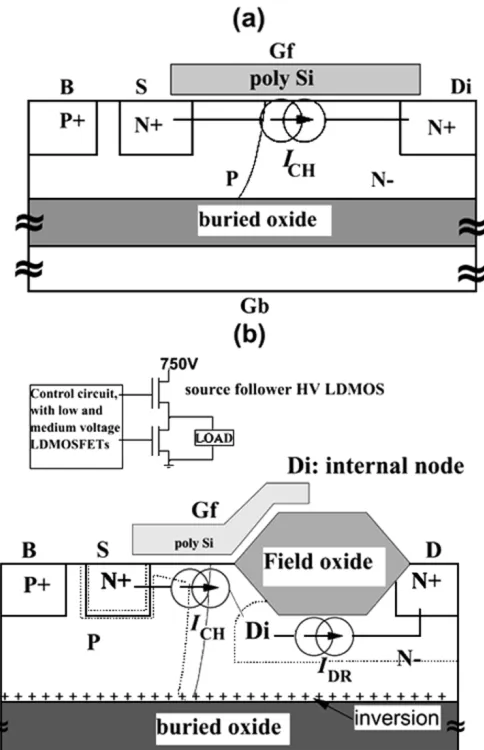
In the general class of SOI LDMOS devices with a constant doping profile in the drift region, two different structures can be distinguished, each designed for a different range of drain voltages. The first type does not contain a field oxide, and the thin gate oxide extends over the drift region all the way to the drain. This device is illustrated in Fig. 1(a) and will be referred to as the low voltage (LV) SOI LDMOS. In the second type, a thicker oxide (field oxide) is grown on the drift region to bend back the equipotential lines and reduce the fringing fields at the edge of the polysilicon gate. This construction is shown in Fig. 1(b) and will be referred to as the medium voltage (MV) LDMOS. Note that the model can also be used for the offset drain structure, being the MV structure with the thickness of the field oxide being zero. HV LDMOS transistors often have a graded doping profile in the drift region to fullfill the conditions of the RESURF principle [3], [4], or use superjunction tech-niques [5]. At present, these HV devices are very technology de-pendent, and it would be difficult to develop one general model for this type of device; this task is left for a succeeding research project.
Compact models for SOI LDMOS transistors have received much attention in the literature [6]–[10]. The main difference between SOI and bulk structures is to be found in the drift re-gion; for SOI, the lightly doped drift region rests on a thick oxide, while, in a bulk device, it sits on top of a -type sub-strate. The modeling of the MOS channel part with the doping gradient in the inversion channel is similar for both technolo-gies. The vertical and lateral bulk DMOS models from the Uni-versity of Florida [6]–[9] take this lateral doping gradient in the channel into account, albeit only partly. In the Motorola LDMOS model [10] this gradient can be accounted for by par-titioning the channel into regions of constant doping, and thus creating more internal nodes; this is accurate, but increases the computation time considerably.
Our model aims to describe in particular LV and MV SOI LDMOS transistors, which have a constant doping concentra-tion in the drift region. Particular emphasis has been placed on
Fig. 1. Definition of the dc currents: (a) LV LDMOS and (b) MV LDMOS working under high side conditions.
the behavior and circuit-level modeling issues related to high-side drive applications, and on the self- and mutual heating. For the -type LDMOS, high-side operation increases the on-resis-tance and demands specific modeling effort. To describe accu-rately the behavior of the MV SOI LDMOS, we use two cur-rent equations, both of which are smooth and continuous in all regions of operation. These two current expressions have been matched consistently with the help of limiting procedures and an accurate prediction of the internal node voltage. MOOSE can be made to converge more quickly than a compound subcircuit model, since the internal node voltage is set automatically to some reasonable initial estimate, calculated within the model.
Although it is not intended to be the main focus of this paper, a comparison between the two types of models was made by con-structing subcircuit models and comparing their performance with the MOOSE compact model when running single device and test circuit simulations [11]. That subcircuit models are sub-ject to a higher risk of convergence failure was indeed con-firmed. Furthermore, the subcircuit models were found to be somewhat limited in the types of physical effects that could be modeled. For instance, accurate modeling of self-heating effects was not possible, unless a separate thermal node was added to
each device model. Charge modeling was also problematic. Ad-ditionally, more parameters were required, and these tended to be less physical than in a compact model, and more difficult to extract. Despite these drawbacks, the subcircuit models still managed to provide good agreement with DC measurements, and reasonable matching for transient and AC results. The issue of poor convergence speed could not however be resolved using these models; we now turn our attention to the development of our compact model.
In Section II, we develop the first current expression , which describes the LV LDMOS part, including the drift region under the thin gate oxide. The formulation for the current under the thin gate oxide is surface potential based, and models both the drift and diffusion currents in all operating regions. Care has been taken to use only continuous and infinitely differen-tiable expressions. Furthermore, the model ensures a smooth transition between subthreshold and strong inversion and be-tween triode and saturation. Both the lateral doping gradient in the channel and the overlap of the thin gate oxide over the drift region are accounted for in a compact and physical manner.
In Section III, we explain the second expression , which models the drift region under the field oxide and includes high-side behavior. By using both the potential in the drift region and the surface potential at the surface of the buried oxide, we ensure a purely physical prediction of the unique high-side behavior observed in the SOI LDMOS. Fig. 1 illustrates where and are applicable in the LV and MV SOI LDMOS structures. The MOOSE model combines an electrical model with a thermal network to model self- and coupled heating effects in a consistent manner. In Section IV, the implementation of the internal thermal netlist is discussed.
The model has been implemented in the SPICE circuit sim-ulator and careful formulation and coding has led to a very ro-bust SOI LDMOS model, which converges easily without the frequent need for node setting commands. The model has been thoroughly evaluated, both qualitatively, using a set of simula-tions based on the SEMATECH tests [12], and quantitatively, verifying single device characteristics against measurements for different geometries. Some key results are presented in Sec-tion V.
II. CURRENTUNDERTHIN-GATEOXIDE
To derive , we define first the surface potentials with re-spect to the -body (B), in all regions of operation. The different symbols used in this section are defined in Fig. 2. We consider three regimes, these being strong inversion, subthreshold, and saturation. Using a logarithmic smoothing function to join the various components, we arrive at the following expression [13]:
(1)
(2)
Fig. 2. Symbols used for the calculation ofI .
where is a smoothing parameter equal to the thermal voltage, . The expression for is developed in Sec-tion II-D. It is shown that in the subthreshold region and in the saturation regime. For more details about the physical background, refer to [14].
A. Inversion-Channel Current
Using standard assumptions for MOSFETs [14], the inver-sion-channel current can be expressed using the classic charge-sheet model [15]. Using the electron continuity equation [16] and neglecting recombination and generation currents yields
(4)
where is the channel charge density, the surface po-tential at position the surface mobility, and the ef-fective length of the channel, defined by the length of the un-derdiffusion of the -well minus the underdiffusion of the
source well . is denoted by at
and by at .
The mobility is initially assumed to be constant along the channel. Using the depletion approximation, which assumes that the depletion region under the gate is free of mobile carriers [17], the inversion channel charge can be obtained as
(5)
with the thin-gate oxide
capaci-tance per unit area, and the body factor is given by .
In order to get an analytic closed-form expression for the saturation voltage when including high field effects (see Sec-tion II-D), the body charge is linearized using a Taylor expan-sion for the square root term [18]
(6) (7)
with .
The LDMOS has a nonuniformly doped channel region, starting at the end of the source diffusion and ending where
the -implant equals the -type background doping. Thus, the doping concentration along the channel has a maximum near the source and decreases sharply toward the drain . The lateral doping gradient in the channel is brought in by means of , which is a function of and thus of the position along the channel. In order to perform the integration of (4), is needed in terms of only, or in other words, we have to transform to . This can only be done under certain assumptions, which are set out below.
The doping profile is assumed to be exponential [9], [8] and hence
(8)
with . To transform into
is assumed to be a linear function of , i.e.,
(9)
This yields
(10)
In a standard MOSFET with a constant doping in the channel, the linearity of with is accurate for low drain biases, but deteriorates toward higher drain biases. However, a decreasing doping concentration in the channel causes areduced field effect, giving a reasonable linearity for higher drain biases. This has been confirmed using ATLAS simulations [11]. Furthermore, the MOS part of the LDMOS never reaches very deep saturation because the main part of the applied voltage drops over the drift region.
Using (10) and (7), the inversion channel density can be ex-pressed as a function of only. Substituting this expression into (4) results in a closed-form continuous equation, which can be used for the inversion-channel current in all regions of oper-ation
(11)
with
(12)
(13)
(14)
(15)
(16)
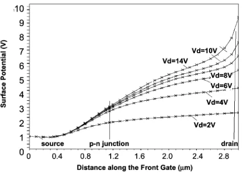
Fig. 3. ATLAS simulation of the depletion layers and the surface potential under the front gate (V = 4V).
B. Accumulation/Drift Current Under Thin Gate Oxide In linear region operation, an accumulation layer exists in the drift region under the thin oxide, and this has a significant impact on device behavior. In bulk and SOI compact models published so far [7], [9], [19] this effect is neglected, or else an additional current source is added [10], slowing down convergence. In this work, we handle the issue analytically without introducing an extra node.
Since the length of this part of the drift region is typ-ically comparable with the channel length, we assume that the channel current saturates before the accumulation layer starts to disappear at the drain, and ATLAS [20] simulations confirm the validity of this approach (Fig. 3). Further, when looking at the measured output characteristics of an LV LDMOS (see Fig. 8), it can be observed that the current saturates before reaches
.
Neglecting the diffusion current and assuming that the surface is completely accumulated, the current in the drift region under the front gate can be expressed by [21]
(17)
where is the low field mobility in the drift region, is the surface mobility in the accumulation region, and is the free bulk charge density in the region, and the surface accumulation charge density:
(18) (19)
where is the doping concentration in the drift region and is a fitting parameter taking into account the fact that the cur-rent flow is partially vertical. This is due to the curcur-rent flow lines being longer than , especially when is of the same order as the silicon film thickness . When is consider-ably larger than this factor should approach one.
To ensure zero model current when , we use instead of . The difference between
and is usually negligible ( V), be-cause, considered on a logarithmic scale, the doping concentra-tions of the -body and the drift region are comparable.
After integration of (17) we obtain
(20)
with
(21)
(22)
(23)
(24)
This expression completely describes the drift current under the thin gate oxide with a second order equation in the surface po-tentials and . Note that can be recognized as the ON-resistance of the drift region under the thin gate oxide under zero bias conditions, and is the accumulation layer gain factor.
C. Solving for Surface Potential at the End of the Inversion Channel
Having obtained expression for the inversion-layer channel current and the drift current under the thin-gate oxide , an analytical expression for the surface potential at the - junction can be derived. To find when the channel is in strong inversion , (11) is equated to (20), and yields as a function of the known surface potentials and
(25)
with
(26) (27)
(28)
(29)
(30)
D. Inclusion of High Field Effects
1) Vertical Field Mobility Reduction: Using the linearized expression for the body and the channel charge densities [(7) and (5)], the transverse electric field becomes [22]
where is an empirical parameter, taking on the value for electrons and for holes, and a mean value for the body factor has been defined as .
Averaging over the length of the device and using this av-erage in the expression for the effective mobility for an -type device (assuming classical diffuse scattering at the Si-SiO sur-face) yields
(32)
with the vertical field mobility coefficient. Note that it is im-portant to include the linearized root terms in HV devices be-cause the doping concentration of the -body is often higher than for standard CMOS, leading to a higher body factor and hence an increased importance of these terms.
2) Carrier-Velocity Saturation: When the longitudinal field increases, the carrier velocity increases proportionally to the field strength, until eventually reaching the saturation velocity
. The critical field for which this happens is given by . This effect is modeled as [14]
(33)
3) Combined Mobility Model: The two high-field effects give rise to (34), which is shown at the bottom of the page for the high-field effective mobility.
In [6], it is claimed that velocity saturation in LDMOS tran-sistors occurs at the source side because the doping concentra-tion is highest there, but this is not proven. The posiconcentra-tion of the lateral field maximum also depends on the applied biases and, on whether velocity saturation occurs before channel pinch-off, i.e., for very short channel length devices, the onset position will probably move along the channel. For long channel de-vices, pinch-off generally happens before velocity saturation, and velocity saturation takes place at the internal drain junc-tion, where the lateral field is highest. Considering the above arguments, characterizing saturation by electron velocity satu-ration at a fixed position [6] is questionable. To find the satura-tion-surface potential at , we search for the value of for which the channel current reaches a maximum and avoid the problem of the peak position of the lateral field
(35)
If we consider only the drift part of the channel current, which means neglecting in (14), we find
(36) with
(37)
(38)
(39)
Let us now have a closer look at the expression for
(40)
(41)
(42)
In the strong inversion case, the term can be neglected, compared with . On the other hand, in the subthreshold case, is zero, and neglecting the abovemen-tioned term means . So, under subthreshold conditions, we find , which is what we want. Rewriting (36) without that term gives the final expression for the satura-tion surface potential at
(43)
E. Calculation of the Saturation Voltage
In the previous section, the saturation surface potential at was calculated. To calculate the drain sat-uration voltage, , we look for for which
. This results in
(44)
with
(45)
and and as defined by (30) and (29).
To attain a smooth transition from triode into saturation re-gion a smoothing function is invoked to limit to [23]:
(46)
with an empirical parameter, which can take integer values only. For a short channel MOSFET, gives a good fit. For longer channel lengths, larger values of must be used.
F. Total Current Expression
All the different aspects of the current under the thin-gate oxide studied in the previous sections can now be joined to give the final formulation as seen in (47), located at the bottom of the page with and given by (1) and (2). The expression for is identical to (25), with the difference that is replaced by to include the saturation effects.
G. Auxiliary Model
The model also includes short and narrow channel effects, the channel-length modulation (CLM) effect, the DIBL effect, the parasitic bipolar effect, and impact ionization; these are all implemented in the same way as for standard SOI MOSFETs [14]. A couple of points need to be made however.
First, the CLM and DIBL effects in LDMOS transistors are much smaller than in a standard MOSFET because a large part of the drain voltage drops over the drift region. However, for low gate biases, it is important to take the CLM into account because it determines the value of the output conductance in the saturation regime.
Second, in LDMOS technology, it is common to place the body contact parallel with the source contact. This can lead to a relatively high body resistance, which is formed by the pinched region underneath the source junction. This body resistance, to-gether with the impact ionization back gate current, can switch on the lateral parasitic bipolar transistor (BJT), and this can de-termine the safe operating area of the LV and MV LDMOS [24]. The safe-operating area is reduced further by self-heating; when the device heats up, the effective body source voltage necessary to trigger the parasitic BJT becomes smaller. Furthermore, be-cause the BJT has a positive temperature dependent factor in the expression for the collector current, this effect can lead to early failure of the device.
III. DRIFTCURRENTUNDER THEFIELDOXIDE
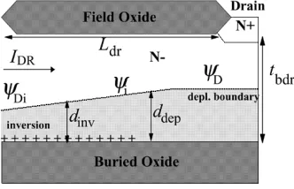
The current flow in the drift region is illustrated in Fig. 4. When the back gate voltage is negative, the surface at the buried oxide can be partially (as illustrated in Fig. 4) or fully inverted, depending on the channel potential .
A. Intrinsic Drift Current
Neglecting the diffusion contribution, the current can be written as in a depletion-type MOSFET with the back gate acting as the gate terminal [21]
(48)
[image:6.594.344.510.66.173.2]where is the depletion layer thickness extending from the buried oxide into the silicon, and the silicon thickness under the field oxide. Refer to Fig. 4 for the channel potentials and
Fig. 4. Current flow in the drift region under high side conditions.
. In this section, all potentials are defined with respect to the neutral bulk potential minus .
We consider two definitions for the depletion-layer thickness, before and after inversion. Before inversion this is given by [21]
(49)
with , and the buried oxide capacitance per unit area. In standard depletion-type MOSFET devices, the possibility of surface inversion is usually excluded for practical devices. However, when an LDMOS is working under high side conditions, the formation of an inversion layer is crucial to limit the further increase inON-resistance. If the surface at the buried oxide is inverted, the depletion layer thickness can be ex-pressed as
(50)
using the depletion-layer approximation from [17], and where the inversion surface potential is approximated as . To obtain closed-form analytical expressions for the saturation potentials in the next section, the square root of the surface po-tential is linearly approximated with a Taylor approximation around
(51)
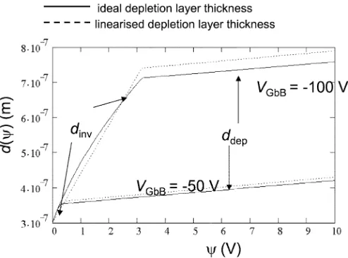
with . In Fig. 5, the linearized and ideal depletion layer thicknesses and are compared for typical parameters. Very good agreement is obtained for low values of and . For higher values, the deviation in-creases, but remains below 5%.
Using the linearized formulations for the integral in (48) can be rewritten as
(52)
Fig. 5. Comparison of the linearized (dotted line) and ideal (full line) formulation of the depletion layer thickness:d( )versus forV = 050 V and0100V.
where is the potential at the end of the inversion layer as de-noted in Fig. 4. This potential can be calculated from
(53)
with being the back gate-body
factor in the drift region. The potentials at the internal drain node and at the drain can be expressed in terms of the nodal voltages using and . Substituting (49), (51), and (53) into (52) results in
(54)
with
(55)
(56)
(57)
(58)
and . The “min” and “max”
functions describe a smooth and continuous minimum and max-imum respectively. Note that can be recognized as the
ON-resistance of the drift region under zero bias conditions. is the pinch-off voltage when the back surface is not in-verted and .
B. Saturation by Pinch-Off
The maximum value for the depletion layer thickness is . Assume here that ; otherwise and need only be swapped in the current equation. The pinch-off voltage can be found by equating to if (no inversion at the buried oxide), and to in the inverse case. It can be shown [11] that is given by the maximum of
(59)
(60)
To include saturation by pinch-off in the drift current expression, and have to be limited smoothly [11] to .
C. Velocity Saturation
For high drain biases the high field velocity saturation effects must be taken into account. Therefore, the low-field mobility
is replaced with [25]
(61)
with , where is the drift
satura-tion velocity.
To calculate the saturation potential, we solve
(62)
It can be proven [11] that the solution which is valid for all bias situations is shown in (63) at the bottom of the page with
(64)
where
(65)
(66)
with being a fitting parameter. Here, is limited to .
IV. MODELLINGHEATINGEFFECTS
Self-heating effects are a well-known complicating factor for high-power dissipation levels in DMOS [26]–[28] and other HV devices [29]. In a SOI technology, the thermal resistance is much higher than in its bulk counterpart, especially for HV devices where the buried oxide layer can be reasonably thick.
The finite thermal capacitance prevents the device tempera-ture from following the device power instantaneously, and so it is important to consider self-heating as a dynamic effect both in large and small signal terms [30]–[32]. The increase of the output conductance with frequency due to the thermal time con-stant (typically in the range of 100 kHz–1 MHz) is of extreme importance for analogue designers, since the output conduc-tance determines the gain of any amplifier.
In ultrathin RESURF SOI LDMOS structures, the distribu-tion of the heat generadistribu-tion in the drift region will be highly nonuniform, but will be reasonably constant in thicker SOI LDMOS devices [33], [34]. In compact models two-dimen-sional (2-D) heat-flow analysis [35] is too complicated, and it is usually preferred [14], [36] to assume thermal equilibrium and use an average temperature rise .
A separate circuit is used to model the thermal behavior of a device [37], [38], consisting of a thermal resistance and a thermal capacitance . Only one time constant has been em-bedded in the model, but if more are needed [39], a higher order network can be added externally. The thermal node can also be connected to a thermal interconnection network for the simula-tion of static and dynamic thermal coupling between devices.
In the case of a first order thermal circuit, the simulated tem-perature rise is obtained from
(67)
The dissipated power in the SOI LDMOS is given by
(68)
from which the simulated temperature rise can be deter-mined via (67). To find the small-signal equivalent, the thermal dissipation must be differentiated with respect to , and , just as with all the other electrical current expressions in the compact model. The temperature rise is treated as another voltage for which SPICE has to solve, and the local device temperature rise is available to circuit designers as a terminal voltage. Thermal dependence of model parameters is also included [14].
V. VALIDATION
Test chips were fabricated using a commercial HV SOI process containing single LV and MV LDMOS structures with different geometries. In this section, the measured data from the single devices are presented compared with MOOSE simu-lations. LV LDMOS devices with two different overlap lengths
( m and m, with m)
and MV LDMOS devices with three different drift lengths
( m, m, and m, with
[image:8.594.338.517.65.190.2]m) were selected for study and represent a com-prehensive range of geometries. Other relevant process details are: front gate oxide thickness nm, back gate oxide thickness m, silicon film thickness m, silicon thickness under field oxide m, and maximum doping concentration /cm .
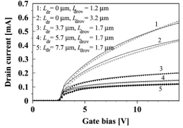
[image:8.594.336.516.242.365.2]Fig. 6. Measured (markers) and simulated (full line) drain current in the linear region for different geometries andV = 0:1V.
Fig. 7. Measured (markers) and simulated (full line) drain current in the linear regionV = 0; 01; 02V, andV = 0:1V.
The parameter extraction procedure used is very similar to the one used in compound models [40], although less parameters are required, which eases the optimization procedure.
A. Linear Characteristics
The linear characteristic for different geometries is shown in Fig. 6. As can be seen, the MOOSE model matches the measured data very well in almost all regions.
Curves 1 and 2 show the dracurrent decrease with in-creasing , and curves 3–5 show the current decrease with increasing . The match is very good for gate voltages more than 2 V above the threshold voltage but just above the threshold, the model slightly overestimates the measured current.
Fig. 8. LV LDMOS withL = 3:2 m; measured (markers) and simulated (full line) current vs.V forV = 3:5V,4:5V,5V,5:5V,8V,11V, and
[image:9.594.79.250.67.184.2]14V.
[image:9.594.81.245.240.356.2]Fig. 9. MV LDMOS withL = 1:7 m andL = 5:8 m; measured (markers) and simulated (full line) current versusV forV = 3:5V,4:5 V,5V,5:5V,8V,11V, and14V.
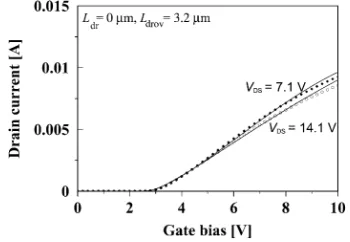
Fig. 10. LV LDMOS withL = 3:2 m; measured (markers) and simulated (full line) current versusV forV = 7:1V andV = 14:1V.
B. Output Characteristics
Output characteristics for the LV and MV LDMOS are shown in Figs. 8 and 9, respectively. In almost all cases, the model yields a good match with the measured data. The onset of sat-uration is well predicted, proving that pinch-off and satsat-uration effects in the drift region are well modeled. For the LV LDMOS, the drain-saturation current keeps increasing with the gate bias, while for the MV LDMOS the drift region limits the current much more noticeably. The model predicts well the decrease in current due to self-heating, which can lead to a negative output resistance in some bias situations.
This is also shown in Figs. 10 and 11. Self-heating is very noticeable in these curves because, above a certain gate voltage, the curves cross each other, leading to a higher current for the lower drain bias.
Fig. 11. MV LDMOS withL = 1:7 m andL = 5:8 m; measured (markers) and simulated (full line) current versusV forV = 7:1V and
V = 14:1V.
Fig. 12. Measured (markers) and simulated (full line) current forV = 10 V andV = 0V,050V,0100V, and0150V.
C. High-Side Behavior
Fig. 12 shows the device operated under high-side conditions. We observe a current decrease with increasingly negative back gate bias (i.e., substrate bias), but when inversion is established, the back gate voltage no longer influences the drain current. Good agreement is found between the simulated and measured data for curves 1–3. However, measured curve 4 has a positive slope, while the simulated curve 4 has saturated and has a nega-tive slope; this latter effect is due to self-heating and is masked prior to current saturation. One would expect the current for measured curve 4 to also have saturated due to pinch-off of the drift region, so that the current decreases with increasing . In reality, 2-D effects in the drift region may change the field distribution when is increased, or else enhanced CLM may occur with increasing back gate bias, thus delaying saturation and keeping the slope of the curve positive.
[image:9.594.333.518.253.382.2] [image:9.594.75.250.410.531.2]Fig. 13. MV LDMOS withL = 1:7 m andL = 5:8 m; measured (markers) and simulated (full line) current vs.V forV = 0:1V and
[image:10.594.287.548.63.227.2]V = 0V,050V,0100V.
Fig. 14. MV LDMOS withL = 1:7 m andL = 5:8 m; measured (markers) and simulated (full line) current versusV ; V = 10V;V =
2V, andV = 10V.
the drift region is reached , at which point the current stays constant.
D. Circuit Simulation Performance: Switching-Power Circuit
In this section, the influence of self-heating on some circuit blocks has been investigated and further insights about the com-pact model are set out. Obviously, the MOOSE model also in-cludes a full charge description [41], but to observe space re-strictions, we will concentrate on the dc aspects of the circuit.
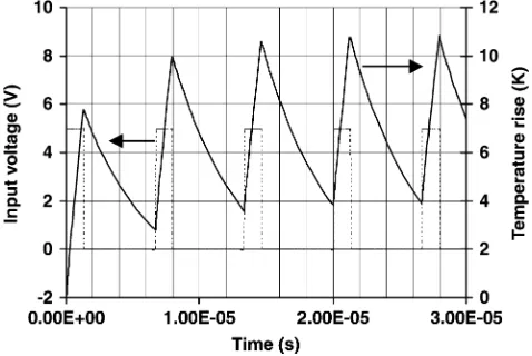
The circuit consists of a simplified horizontal line-driver cir-cuit for plasma displays as shown in Fig. 15. To investigate the self-heating behavior of the circuit, a load resistor was added between the output and the positive supply (see dotted lines in Fig. 15). The output voltage does not go all the way back to 0 V when Y12 is switched on, but reduces to a value determined by Y12 and the load resistor. The measured and simulated results for the MV circuit when are shown in Fig. 16. Due to self-heating the temperature of Y12 increases with time when it is on. This reduces the current in Y12 and results in a slight rise in the output voltage. In Fig. 17, the output voltage is plotted in detail and one can clearly observe the positive slope. In the same figure, the output voltage is simulated with and without self-heating; it is clear that including self-heating correctly pre-dicts the positive slope while the isothermal result shows a con-stant value for . Fig. 18 shows the simulated temperature
[image:10.594.311.537.276.439.2]Fig. 15. Circuit schematic for a switching power block.
Fig. 16. Simulated (full line) and measured (markers) output voltage of a plasma display driver switching circuit with a resistive load(R = 73 )to the positive supply voltage (LV circuit).
Fig. 17. Detail of the measured (markers) and simulated (with (full line) and without (dotted line) self-heating) positive slope from the switching circuit in Fig. 15.
[image:10.594.73.260.287.411.2] [image:10.594.312.543.509.672.2]Fig. 18. Simulated temperature rise of the output transistor Y12 in Fig. 15
whenR = 73 .
higher duty cycle can lead to very high temperatures with the possibility of destroying the circuit.
VI. CONCLUSION
In this paper, the MOOSE SOI LDMOS dc model was set out. Expressions for the current under the thin gate oxide and under the field oxide were carefully derived, keeping the model approach as physical as possible. The assumptions made were considered critically and verified where necessary.
First, an expression for the current under the thin-gate oxide was developed, describing the current in terms of the surface potentials, whilst taking into account the lateral doping gradient and the overlap of the gate over the drift region. Next, an expression for the current under the field oxide was developed. The impact on the current of the thickness of the depletion layer at the buried oxide was studied rigorously, leading to a good prediction of the unique high-side behavior.
The model simulations match the measured characteristics well for a wide range of geometries, with self-heating effects being accounted for. The accuracy of the MOOSE model has been thoroughly evaluated and compared with measurements from single devices, and the usefulness in practical situations has been demonstrated by comparison with a complete circuit.
REFERENCES
[1] E. Arnold, “Silicon-on-insulator devices for high voltage and power IC applications,”J. Electrochem. Soc., vol. 141, no. 7, pp. 1983–1988, 1994. [2] E. Arnold and S. Merchant, “Comparison of junction-isolated and SOI high-voltage devices operating in the source-follower mode,” inProc. IEEE Int. Symp. Power Semiconductor Devices ICs, 1992, pp. 242–243. [3] S. Merchant, E. Arnold, H. Baumgart, S. Mukherjee, H. Pein, and R. Pinker, “Realization of high breakdown voltage (>700V) in thin SOI devices,” inProc. IEEE Int. Symp. Power Semiconductor Devices ICs, 1991, pp. 31–35.
[4] S. Merchant, E. Arnold, H. Baumgart, R. Egloff, T. Levatic, S. Mukherjee, and H. Pein, “Dependance on breakdown voltage on drift length and buried oxide thickness in SOI RESURF LDMOS transis-tors,” in Proc. IEEE Int. Symp. Power Semiconductor Devices ICs, 1993, pp. 124–128.
[5] L. Lorenz, G. Deboy, A. Knapp, and M. Marz, “COOLMOS™—A new milestone in high voltage power MOS,” inProc. IEEE Int. Symp. Power Semiconductor Devices ICs, 1999, pp. 3–10.
[6] Y.-S. Kim and J. G. Fossum, “Physical DMOST modeling for high-voltage IC CAD,”IEEE Trans. Electron Devices, vol. 37, pp. 797–803, Mar. 1990.
[7] Y.-S. Kim, J. G. Fossum, and R. K. Williams, “New physical insight and models for high-voltage LDMOST IC CAD,”IEEE Trans. Electron Devices, vol. 38, pp. 1641–1649, July 1991.
[8] C.-Y. Tsai, D. E. Burk, and K. D. T. Ngo, “Physical modeling of the power VDMOST for computer-aided design of integrated circuits,” IEEE Trans. Electron Devices, vol. 44, pp. 472–479, Mar. 1997. [9] Y. Chung and D. E. Burk, “A physically based DMOS transistor model
implemented in SPICE for advanced power IC TCAD,” inProc. IEEE Int. Symp. Power Semiconductor Devices ICs, 1995, pp. 340–345. [10] J. Victory, C. C. McAndrew, R. Thoma, K. Joardar, M. Kniffin, S.
Merchant, and D. Moncoqut, “A physically-based compact model for LDMOS transistors,” inProc. Int. Conf. Simulation Semiconductor Process Devices, 1998, pp. 271–274.
[11] N. D’Halleweyn, “Modeling and characterization of silicon-on-insu-lator lateral double diffused MOSFET’s for analogue circuit modeling,” Ph.D. dissertation, Dept. Electron. Comput. Sci., Univ. Southampton, UK, Dec. 2001.
[12] (1995) Technology computer-aided design (TCAD) roadmap: A sup-plement to the national roadmap for semiconductors. Sematech Tech-nology Transfer 95012696A-TR. [Online]. Available: http://www.se-matech.org/public
[13] R. van Langevelde, “A compact MOSFET model for distortion anal-ysis in analog circuit design,” Ph.D. dissertation, Philips Research, Tech. Univ. Eindhoven, The Netherlands, Nov. 1998.
[14] M. S. L. Lee, B. M. Tenbroek, W. Redman-White, J. Benson, and M. Uren, “A physically based compact model of partially depleted SOI MOSFETs for analogue circuit simulation,”IEEE J. Solid-State Cir-cuits, vol. 36, pp. 110–121, Jan. 2001.
[15] J. R. Brews, “A charge sheet model of the MOSFET,”Solid-State Elec-tron., vol. 21, pp. 345–355, 1978.
[16] N. Arora, “MOSFET Models for VLSI Circuit Simulation,” in Compu-tational Microelectronics. Vienna, Austria: Springer-Verlag, 1993. [17] Y. P. Tsividis,Operation and Modeling of the MOST. New York:
Mc-Graw-Hill, 1987.
[18] M. R. Spiegel and J. Liu,Mathematical Handbook of Formulas and Ta-bles. New York: McGraw-Hill, 1999.
[19] C. M. Liu, F. C. Shone, and J. B. Kuo, “A closed-form physical back-gate-bias dependent quasisaturation model for SOI lateral DMOS de-vices with self-heating for circuit simulation,” inProc. IEEE Int. Symp. Power Semiconductor Devices ICs, 1995, pp. 321–324.
[20] ATLAS, V 4.0, Device Simulation Software. Santa Clara, CA: SIL-VACO International, 1996.
[21] H. C. de Graaff and F. M. Klaassen,Compact Transistor Modeling for Circuit Design. Vienna, Austria: Springer-Verlag, 1990.
[22] A. G. Sabnis and J. T. Clemens, “Characterization of the electron mo-bility in the invertedh100iSi surface,” inProc. Int. Electron Device Meeting, 1979, pp. 18–21.
[23] K. Joardar, K. K. Gullapalli, C. McAndrew, M. E. Burnham, and A. Wild, “An improved MOSFET model for circuit simulation,”IEEE Trans. Electron Devices, vol. 45, pp. 134–148, Jan. 1998.
[24] B. H. Krabbenborg and J. A. van der Pol, “Robustness of LDMOS power transistors in SOI-BCD processes and derivation of design rules using thermal simulation,” inProc. IEEE Int. Symp. Power Semiconductor De-vices ICs, 2001, pp. 157–160.
[25] S. M. Sze,Physics of Semiconductor Devices, 2nd ed. New York: Wiley, 1981.
[26] M. D. Pocha and R. W. Dutton, “A computer-aided design model for high-voltage double diffused MOS (DMOS) transistors,”IEEE J. Solid-State Circuits, vol. 11, pp. 718–724, Oct. 1976.
[27] R. Kraus, P. Turkes, and H. J. Mattausch, “Modeling the self-heating of power devices.,” inProc. IEEE Int. Symp. Power Semiconductor Devices ICs, 1992, pp. 124–129.
[28] H. Neubrand, R. Constapel, R. Boot, M. Fullmann, and A. Boose, “Thermal behavior of lateral power devices on SOI substrates,” inProc. IEEE Int. Symp. Power Semiconductor Devices ICs, 1994, pp. 123–127. [29] D. Sharma, J. Gautier, and G. Merckel, “Negative dynamic resistance in MOS devices,”IEEE J. Solid-State Circuits, vol. 13, pp. 378–380, June 1978.
[30] A. L. Caviglia and A. A. Iliades, “Linear dynamic self-heating in SOI MOSFETs,”IEEE Electron Device Lett., vol. 14, pp. 133–135, Mar. 1993.
[31] B. M. Tenbroek, W. Redman-White, M. J. Uren, M. S. L. Lee, and M. C. L. Ward, “Identification of thermal and electrical time constants in SOI MOSFET’s from small-signal measurements,” inProc. Eur. Solid-State Device Res. Conf., Sept. 1993, pp. 189–192.
[33] Y.-K. Leung, A. K. Paul, K. E. Goodson, J. D. Plummer, and S. S. Wong, “Heating mechanisms of LDMOS and LIGBT in ultrathin SOI,”IEEE Trans. Electron Devices, vol. 18, pp. 414–416, Sept. 1997.
[34] A. K. Paul, Y. K. Leung, J. D. Plummer, S. S. Wong, S. C. Kuehne, V. S. K. Huang, and C. T. Nhuyen, “High voltage LDMOS transistors in sub-micron SOI films,” inProc. IEEE Int. Symp. Power Semiconductor Devices ICs, 1996, pp. 89–92.
[35] G. Watchutka, “Rigorous thermodynamic treatment of heat generation and conduction in semiconductor device modeling,”IEEE Trans. Com-puter-Aided Design, vol. 9, pp. 1141–1149, Nov. 1990.
[36] L. J. McDaid, S. Hall, P. H. Mellor, W. Ecclestone, and J. C. Alderman, “Physical origin of negative differential resistance in SOI transistors,” Electron. Lett., vol. 25, no. 13, pp. 827–828, 1989.
[37] M. S. L. Lee, W. Redman-White, B. M. Tenbroek, and M. Robinson, “Modeling of thin film SOI devices for circuit simulation including per-instance dynamic self-heating effects,” inProc. IEEE Int. SOI Conf., Oct. 1993, pp. 150–151.
[38] J. Bielefeld, G. Pelz, H. B. Abel, and G. Zimmer, “Dynamic SPICE-sim-ulation of the electrothermal behavior of SOI MOSFET’s,”IEEE Trans. Electron Devices, vol. 42, pp. 1968–1974, Oct. 1995.
[39] A. Ammous, S. Ghedira, B. Allard, H. Morel, and D. Renault, “Choosing a thermal model for electrothermal simulation of power semiconductor devices,”IEEE Trans. Electron Devices, vol. 14, pp. 300–307, Feb. 1999. [40] N. D’Halleweyn, M. Swanenberg, J. Benson, and W. Redman-White, “A circuit simulation model for SOI LDMOS transistors, with accurate high-side behavior,” inProc. ISDRS, 1999, pp. 195–199.
[41] N. V. D’Halleweyn, L. F. Tiemeyer, J. Benson, and W. Redman-White, “Charge model for SOI LDMOST with lateral doping gradient,” inProc. IEEE Int. Symp. Power Semiconductor Devices ICs, 2001.
Nele V. T. D’Halleweynwas born in Gent, Belgium, in 1974. She received the electrical engineering degree from the Université Catholique de Lou-vain-la-Neuve, Louvain, Belgium, in 1997, and the Ph.D. degree from the University of Southampton, Southampton, UK, in 2002.
In 2000, she was with Philips Semiconductors, Nijmegen, The Netherlands working in the Device Modeling Group. She is currently with Arnold and Siedsma, Belgium as a patent attorney.
James Bensonreceived the B.Sc. degree in physics from Leicester University, Leicester, UK, in 1994 and the M.Sc. degree in semiconductor science and tech-nology from Imperial College, London, UK, in 1995. From 1995 to 1997, he was with Philips Semi-conductors, Southampton, UK. Between 1997 and 2003, he was a Researcher in the Microelectronics Group, Electronics and Computer Science Depart-ment, University of Southampton, Southampton, UK. Since 2003, he has been with the Advanced Technology Institute, University of Surrey, UK, where he is investigating models to predict the effects of biaxial lattice strain on dopant diffusion in silicon. His research interests include the modeling and characterization of silicon-on-insulator MOSFETs, with particular emphasis on developing advanced high-field mobility models.
Mr. Benson is a Member of the Institute of Physics.
William Redman-White(M’85) received the B.Sc. degree from Exeter Univer-sity, Exeter, UK, in 1974 and the M.Sc. and Ph.D. degrees from Southampton University, Southampton , UK, in 1980 and 1983, respectively.
From 1974 to 1978, he was with Post Office Telecommunications, working on PCM systems. In 1979, he became a Research Fellow at Southampton University, and joined its academic staff in 1983. While maintaining a con-tinuing academic activity, he has worked extensively in the semiconductor industry. From 1984 to 1990, he was a Part-Time Design Consultant for GEC Research, London, UK, working on silicon-on-sapphire design amongst other things. During 1989 he was with Motorola, Switzerland, and since 1990, he has been with Philips Semiconductors, Southampton, UK, where he is an Analogue Design Consultant for advanced consumer IC projects. His research interests are centred on analogue and mixed signal-design issues, spanning data conversion, filtering, circuit design for space environments and charaterization and modeling of SOI CMOS.
Dr. Redman-White is a Member of the IEE.
Ketan Mistryreceived the M.Eng. degree in elec-tronic engineering from the University of Newcastle upon Tyne, UK, in 1999. He is currently pursuing the Ph.D. degree in microelectronic circuit design at the University of Southampton, Southampton, UK.
He was with Philips Research Laboratories, Eindhoven, The Netherlands, where he designed frequency dividers for the IEEE802.11a transceiver. He is now with the Electronic and Electrical En-gineering Department, University College Dublin, Dublin, Ireland, where he is working on a project investigating the nonlinear dynamics of various communication circuits and systems.