Int. J. Electrochem. Sci., 11 (2016) 7960 – 7975, doi: 10.20964/2016.09.48
International Journal of
ELECTROCHEMICAL
SCIENCE
www.electrochemsci.org
Experimental Study of Densification Effect on Al 2024 Plasma
Electrolytic Oxidation Film
Xinghua Guo, Keqin Du*, Quanzhong Guo, Yong Wang, Chuan Wang, Fuhui Wang
Laboratory for Corrosion and Protection, Institute of Metal Research, Chinese Academy of Science, Shenyang, China,110000
*
E-mail: [email protected]
Received: 6 June 2016 / Accepted: 12 July 2016 / Published: 7 August 2016
This paper explored the densification effect on the plasma electrolytic oxidation (PEO) film coated on Al substrate under the transient self-feedback control mode. Film compactness and microstructure uniformity were carried out by different surface analysis and testing instruments. The results showed that the high-frequency carrier waveform kept a reasonable control on plasma discharge intensity during different stages, inhibited concentrated plasma discharge, prevented the mullite formation, promoted γ→α Al2O3 phase transition sufficiently, and refined the α-Al2O3 grain distribution. These advantages basically stop the crack and defect generation and improve obviously the PEO film compactness and microstructure uniformity.
Keywords: Ceramics; Arc discharges; X-ray diffraction topography; Phase transitions
1. INTRODUCTION
arcing has great effect on the PEO film compactness. Based on the ―soft PEO regime‖, we have carried out a new PEO transient self-feedback control mode on Al and its alloys [8-11]. This voltage regime mode is a complex voltage waveform, which can suppress the arcing and the microdefect formation. Therefore, we successfully obtained a monolayer Al PEO film without outer porous layer [8] and different compact microstructure Al PEO films [9]. In addition, new functional PEO thin film materials based on transient self-feedback control technique were also used in areas of humidity sensor [12] and solid-acid fuel cell [13].
However, previous studies were mainly focused on the compactness and functional applications of the PEO film prepared by transient self-feedback control technology, on the lack of a systematic understanding of densification effect. In this paper, we will further study the densification effect on the PEO film coated on Al substrate under the transient self-feedback control mode. Film compactness and microstructure uniformity will be carried out by different surface analysis and testing instruments.
2. EXPERIMENTAL
2.1. Preparation
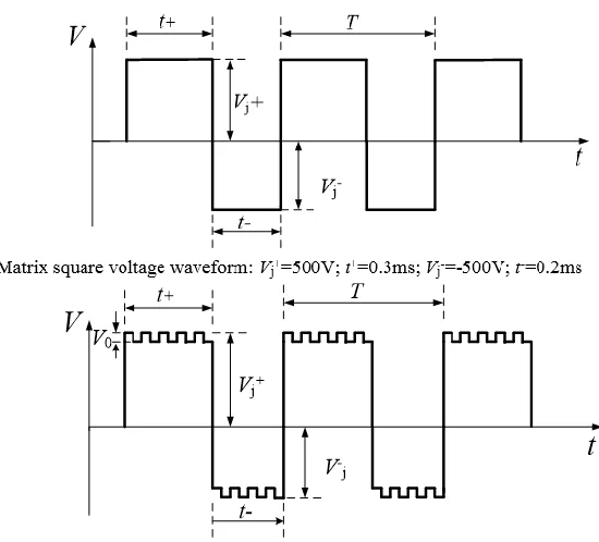
Figure 1. Oscillograms of the PEO films coated on Al alloy by different modes: (a) custom pulse voltage mode; (b) transient self-feedback control mode.
[image:2.596.164.439.384.633.2]
degreased ultrasonically in acetone, and then cleaned with distilled water. The composition of 2024 Al alloy was (wt. %): Mg 1.2-1.8, Zn 0.25, Ti 0.15, Mn 0.3-0.9, Cr 0.10, Cu 3.8-4.9, Si 0.50, Fe 0.50 and Al balance.
Two specimens were processed using a 100 kW pulse power supply (DuercoatⅣ) in conjunction with stirring and cooling systems. This power supply was used to deliver different voltage waveforms: custom pulse voltage mode and transient self-feedback control mode. The custom pulse voltage mode in Fig. 1(a) was used to prepare the traditional PEO film (designed as T-PEO). The transient self-feedback control mode in Fig. 1(b) was used to prepare a compact PEO film (designed as C-PEO). The PEO electrolytes composition comprised of sodium hydroxide (3-5 g/L) and sodium silicate (2-5 g/L). A two-electrode cell (a graphite electrode and a Al electrode) was used for the PEO treatment and a cooling system kept the electrolyte temperature below 35℃.
2.2. Characterizations
PEO discharge processes and macroscopical surface morphologies of the PEO films were indicated by optical photographs with a digital camera (PowerShot G3X, Canon). Cross-sectional and surface morphologies of the PEO films were observed by scanning electron microscopy (SEM) in a Hitachi S-4700 system. Before imaging, Au was firstly sputtering on the sample. An accurate element analysis was investigated by electron probe microanalysis (EPMA, JEOL JXA-8500F), equipped 5 wavelength dispersive X-ray spectroscopy (WDS, Oxford INCA X-Act). Spot scans were carried out at 20 kV and 10nA.Surface phase distribution of the PEO films were preformed using a X-ray diffractometer (XRD, X’ Pert PRO MRD) with Cu Kα radiation. The 2θ geometry was in the ranges of 20-80°with 0.02°size step. The α-Al2O3 constituent of the film was used as a research object, the residual stresses were measured by LXRD laboratory residual stress and retained austenite measurement systems based on X-ray diffraction sin2ψmethod [14]:
0 2
π 2
2 1 180
( ) cot
( ) (sin )
E
(1)
where θ0 is the Bragg’s angle for the samples without residual stresses, θ is the Bragg’s angle for the samples with residual stresses, υ is Poisson’s ratio and E is Young’s modulus of the thin film. υ and E for alumina were taken at υ =0.220 and E=200 GPa [14, 15]. And PROTO XRD Win 2.0 software was used to calculate the residual stress value, which has advanced peak fitting functions and provides abundant information of breadth, FWHM, and sin2ψ plots.
3. RESULTS
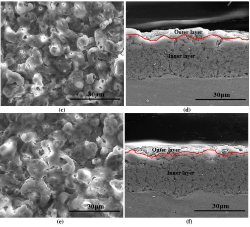
representative regions were further studied by SEM. Fig. 3 displays the SEM images of the T-PEO films at four regions (designed as Region 1-4). As shown in Fig. 3(a) and (c), many coarse ceramic particles, large pores, concentrated cracks can be seen on the T-PEO film surface at Regions 1 and 2. The cross-section images in Fig. 3(b) and (d) exhibit a bilayer. Meantime, the appearance of some big pores (5-10 μm in diameter) in the outer layer are detrimental for film compactness, which results in different thicknesses of 10-15μm and 3-10 μm for the inner layers at Regions 1 and 2, respectively. Regions 3 and 4 are at relatively smooth region as shown in Fig. 2(b).
(a) (b)
(c) (d)
Figure 2. Optical photographs of (a) discharge process and (b) surface morphology of T-PEO film; optical photographs of (c) discharge process and (d) surface morphology of C-PEO film.
1cm 1cm
3
1
2
4
1cm
1
2
3
[image:4.596.67.531.213.701.2]
Large and coarse scattered ceramic particles still overlay of each other and randomly distribute on the surface morphologies of Regions 3 and 4 in Fig. 3(e) and (g). But the bilayers from the cross-section image in Fig. 3(f) and (h) are different from those of Regions 1 and 2: the outer layers contain cavities and pores with the thickness of 10-12 μm, while the inner layers present relatively compact with the thickness of 20-25 μm. Based on the morphologies of four regions, the uneven distribution of the bilayer, the overlap of large and coarse scattered ceramic particles, and the obviously penetrable microdefects of cracks and pores are the main factors of structural failure and poor compactness. According to the smooth feature of macro-profile in Fig. 2(d), three regions (designed as Region 1-3) were selected and their morphologies were shown in Fig. 4. From the SEM images of surface morphologies in Fig 4 (a) (c) and (e), a compact appearance with a relatively uniform scattering of the small ceramic particles can be observed. There were only a few pores that were distributed homogeneously in the C-PEO films, with a size range of 2-5 μm. Even though small amount of cracks were found in Fig. 4(a), this has no effect on the film compactness.
(a) (b)
(e) (f)
(g) (h)
Figure 3. SEM images of surface and cross-section morphologies of T-PEO film: (a)(b)Region 1; (c)(d) Region 2; (e)(f) Region 3; (g)(h) Region 4.
[image:6.596.73.523.69.479.2]
(c) (d)
(e) (f)
Figure 4. SEM images of surface and cross-section morphologies of C-PEO film: (a)(b)Region 1; (c)(d) Region 2; (e)(f) Region 3
From the cross-sectional morphologies of the C-PEO film in Fig. 4(b) (d) and (f) it can be seen that the outer layers are integrated, no obviously penetrable microdefects, such as big cracks and pores can be observed in the outer layer, and their average thicknesses are only about 3-5 μm. For the inner layers of the three regions, their compactness and homogeneity are almost the same with the naked eye, and the thicknesses of the three regions are all about 23-27 μm. Based on the morphologies of three regions, the relatively uniform scattering of the small ceramic particles, the lack in the penetrable microdefects of big cracks and pores, and the even distribution of the bilayer provides good ways of forming compact and stable bilayer.
[image:7.596.51.547.68.520.2]
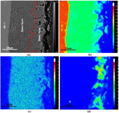
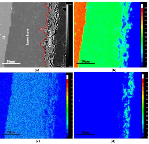
Because the bilayer at Regions 1 and 2 of the T-PEO film are incomplete based on the Fig. 3, Regions 3 and 4 of the T-PEO film were selected for test regions as shown in fig.5 and fig.6 which can guarantee the accurate element distribution; while Region 1 of the C-PEO film was chosen as the test region due to the similar bilayer of the cross-sections (fig. 4) as shown in Fig.7. It can be seen from the T-PEO film (fig. 5 and fig.6) that Al and O are in all the film regions.
(a) (b)
(c) (d)
Figure 5. EPMA of T-PEO film coated on Al substrate at Region 3 formed in NaOH-Na2SiO3 electrolyte: (a) SEM, (b)Al, (c) O, (d) Si.
[image:8.596.57.541.181.642.2]
reduces or even disappears. Al and O are again present in all regions of C-PEO film material. Notably, the thickness of the Si-rich layer, concentrated at the outer layer, is greatly reduced to 3-9 μm under the densification effect.
(a) (b)
(c) (d)
Figure 6. EPMA of T-PEO film coated on Al substrate at Region 4 formed in NaOH-Na2SiO3 electrolyte: (a) SEM, (b)Al, (c) O, (d) Si.
[image:9.596.52.538.143.615.2]
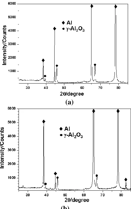
(113) plane at 2θ=43.363°, γ-Al2O3 (400) plane at 2θ=45.863°). The intensity ratio (Iα/Iγ) of different regions for the T-PEO and C-PEO films are shown in Table 1. For Regions 1 and 2 of the T-PEO film, the intensity ratio values (Iα/Iγ) cannot be calculated attributed to insufficient α-Al2O3 peak intensities. The Iα/Iγ values for the T-PEO film at Regions 3 and 4 are 0.725 and 0.573, showing a relatively high content of α-Al2O3 phase. For the C-PEO film, it is found that the Iα/Iγ values obtained under high frequency carrier waveform (transient self-feedback control mode) are all in the range of 0.13–0.15. It is reported that residual stresses can affect various properties of PEO films, e.g. adhesion, hardness, fatigue crack propagation and wear resistance. In this paper, residual stress was measured using the diffracted peak at 2θ=152.98° at high-angle diffraction range to ensure a higher measuring accuracy. The tests were employed in the ψ angle ranges of -38.5°-11.5° with 0.01° size step (2θ). The residual stress values calculated by PROTO XRD Win 2.0 software are shown in Table 2.
(a) (b)
(c) (d)
[image:10.596.74.523.281.709.2]
Table 1. Content ration of α-Al2O3 to γ-Al2O3 (Iα/Iγ) in the T-PEO and C-PEO films.
Region(T-PEO) 1 2 3 4
Iα/Iγ — — 0.752 0.573
Region(C-PEO) 1 2 3
[image:11.596.188.410.407.761.2]Iα/Iγ 0.136 0.157 0.142
Table 2. Residual stress values of the T-PEO and C-PEO films
Region 1 2 3 4
T-PEO(MPa) -128.22±18.42 -110.01±6.20 -50.85±11.66 -87.72±9.72
Region 1 2 3
C-PEO(MPa) 18.48±5.71 22.52±6.39 29.76±9.70
As shown in Table 2, the residual stresses evaluated for the T-PEO film at different regions are found to be compressive and exhibits variance. The compressive stresses in Regions 1 and 2 are much bigger than those in Regions 3 and 4, indicating the heterogeneous phase distribution. For the C-PEO films, it is found that small and consistent residual stress values in all the regions display good characteristic of the C-PEO film.
(a)
(c) Iα/Iγ=0.725
(d) Iα/Iγ=0.573
Figure 8. XRD patterns of T-PEO film at different regions: (a) Region 1; (b) Region 2; (c) Region 3; (d) Region 4.
4. DISCUSSION
4.1. Formation mechanism of film compactness
[image:12.596.177.419.83.480.2]
distributes at the lower resistance micro-field of the inner layer. These micro-fields gradually evolve into microdefects under the continuous action of impact current. In the meantime, the conductivity and the capacitance of the microdefects are also increased greatly. These huge residual discharge energies of impact current are vigorous but unstable, they continue to accumulate in the micro-field of microdefects or the coarse discharge channels during the dielectric barrier discharge process. Finally, these energies are released in the form of the concentrated spark discharge and sprayed outside the discharge channels. This process presents ―volcano eruptions‖ phenomenon on the sample surface of some concentration areas. After this concentrated discharge process, the original discharge channels become much coarser and bigger to form the characteristic morphology of ―volcano (see fig. 3(a) and (c))‖, micro-crack and pores are more concentrated near the ―volcano‖, the ceramic particles grow faster and become abnormally bulky (see fig. 3(e) and (g)). For the C-PEO process, the tiny sparks as shown in Fig. 2(c) were distributed uniformly on the surface instead of the concentrated, strong spark discharge, that is, the accumulation and release of huge residual energies (impact current) are inhibited by the high frequency carrier waveform, which avoids outer layer destruction and film compactness influence. So it can be seen that the big microdefects (volcano, cracks) and large PEO ceramic particle concentration seldom occur on the C-PEO film surface (see fig. 4), the high frequency carrier waveform produces a remarkable effect on the C-PEO film compactness.
EPMA readily discloses the element distribution (Si, Al and O) in the PEO film. It can be seen from figs. 5-7 that the distribution region of the silicon-rich layer roughly equals to the outer layer of the bilayer, so it also can reflect the generation of the outer layer. The concentrated energy discharge is easy to occur in the region of microdefects, such as Region 3 of the T-PEO film (see fig. 3(f) and fig. 5(a)). The discharge process one hand will increase the growth of the T-PEO film in this region, on the other hand it can destroy the newly formed film. During the T-PEO process the two sub-effects are constantly intersecting, which results in the poor compactness of the outer layer. For the compact Region 4, it usually can avoid the concentrated large energy discharge, but the slow growth reduces the outer layer thickness (see fig.3(h) and fig.6(a)). Overall, the different growth rate of the outer silicon-rich layer leads to its poor compactness. In contrast, the uniform energy discharge of the C-PEO film ensures the consistency of outer film thickness and the increase of film compactness (see figs. 4(b) (d) (f) and fig. 7).
4.2. Formation mechanism of microstructure uniformity
in the following T-PEO film growth, which means a cycle of destruction in the PEO film microstructure and compactness. In the meantime, high plasma sintering energy can also promote the mullite formation and result in the generation of larger cracks and defects. In turn, these cracks and defects near mullite region further aggravate inhomogeneous plasma discharge and damage T-PEO film compactness. Therefore, unordered α-Al2O3 grain growth and mullite phase formation are the important factors to destroy T-PEO microstructure. By contrast, the high-frequency carrier waveform of the C-PEO film inhibits concentrated plasma discharge, ensures ordered grain growth and prevents the mullite formation. These advantages basically stop the crack and defect generation and improve obviously the C-PEO film compactness and microstructure uniformity.
5. CONCLUSION
(1) The C-PEO film displayed a compact appearance with a relatively uniform scattering of the small ceramic particles, and a stable bilayer of a lack in the penetrable microdefects of big cracks and pores.
(2) For the C-PEO process, the tiny sparks were distributed uniformly on the C-PEO film surface instead of the concentrated, strong spark discharge. The accumulation and release of huge residual energies were inhibited by the high frequency carrier waveform, which avoided outer layer destruction and film compactness influence.
(3) The high-frequency carrier waveform reduced the α-Al2O3 content in the C-PEO film, obtained uniform phase distribution, and eliminated the residual stress obviously.
ACKNOWLEDGEMENT
This work was supported by project supported by National Natural Science Foundation (51402307).
References
1. W. Xue, Z. Deng, Y. Lai, R. Chen, J. Am. Ceram. Soc., 81 (1998) 1365. 2. W. Xue, Z. Deng, R. Chen, T. Zhang, Thin Solid Films, 372 (2000) 114.
3. C.S. Dunleavy, I.O. Golosnoy, J.A. Curan, T.W. Clyne, Surf. Coat. Technol., 203 (2009) 3410. 4. E. Matykina, R. Arrabal, P. Skeldon, G.E. thomson, P. Belenger, Surf. Coat. Technol., 205 (2010)
1669.
5. R.O. Hussein, X. NIe, D.O. Northwood, Surf. Coat. Technol., 205 (2010) 1659. 6. A.V. Timoshenko, Y.V. Magurova, Surf. Coat. Technol., 199 (2005) 135.
7. A.L. Yerokhin, A. Shatrov, V. Samsonov, P. Shashkov, A. Pilkington, A. Leyland, A. Mathews, Surf. Coat. Technol., 199 (2005) 150.
8. K.Q. Du, X. H. Guo, Q. Z. Guo, F. H. Wang, Y. Tian, Mater. Lett., 91 (2013) 45.
9. K.Q. Du, X. H. Guo, Q. Z. Guo, R. Wang, F. H. Wang, Y. Tian, J. Electrochem. Soc., 159 (2012) C597.
10. X. H. Guo, K.Q. Du, Q. Z. Guo, Y. Wang, F. H. Wang, ECS Solid State Lett., 2 (2013) S1. 11. X. H. Guo, K.Q. Du, Q. Z. Guo, Y. Wang, F. H. Wang, ECS Electrochem. Lett., 2 (2013) C1. 12. X. H. Guo, K.Q. Du, Q. Z. Guo, Y. Wang, F. H. Wang, Electrochem. Commun., 28 (2013) 95. 13. X. H. Guo, K.Q. Du, Q. Z. Guo, Y. Wang, F. H. Wang, Int. J. Hydrogen Energy, 38 (2013) 16387. 14. R.H.U. Khan, A.L. Yerokhin, T. Pilkington, A. Leyland, A. Matthews. Surf. Coat. Technol., 200
(2005) 1580.
15. A.A. Voevodin, A.L. Yerokhin, V.V. Lyubimov, M.S. Donley, J.S. Zabinski. Surf. Coat. Technol., 86–87 (1996) 516.
16. L. Lia, S. Lanteri, R. Perrussel. J. Comput. Phys., 256 (2014) 563. 17. J. Kovác̆ik, F. Simanc̆ı́k, Scripta Mater., 39 (1998) 239.
18. F. Jaspard-Mécuson, T. Czerwiec, G. Henrion, T. Belmonte, L. Dujardin, A. Viola, J. Beauvir, Surf. Coat. Technol., 201 (2007) 8677.
19. Y. J. Guan, Y. Xia, G. Li, Surf. Coat. Technol., 202 (2008) 4602.
20. E. Matykina, R. Arrabal, P. Skeldon, G.E. Thompson, Electrochim. Acta, 54 (2009) 6767. 21. A. Melhem, G. Henrion, T. Czerwiec, J.L. Briançon, T. Duchanoy, F. Brochard, T. Belmonte,
Surf. Coat. Technol., 205 (2011) S133.
100.
23. Y. L. Cheng, Z. G. Xue, Q. Wang, X. Q. Wu, E. Matykina, P. Skeldon, G. E. Thompson, Electrochim. Acta, 107 (2013) 358.
24. H. Schaper, L.L. Van Reijen, Thermochim Acta, 77 (1984) 383.
25. G. Lv, W. Gu, H. Chen, W. Feng, M.L. Khosa, L. Li, E. Niu, G. Zhang, S. Yang, Appl. Surf. Sci., 253 (2006) 2947.
26. H.Wu, Z. Jin, B. Long, F. Yu, X. Lu, Chin. Phys. Lett., 20 (2003) 1815.
27. W.C. Gu, G.H. Lv, H. Chen, G.L. Chen, W.R. Feng, G.L. Zhang, S.Z. Yang, J. Mater. Process Technol., 182 (2007) 28.
28. M. Bodaghi, A.R. Mirhabibi, H. Zolfonun, M. Tahriri, M. Karimi, Phase Transit., 81 (2008) 571. 29. S. Sembiring, W. Simanjuntak, Makara J. Sci., 16 (2012) 77.
30. C. Gerardin, S. Sundaresan, J. Benziger, Chem. Mater., 6 (1994) 160.
31. M.A. Sainz, F.J. Serrano, J.M. Amigo, J. Bastida, A. Caballero, J. Eur. Ceram. Soc., 20 (2000) 403.
32. Residual Stress Measurement by X-ray Diffraction, Society for Automotive Engineering, (1971), USA.
33. ASM Handbook, Surface Engineering, vol. 5, ASM International, (1999), USA. 34. J. Tian, Z. Luo, S. Qi, X. Sun, Surf. Coat. Technol., 154 (2002) 1.