Abstract This paper encloses a 2T MUX to reduce the transistor count in single bit adder element to 6. It uses HEP-1 tool in MENTOR GRAPHICS to compare parameters like Power, delay, PDP, and ADP with 8TEXOR, 8TMUX, 6T adder etc. with 1.2V supply voltage in 130-nm technology. The proposed one presents an improvement of 51%, 98% in ADP and PDP respectively when compared to the 8T MUX based Single bit adder element. Further, it emphasizes low power dissipation and minimum delay required to exhibit the desired logic that is useful in many portable applications.
Index Terms: single bit adder element, 8TMUX, 2TMUX, MUX Area Delay Product (ADP), Power Delay Product (PDP).
I. INTRODUCTION
Single bit adder elements are the kernel components in many modern hardware circuits and constitutional blocks of VLSI circuits. Several enhancements have done to its structure from its invention. The enhancements include transistors count, power, delay, area, PDP, ADP to exhibit the desired logic. The major advantage of reducing the transistor count is to fabricate many devices on a single chip that minimizes the total area. Recently, the use of portable electronic gadgets is increased exponentially. The main theme behind these portable electronic gadgets is enhanced power, delay, area, PDP and ADP. Research efforts in this field of VLSI has many folds to attain these objectives. Also, package density increases as the transistor count on silicon chip increases [1]. As package density increases, area and power increases that leads to packaging, cooling cost problems. Hence, low power less delay, minimum area requirements are the efficient design consideration in portable electronic gadgets.
Single bit adder element has A, B, C as inputs and outputs are SUM, CARRY. The logical operation of this single bit adder element is implemented with EXOR gate, AND gates and OR gates. The logic for SUM requires EXOR gate while the logic for CARRY requires EXOR with AND, OR gates [1], [2], [3]. The basic logical expressions for outputs SUM and CARRY of a single bit adder element are
Revised Manuscript Received on April 18, 2019.
K V K V L Pavan Kumar, Asst.prof, Electronics & Communication Engineering, Koneru Lakshmaiah Educational Foundation, Vaddeswaram, India.
G L Sravanthi, Asst.prof, Computer Science & Engineering, Vignan’s Nirula Institute of Technology & Science for Women, Guntur, India.
N Suresh Kumar, Asst.prof, Electronics & Communication Engineering, Koneru Lakshmaiah Educational Foundation, Vaddeswaram, India.
V S V Prabhakar CISCO Chair at IIDT (International Institute of Digital Technologies), Tirupati, India.
SUM = A B C (1) CARRY = AB + BC + CA (2)
The basic schematic diagram of single bit adder element is represented below in figure1.
Fig1. Single bit adder element (full adder) Section II describes some prominent existing single bit adder elements, 8T MUX based single bit adder element [5], [6] Section III proposes the 6T MUX based single bit adder element with six transistors, Section IV provides the comparison of 6T single bit adder element with temperature and comparison of power, delay, area delay product and power delay product between 8T MUX and 6T MUX based single bit adder element, Section V concludes the paper.
II. PRIOR ART
The single bit adder element mentioned above is designed by using 32 transistors (both PMOS & NMOS) in conventional manner [1],[2]. From [4],[6] single bit adder elements are designed by using 8 transistors Single bit adder elements are implemented by using EXOR & MUX configuration and by using MUX configurations only with the help of 8 transistors. The former [4] single bit adder element uses 3 transistors to design an EXOR. Two EXOR gates are used to implement SUM and one EXOR, one MUX function to implement CARRY respectively. SUM & CARRY outputs are obtained by using equations (1) & (2). To obtain SUM, the inputs to the EXOR function are A, B to produce the output and this is applied as an input to the second EXOR having the other input C to obtain respective output. To obtain CARRY, the inputs to the EXOR function are A, B to produce the output and this is applied as selection line input to the 2TMUX having the other inputs C & CBAR for the transistors to obtain respective output.
Performance Analysis of 6Transistor Single bit
Adder Element
The later [6] single bit adder element uses 2 transistors to design MUX and 2 transistors to design an INVERTER. The outputs SUM & CARRY are produced with the help of three 2TMUXes and one INVERTER respectively. An extra output called CARRYBAR is produced with the two outputs SUM & CARRY. SUM is obtained by using two 2TMUXes and an INVERTER in which the first MUX uses selection line A and the inputs to it are C & CBAR to produce the EXOR function and is applied as the selection line input to the second 2TMUX, the other inputs to this 2TMUX are B and CARRYBAR. CARRY is obtained by using two 2TMUXes and an INVERTER in which the first MUX uses selection line A and the inputs to it are C & CBAR to produce the EXOR function and is applied as the selection line input to the third 2TMUX, the other inputs to this 2TMUX are B and A. As compared with the existed designs of single bit adder elements the proposed method provides reduced transistor count, minimum delay, low power, maximum throughput.
III. PROPOSED METHOD
A 2 transistor MUX has been proposed using both PMOS and NMOS transistors to produce SUM and CARRY in the implementation of adder element [1]. MUX is a digital combinational logic circuit used to produce the output from one of the inputs based on the selection lines. MUX contains many input data lines and only one output data line where the input data lines are in the order of 2n, where n represents the number of selection lines, 2n is the number of inputs respectively [4], [5]. Depending on the n value, MUX is available in many variants like 2 to 1 MUX,4 to 1 MUX,8 to 1 MUX,16 to 1 MUX with one two, three and four selection lines respectively. MUX provides switching operation between input and output with the help of selection lines. MUX directs the input to the output with the aid of selection line where the selection line acts as a control line input in the operation of MUX. It is also called as data selector because it selects the input data line with the help of selection line to the output line. MUX is implemented with the help of transistors at the circuit level that depends on its size. In this context, a 2T MUX is designed to implement a single bit adder element that requires a single PMOS and single NMOS transistors [5] as in below figure2.
Fig2. 2T MUX
A 2T MUX consists of three input lines and one output line in which A and B are input data lines, SEL is a control selection line and OUT is the data output data line respectively. From the circuit when the SEL line is zero, PMOS transistor gets turned ON and NMOS transistor gets turned OFF that provides a short circuit path from A to OUT through PMOS and open circuit path from B to OUT through NMOS respectively. Therefore, MUX selects input data line A to the output data line OUT. when the SEL line is one, PMOS transistor gets turned OFF and NMOS transistor gets turned ON that provides a open circuit path from A to OUT through PMOS and short circuit path from B to OUT through NMOS respectively [6], [7]. Therefore, MUX selects input data line B to the output data line OUT. SEL line carries either logic ‘0’ or logic ‘1’ from the respective input data lines to the output lines. Single bit adder element with 2T MUX is designed as in below figure, in which it consists of three 2 to 1 MUX’s implemented with two transistors (one PMOS and one NMOS) in each MUX. It is subdivided into three sections as MUX 1, MUX 2, and MUX 3 in which MUX 1 &3 sections produces SUM and MUX 1,2 &3 produces CARRY respectively. Single bit adder element implemented with 2T MUX produces SUM and CARRY by using the Boolean expressions as
SUM = A B C CARRY = C. (A B A.B
By using the above Boolean expressions, a switch level schematic is implemented in below figure organized with 2T MUX’s. From the circuit diagram, single bit adder element is implemented with a total of six transistors, in which they contain three sections of MUX [5],[6]. Where each MUX consists of one PMOS and NMOS transistors with a total of three PMOS & NMOS transistors respectively as in figure3 below Implementation of single bit adder element uses both true and complementary inputs to produce SUM and CARRY. The complementary inputs are obtained by using an inverter. The circuit shown below is represented without inverters. In MUX 1 section the input data lines to the MUX are A and ABAR with control selection line B to produce output as A B [4], [5]. In MUX 2 section the input data lines are A and C with control selection line as A B to produce output CARRY [5],[6]. In MUX 3 section the input data lines are C and CBAR with control selection line A B to produce SUM. Therefore, Single bit adder element uses the MUX logic to produce SUM and CARRY. Single bit adder element uses two control selection lines B and A B in section MUX 1 and MUX 2 & 3 respectively [7],[8]. In this context, with respect to MUX 1, when B=logic’0’=BBAR, it selects input data line A and when B=logic ‘1’=B, it selects input data line ABAR that produces output in the equation described as
OUT= A B= BBAR.A+B. ABAR
Similarly, with respect to MUX 2, A B acts as the control selection line, when A B = logic’0’= (A B)’ it
PM OS
NM OS
A
B
selects input data line A and when A B = logic’1’= A B it selects input data line C that produces output CARRY [7], [8]as described below
CARRY = C. (A B A.B
Also, with respect to MUX 3, A B acts as the control selection line, when A B = logic’0’= (A B)’ it selects input data line C and when A B = logic’1’= A B it selects input data line CBAR that produces output SUM as described below
SUM = A B C
[image:3.595.311.544.52.194.2]Fig3. 6T single bit adder element The transistors lengths and widths in the above schematic diagram are depicted in the below table I.
Table I Lengths & Widths of the MOS Transistors (PMOS & NMOS)
MUX Transistor Width Length
MUX 1 PMOS 260 130
NMOS 180
MUX 2 PMOS 260 130
NMOS 180
MUX 3 PMOS 260 130
NMOS 180
To obtain the perfect logic levels, the widths of the transistors for NMOS in MUXes 1, 2 & 3 satisfy width to length ratio as 1.5:1 to obtain the perfect logic ‘0’. The widths of the transistors for PMOS in MUX 2 & 3 satisfy the width to length ratio as 2:1 to obtain the perfect logic ‘1’.
IV. RESULTS&DISCUSSION
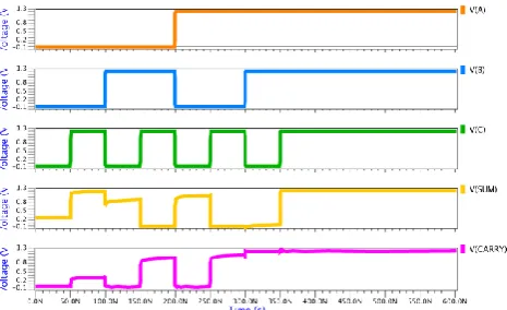
The results for 6T MUX based single bit adder element is shown in figure that corresponds to a conventional full adder where it has three inputs as A, B, C and outputs SUM, CARRY respectively. The inputs are applied in such a way that A=00001111, B=00110011, C=01010101.The observed outputs of SUM =01101001 and CARRY=00010111. In the figure4 shown, the supply voltage applied is 1.2V, hence the inputs and outputs have 0V as logic level ‘0’ and 1.2V as logic level’1’ respectively.
Fig 4. Output waveform of a 6Transistor single bit adder element
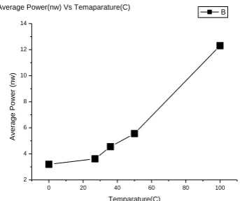
The power and delay of 6TMUX based single bit adder element are varied with respect to variations in temperature from 0 to 150 degrees as represented in the below table that provides significant changes in power, delay values. The power that is measured is the average power measured in nano watts and the delay is computed from inverting mode measured in pico seconds. Power delay product is obtained by multiplying power with delay measured in atto joules. The power that is obtained is the average power dissipation evaluated from the output waveforms depending on the input stimulus vector. Delay that is obtained is the total propagation delay or time taken for the input to produce the respective output. Power delay product is the product of the average power & propagation delay. The performance of the proposed single bit adder element is compared at various temperatures varying from 0 degrees to 100 degrees centigrade in terms of delay, average power, power delay product and area delay product respectively as in table below.
Table II Comparison pf Power, Delay & PDP with temperature (C)
Temperature (Degrees C)
Avg Power
(nW)
Delay (ps) PDP (aJ)
0 3.196 254.80 0.814
27 3.619 250.18 0.905
36 4.550 249.19 1.133
50 5.552 248.00 1.376
100 12.304 245.45 3.020
[image:3.595.308.548.457.576.2]0 20 40 60 80 100 2
4 6 8 10 12 14
Average Power(nw) Vs Temaparature(C)
Aver
ag
e Pow
er
(n
w)
Temparature(C)
B
Fig 5. Comparison of average power with temperature The variation of delay with temperature is in below figure6. From the graph, delay is evaluated at certain temperatures from 0 to100 and plotted accordingly. From the graph, it is clear that the delay decreases with rise in temperature.
Fig 6. Comparison of delay with temperature
The variation of PDP with temperature is in below figure7. From the graph, Power Delay Product is evaluated at certain temperatures from 0 to100 and plotted accordingly.
Fig 7. Comparison of PDP with temperature
The table below provides the comparison between different single bit adder elements designed with various transistor
scaled down to 6 transistors [1], [4], [9]. The performance of these single bit adder elements is evaluated with parameters like power, delay, PDP and ADP espectively.
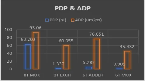
Table III.Comparison of PDP & ADP of different designs Design
of one-bit
adder
TC Delay
(ps)
Avg power
(nw)
PDP (aJ)
ADP (um2ps)
8T MUX 8 406.74 155.39 63.203 93.06
8T EXOR 8 262.48 5.0970 1.337 60.055
6T ADDER 6 422.09 12.514 5.282 76.651
6T MUX 6 250.18 3.619 0.905 45.432
The table below provides technology comparison of six transistor single bit adder element between 130,90, & 60nm with the supply voltages 1.2V,1.0V &1.0V respectively.
Table IV.Comparison of Power, Delay & PDP with Technology
Technology Supply voltage
Avg power
(nw)
Delay (ps)
PDP (aJ)
130 1.2V 3.619 250.18 0.905
90 1.0V 5.358 136.97 0.733
60 1.0V 19.239 230.31 4.430
It is observed that the average power dissipation is varied from 3.619nw to 19.239nw with technology from 130nm to 60nm respectively. The delay is varied from 250.18ps to 230.31ps with technology from 130nm to 60nm respectively. Hence, power delay product is varied from 0.905aJ to 4.430aJ with technology from 130nm to 60nm respectively. The variation of delay with respect to temperature is in below figure7. From the graph, Power Delay Product is evaluated at certain temperatures from 0 to100 and plotted accordingly A comparison between delay and power for a single bit adder element is depicted in the below figure8 with respect to their transistor counts and configuration.
Fig 8. Comparison of delay & Power of 6T single bit adder element
[image:4.595.82.254.60.204.2] [image:4.595.308.549.510.668.2] [image:4.595.64.273.551.731.2]or-2 Photo
A comparison between PDP and ADP for a single bit adder element is depicted in the below figure9 with respect to their transistor counts and configuration.
Fig 9. Comparison of PDP & ADP of 6T single bit adder element
From the graph, it is clear that PDP & ADP of the 6TMUX based single bit adder element is minimized compared with 8TMUX, 8TEXOR configurations. Therefore, 6TMUX based single bit adder element is an efficient one-bit adder element in terms of power, delay, PDP & ADP.
V. ONCLUSION
Single bit adder element designed with 6 transistors using MUX based logic provides improvement in terms of power, delay, PDP and ADP respectively. Therefore, 6T MUX based single bit adder element minimizes the power, by 97% delay by 38%, ADP by 51% and PDP by 98% at 27-degree temperature compared with 8T MUX based single bit adder element respectively. It also provides significant variations in power, delay, and PDP for a 6T MUX based single bit adder element with variations in temperatures from 0 to 100 degrees. A significant improvement in power, delay and PDP is obtained at 0- and 27-degree temperatures.
REFERENCES
1. S. Kang and Y. Leblebici, “CMOS Digital Integrated Circuits-Analysis and Design”, McGraw-Hill, 2003.
2. Rabaey J.M., Chandrakasan A., and Nikolic B., Digital Integrated Circuits, A Design Perspective, Englewood Cliffs, N.J.: Prentice Hall, 2nd ed,2002.
3. PUCKNELL, D.A. Basic VLSI Design, 3rd ed. New Delhi (India): Prentice-Hall of India Pvt. Limited, 1994. ISBN: 9788120309869.
4. BHATTACHARYYA, P., KUNDU, B., GHOSH, S., et al.
Performance analysis of a low-power high-speed hybrid 1-bit full adder circuit. IEEE Transactions on very large-scale integration (VLSI) systems, Oct. 2015, Vol. 23, no. 10, p. 2001-2008. DOI: 10.1109/TVLSI.2014.2357057.
5. MOHANTY, B.K., PATEL, S.K. Area–delay–power efficient carry-select adder. IEEE transactions on circuits and systems II: express briefs, Jun. 2014, Vol. 61, no. 6, p. 418-422. DOI: 10.1109/TCSII.2014.2319695.
6. Yi WEI, Ji-Zhong SHEN Design of a novel low power 8-transistor 1-bit full adder cell Journal of Zhejiang University-SCIENCE C (Computers & Electronics) ISSN 1869-1951 (Print); ISSN 1869-196X (Online).
7. Ahmed M. Shams, T. Darwish, and M. Bayoumi, “Performance analysis of low power 1-bit CMOS full adder cells,” IEEE Trans. Very Large Scale Integr. (VLSI) Syst., vol. 10, no. 1, pp. 20–29, Feb. 2002. 8. V.V. Shubin “New CMOS circuit implementation of a 1-bitfull adder
cell” Russian Microelectronics, Vol. 40, No. 2, pp. 130-139, 2011. 9. T. Venkata Rao and A. Srinivasulu "Modified level restorers using
current sink and current source inverter structures for BBL-PT full adder", Radio engineering, vol. 21, no. 4, pp. 1279–1286,2012.
AUTHORSPROFILE
K V K V L Pavan Kumar, is pursuing his Ph.D. in the stream of VLSI design at K L Deemed to be University He completed his MTech in VLSI Design at VIGNAN University and published several articles in Scopus on VLSI.
G L Sravanthi, is working as an Assistant professor in the department of Computer Science & Engineering, at Vignan’s Nirula Institute of Technology & Science for Women, Guntur. She completed her MTech in Computer Science & Engineering at VIGNAN University and
published several articles in Scopus on VLSI.
N Suresh Kumar, is pursuing his Ph.D. in the stream of Speech processing at K L Deemed to be University He completed his MTech in Communications & Signal Processing at PVP Siddhartha engineering college and published several articles in Scopus on Signal Processing. .
[image:5.595.49.293.86.219.2]