This is a repository copy of Imaging of interlayer coupling in van der Waals heterostructures using a bright-field optical microscope.
White Rose Research Online URL for this paper: http://eprints.whiterose.ac.uk/110371/
Version: Accepted Version
Article:
Alexeev, E.M. orcid.org/0000-0002-8149-6364, Catanzaro, A., Skrypka, O.V. et al. (8 more authors) (2017) Imaging of interlayer coupling in van der Waals heterostructures using a bright-field optical microscope. Nano Letters, 17 (9). pp. 5342-5349. ISSN 1530-6984 https://doi.org/10.1021/acs.nanolett.7b01763
[email protected] https://eprints.whiterose.ac.uk/
Reuse
Items deposited in White Rose Research Online are protected by copyright, with all rights reserved unless indicated otherwise. They may be downloaded and/or printed for private study, or other acts as permitted by national copyright laws. The publisher or other rights holders may allow further reproduction and re-use of the full text version. This is indicated by the licence information on the White Rose Research Online record for the item.
Takedown
If you consider content in White Rose Research Online to be in breach of UK law, please notify us by
Imaging of interlayer coupling in van der
Waals heterostructures using a bright-eld
optical microscope
Evgeny M. Alexeev,
∗,†Alessandro Catanzaro,
†Oleksandr V. Skrypka,
†Pramoda
K. Nayak,
‡Seongjoon Ahn,
‡Sangyeon Pak,
¶Juwon Lee,
¶Jung Inn Sohn,
¶Kostya S. Novoselov,
§Hyeon Suk Shin,
‡and Alexander I. Tartakovskii
∗,††Department of Physics and Astronomy, University of Sheeld, Sheeld S3 7RH, UK
‡Department of Energy Engineering and Department of Chemistry, Ulsan National Institute
of Science and Technology (UNIST), 50 UNIST-gil, Ulsan 44919, Republic of Korea
¶Department of Engineering Science, University of Oxford, Oxford OX1 3PJ, UK
§School of Physics and Astronomy, University of Manchester, Oxford Road, Manchester M13 9PL, UK
E-mail: [email protected]; [email protected]
Abstract
interfaces. Here, we demonstrate an ecient method for monitoring interlayer coupling in heterostructures made from transition metal dichalcogenides using photolumines-cence imaging in a bright-eld optical microscope. The colour and brightness in such images are used here to identify mono- and few-layer crystals, and to track changes in the interlayer coupling and the emergence of interlayer excitons after thermal annealing in mechanically exfoliated akes as well as a function of the twist angle in atomic layers grown by chemical vapour deposition. Material and crystal thickness sensitivity of the presented imaging technique makes it a powerful tool for characterisation of van der Waals heterostructures assembled by a wide variety of methods, using combinations of materials obtained through mechanical or chemical exfoliation and crystal growth.
Keywords
Introduction
Atomically thin materials oer a new paradigm for control of electronic excitations in the extreme two-dimensional (2D) limit in condensed matter. Recently this concept has been developed further with the creation of 2D heterostructures in which individual atomic layers are held together by van der Waals (vdW) interaction.14The weak interlayer bonding loosens the lattice matching requirement, allowing a wide range of materials to be used in one device. Such vdW heterostructures combine unique properties of 2D materials with transparency and extreme exibility, allowing a range of novel electronic and optoelectronic devices to be fabricated. Indeed, a wide variety of such devices has been demonstrated, including eld-eect transistors,3,59 light emitting devices,1013 vertical tunneling transistors1417 and photodetectors.14,1824
Van der Waals heterostructures also open an attractive possibility to access interlayer excitons formed by electrons and holes localised in adjacent materials. This has recently been observed in transition metal dichalcogenide (TMD) heterobilayers with type-II band alignment.21,2531 Such excitons have binding energies comparable to those of their intralayer counterparts,32however, they can have orders of magnitude longer lifetimes due to the spatial separation of the charge carriers.28 The long lifetimes in conjunction with valley-dependent optical selection rules have made interlayer excitons a promising platform for valley index manipulation and valleytronic applications.33,34
surfaces, which to some degree can be rectied by thermal annealing.25,43,4750A fast method for monitoring the coupling between the layers is highly desirable, and will enable rapid as-sessment of the heterostructure properties and quality, that is key for fabrication of novel few atomic layer thick optoelectronic devices.
used to study blinking in two dimensional semiconductor heterostructures,51whereas in our work the range of applications and materials is signicantly extended.
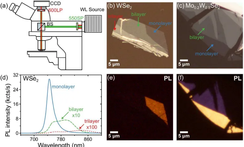
[image:6.612.108.504.178.417.2]Photoluminescence imaging of few-layer TMD samples
Figure 1: Photoluminescence imaging of TMD monolayers and bilayers using a bright-eld optical microscope. (a) Schematic representation of the PL imaging setup based on the optical microscope. (b)-(c) Bright-eld images of mechanically exfoliated few-atomic-layer crystals on PDMS substrates: WSe2 in (b) and Mo0
.2W0.8Se2 in(c). (d) PL
spectra recorded in monolayer (blue), bilayer (green) and trilayer (red) regions of the WSe2
sample shown in (b). (e) PL image of the WSe2 sample acquired with 1 s acquisition time and
9.6x analog gain on the camera, showing PL from the monolayer region only. (f) PL image of the Mo0
.2W0.8Se2 sample shown in (c) with clearly identiable regions of a monolayer
(yellow) and a bilayer (purple). Image recorded with 1 s acquisition time and 3.4x analog gain.
The PL imaging set-up used in this study is schematically shown in Figure 1 (a) and described in more detail in the Methods section below. Figure 1 (b) shows a bright-eld image of a WSe2 ake exfoliated onto a PDMS substrate. The most translucent area in
second acquisition time, the monolayer region is clearly visible in the image due to bright PL emitted by the ake. The PL emission from the WSe2 bilayer region is two orders of
magnitude weaker and requires longer acquisition times to be detected.
The thickness dependence of the PL intensity reects the changes of the WSe2 band
structure with increasing numbers of layers.52 While monolayer WSe2 is a direct bandgap semiconductor, the bandgap becomes indirect for bilayers, leading to a strong quenching of the PL. Figure 1 (d) compares PL spectra recorded in dierent regions of the ake using a separate micro-PL set up (see Methods for details). The monolayer region shows bright PL with emission peak centred at 745 nm (blue line). The direct-to-indirect bandgap transition in bilayer WSe2 leads to a shift of the emission maximum to lower energies, as well as two
orders of magnitude reduction of the emission intensity (dashed green line). Further increase of thickness leads to almost complete disappearance of the PL signal (dotted red line).
The abrupt change of the PL characteristics with increasing numbers of layers allows PL imaging to be used for sample thickness identication. Unlike other methods, such as optical contrast measurements,53 it relies on the change of the TMD band structure and therefore its eectiveness is independent of the type of the substrate used. The exception will be substrates where PL of the TMD monolayers is strongly quenched (for example, when they are placed on gold) or the TMD akes become strongly strained and their band-structure is modied. For such structures our method provides additional insight in the coupling of the ake and substrate and will highlight any non-uniformity of such interaction through the intensity and colour of the PL image.
Figure 1 (c) and (f) compares bright-eld and PL images of a Mo0
.2W0.8Se2 sample
exfoliated onto a PDMS substrate. Compared to the pure binary compound, the TMD alloy shows much brighter PL emission, making both monolayer and bilayer regions clearly visible in the PL image. The dierence in the colour reects the variation of emission spectrum with increasing sample thickness. Similar to WSe2, the PL spectrum broadens
information). PL at longer wavelengths appears as a false purple colour in Fig. 1 (f), a feature related to the transmission eciency in the near-infrared of the colour lter arrays in the digital camera used. The thickness sensitivity of PL imaging makes it a convenient tool for rapid identication of TMD mono- and bilayers on various substrates, including PMMA and PDMS commonly used for vdW heterostructure fabrication (see more image examples in Supplementary information).
Imaging of interlayer coupling in TMD heterobilayers
(d) MoS2
MoSe2
(e)
(c) MoSe2/MoS2
(a) (b) WS2
MoSe2
25 m
25 m
WS2
[image:8.612.107.506.269.521.2]MoSe2
Figure 2: Photoluminescence imaging of CVD-grown TMD samples. (a) Bright-eld image of a MoSe2/WS2 heterostucture on a SiO2/Si substrate. (b) PL image of the
sample in (a) showing that the two materials have distinctly dierent colours according to the wavelength of their PL bands: red for WS2 and a false pink for MoSe2 emitting in
the near infra-red. The PL quenching in the overlap regions indicates ecient electronic coupling between two layers. (c), (d) and (e) Bright-eld, PL, and dark-eld images of a MoSe2/MoS2 heterobilayer on a SiO2/Si substrate. The zoomed-in regions show the same
part of the substrate in all three images, with the PL exhibiting a large amount of additional detail compared to the bright and dark microscopy images. All scale bars in the gure correspond to 25 µm. PL images are recorded with 10 s acquisition time and 9.6x analog gain.
of samples produced by CVD growth, allowing large areas of a sample to be investigated at the same time. Figure 2 (a) show a bright-eld image of a MoSe2/WS2 sample on a SiO2/Si
substrate composed of CVD-grown monolayers. Large triangle in the centre of the image corresponds to single layer WS2 while smaller akes around it are MoSe2 monolayers.
Although both materials have similar appearance in the bright-eld image, they can be easily distinguished by their emission colour in the PL image (Fig. 2 (b)). Room-temperature PL emission of WS2 is centred at 630 nm and appears dark red in the PL image, whereas
MoSe2 PL peaks at 790 nm and has pale pink colour. Here, the MoSe2 monolayers have a
slightly blurry appearance due to the chromatic aberration, as their PL is peaked around 800 nm.
The bright and uniform PL in the WS2 ake indicates high crystalline quality of the
sample. In comparison, the CVD-grown MoS2 akes in a MoSe2/MoS2 sample demonstrate
much weaker PL and signicant variation of the emission intensity both within individual crystals and across the substrate (Fig. 2 (d)). The MoSe2 monolayers in the same sample
also show strongly non-uniform PL emission. The observed 'grainy' structure in PL is likely caused by organic residues left from the transfer process and trapped between the akes or the akes and the substrate. Although the variation of emission intensity within the grainy pattern is clearly visible in the PL image, it shows little correlation with the features visible in the dark-eld image (Fig. 2 (e)) and is completely invisible in the bright-eld image (Fig. 2 (c)).
The overall decrease in the PL intensity is related to the non-radiative decay of electron-hole pairs. The intralayer exciton radiative lifetime is of the order of 1 ps,58,59 while the interlayer excitons radiative decay time exceeds 1 ns.28 The non-radiative processes are ex-tremely fast in TMDs,60 competing with the intralayer exciton radiative decay, so when the excitons are dissociated due to the charge transfer in the heterostructures, the overall PL intensity is signicantly reduced. This process is further enhanced in heterostructures made of misaligned heterobilayers, where the radiative decay of interlayer excitons is sup-pressed due to the momentum mismatch between the electron and hole localised in dierent monolayers.61,62
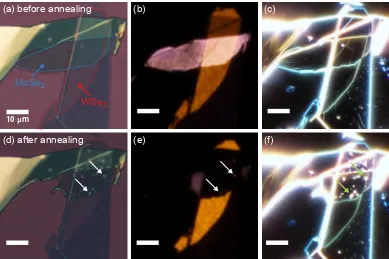
The ecient interlayer coupling in TMD heterostructures requires the interface between adjacent layers to be clean of any contamination. As the van der Waals heterostructure fabrication through mechanical stacking relies on the use of a polymer (PMMA, PC, PDMS etc) as the transfer medium, it often results in the presence of organic residues between the atomic planes. Figure 3 (a) shows an optical image of MoSe2/WSe2 heterostructure
mechanically assembled on a SiO2/Si substrate. The 2D akes exfoliated from bulk crystals
onto a PDMS substrate were consecutively transferred onto the SiO2/Si substrate using
viscoelastic stamping45 with no intermediate cleaning steps. As it can be seen from the PL image in Fig. 3 (b), the PL emitted by the heterobilayer region consists of the sum of MoSe2 and WSe2 emission and shows no signs of PL quenching. The unperturbed intralayer
emission in the heterostructure region indicates that the interlayer coupling is suppressed by the polymer residues trapped between the layers.25,43
Tuning of interlayer coupling through thermal annealing observed in
PL imaging
10 m
(b) (a)
(d) (e)
(c)
(f) after annealing
WSe2 MoSe2
[image:11.612.111.500.71.330.2]before annealing
Figure 3: Monitoring changes in the interlayer coupling introduced by thermal an-nealing. (a), (b), (c) Bright-eld, PL, and dark-eld images of a MoSe2/WSe2
heterostruc-ture fabricated using mechanical exfoliation from bulk crystals on PDMS and consequent transfer on a SiO2/Si substrate. (d), (e), (f) Bright-eld, PL, and dark-eld images of the
same structure after annealing at 120◦ C in high vacuum for 2 hours. Arrows show examples
of contamination pockets observed in all three types of images. All scale bars in the gure correspond to 10 µm. PL images are recorded with 1 s acquisition time and 9.6x analog gain.
images of the sample before (a) and after (d) annealing in high vacuum at 120◦ C for 2 hours.
While a part of the isolated MoSe2 monolayer was damaged during the thermal treatment,
both isolated WSe2 and heterostructure regions remain mostly intact.
heterostruc-tures where the bottom crystal was annealed prior to the deposition of the top ake. The formation of contamination pockets after annealing is similar to the self-cleansing observed in vdW heterostructures4,64and results in atomically clean interfaces in the contamination-free regions.
The eects of the thermal treatment can be clearly seen in the PL image of the sample in Fig. 3 (e). Substantial increase of the emission intensity has occurred in the WSe2
mono-layer,50,65 possibly due to removal of the polymer residues from its surface. The strongest change of the PL intensity can be seen in the layer overlap region, where both MoSe2 and
WSe2 emission has almost completely disappeared after annealing. The strong quenching
of the intralayer PL due to ultrafast charge separation indicates signicant improvement of interlayer coupling.28,34 While the WSe2 emission intensity is signicantly reduced in all areas covered by MoSe2, bright PL can still be observed in the parts of the heterostructure
around the contamination pockets (shown in Fig. 3 (e)). The positions of these bright spots fully correlate with the pockets seen in Fig. 3 (d) and (f)). However, the absence of the electronic coupling in these regions can only be revealed in the PL image in Fig. 3 (e).
Observation of formation of interlayer excitons in TMD
heterobilay-ers using PL imaging
The interlayer charge separation in TMD heterobilayers can lead to the formation of inter-layer excitons formed by electrons and holes localised in dierent materials.2531 The lack of observable emission in the overlap region in Fig. 3 (e) is a result of the combination of the suppression of the interlayer exciton emission in MoSe2/WSe2 at room temperatures and the
which have negligible probability.
(b)
( (e)
(a)
WS2
10 m MoSe
2 WS2 (
(f) MoSe2
Wa e e n)
640 720 800
I(PL ) (kct s/ s) 10 20 30 0 before annealing
after annealing (x5)
[image:13.612.137.476.98.301.2]x30
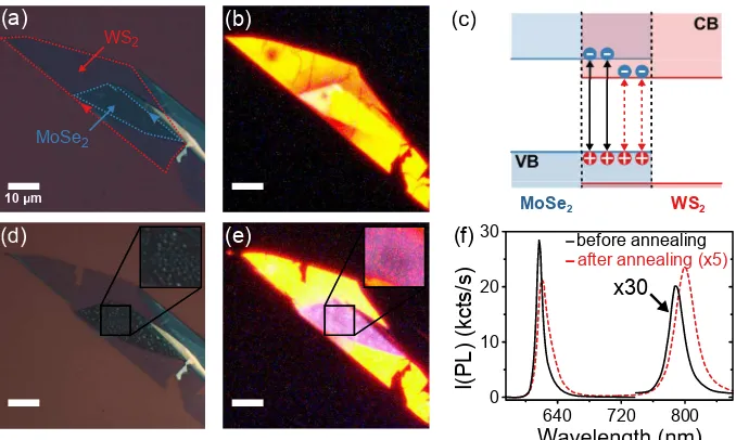
Figure 4: Emergence of interlayer exciton PL following annealing in MoSe2/WS2
heterobilayers. (a) and (b) Bright-eld and PL images of a MoSe2/WS2 heterostructure
fabricated using mechanical exfoliation from bulk crystals on PDMS and consequent transfer on a SiO2/Si substrate. The crystallographic axes of the two monolayers are aligned using the
the ake edges marked with arrows. (c) Band alignment of a MoSe2/WS2 heterostructure
indicating MoSe2 intralayer (solid black) and MoSe2/WS2 interlayer (dashed red) optical
transitions. (d) and (e) Bright-eld and PL images of the sample after annealing. (f) PL spectra of the heterostructure before (solid black) and after (dashed red) annealing. The intensity of the low energy peak in the spectrum measured before the annealing is multiplied by 30, whereas the intensity of the whole spectrum measured after the annealing is multiplied by 5. All scale bars in the gure correspond to 10 µm. PL images are recorded with 10 s acquisition time and 9.6x analog gain.
In order to investigate the eects of annealing on the formation of interlayer excitons in TMD heterobilayers, we have fabricated a set of heterostructures in which crystal axes of mechanically exfoliated akes were aligned using their terminating edges as a guide.66 Figure 4 shows the bright-eld (a) and PL (b) images of a MoSe2/WS2 heterostructure
assembled on a SiO2/Si substrate using PDMS stamping. Both images were taken before
annealing. The PL emission in the overlap region consists mostly of WS2 PL as at room
temperature it is several orders of magnitude stronger than that of MoSe2.30,56
regions of WS2 show an increase of the PL intensity due to removal of the polymer residues,
the heterostructure region demonstrates a prominent change of colour, indicating a signi-cant shift of its peak PL wavelength.
Figure 4 (f) compares the PL spectra of the heterostructure before (solid black) and after (dashed red) annealing. Prior to the thermal treatment, the WS2 PL is nearly two orders
of magnitude stronger than that of MoSe2. Unlike the isolated monolayer regions, WS2
PL in the heterobilayer region is signicantly quenched after annealing due to the ecient interlayer charge separation.30,56 The slight red-shift of the WS
2 peak is possibly a result
of the change in the dielectric environment caused by reduced vertical distance between the layers.29,50,56,67
The emergence of a strong peak at 800 nm following the annealing indicates the forma-tion of interlayer excitons. The emission energy of these excitons is dened by conducforma-tion and valence band osets between the two materials (Fig. 4 (c)). Unlike MoSe2/WSe2
het-erobilayers, the near-degenerate conduction bands in MoSe2/WS2 heterostructure result in
interlayer exciton states having the optical transition just a few tens of meV below the one for MoSe2.30The regions of the heterostructure containing contamination pockets are visible
as spots of a dierent colour in the PL image (magnied in Fig. 4 (e)). The PL in these areas comes from both MoSe2 and WS2, as the aggregated residues prevent ecient coupling
between two materials, causing them to act as independent layers.
Twist angle dependence of the interlayer charge transfer
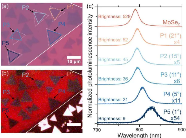
The PL imaging can be directly applied for studying the dependence of the interlayer coupling strength on the relative rotation between the two layers. Figure 5 (a) shows a bright-eld image of the MoSe2/WS2 sample composed of CVD-grown monolayers; dashed white line
marks the edge of a large triangular WS2 monolayer. Since terminating edges of triangular
Figure 5: Twist angle dependence of the interlayer coupling in MoSe2/WS2
heter-obilayers. (a) Bright-eld image of a MoSe2/WS2 heterostructure assembled on a SiO2/Si
substrate from individually CVD-grown layers. Dashed white triangles indicate the orienta-tion of the large triangular WS2 ake, one visible edge of which is marked by a solid white
line. In order to make the relative rotation angles more obvious, the edges of the selected MoSe2 monolayers were highlighted by lines. (b) PL image of the sample showing varying
degrees of the intralayer PL quenching in the overlap regions (see dark triangles); recorded with 10 s acquisition time and 9.6x analog gain. (c) PL spectra measured in the heterobi-layer regions having varying twist angles (shown on the right above each spectrum). The spectra are multiplied by the factors shown on the graph (on the right above each spectrum). The brightness indicated above each curve on the left is extracted from the PL image, as explained in text.
white triangles) with MoSe2 monolayer orientation (coloured triangles). Figure 5 (b) shows
the PL image of the same region. While isolated monolayer regions of both MoSe2 and WS2
the WS2 monolayer and isolated. The average triangle image brightness is calculated as
(R +G+B)/3N, where N is the number of pixels in the triangle, and R, G and B is
the intensity in the red, green and blue channels ranging between 0 and 255. The triangle brightness extracted following this procedure shows that the coherently stacked regions (twist angles of≈0◦) have more than 5 times lower PL intensity compared to rotationally misaligned
areas.
In order to establish rmly the correlation between the PL images and detailed spectral properties of the heterobilayer regions, emission spectra were recorded in the areas with dierent interlayer twist angles using the micro-PL setup. Figure 5 (c) plots normalised PL spectra collected in the regions P1-P5 of the sample, as well as an isolated MoSe2 monolayer.
Scaling factors as well as emission intensity extracted from the PL image are listed above each curve. Compared to the isolated MoSe2 (top curve), the heterobilayer regions demonstrate
red-shifted PL with signicantly lowered intensity, indicating strong interlayer coupling. It is also evident that the PL quenching becomes stronger with the decreasing interlayer twist angle. While the spectral position of the MoSe2 intralayer exciton peak at 795 nm
does not show any clear dependence on the relative orientation of the two layers, for small twist angle the emission peak red-shifts to 830 nm, indicating the change from intralayer to interlayer exciton character. The WS2 PL shows strong quenching in all heterobilayer
regions, however, there is no apparent correlation with the interlayer twist angle (see Fig. S5 in the Supplementary Information).
The angular dependence of the PL intensity can be explained by the relative alignment of the MoSe2 and WS2bands in the momentum space. The edges of the conduction and valence
requires phonon or defect scattering to overcome the in-plane momentum mismatch. As the interlayer twist angle decreases, the K valleys come into alignment, signicantly improving the eciency of charge transfer between two layers. This leads to further quenching of the intralayer exciton PL. In coherently stacked heterobilayers, the band-gap at the Brillouin zone edge becomes direct, leading to the emergence of the interlayer exciton PL.29,31
Conclusions
possible to investigate changes of the interlayer coupling in real time, allowing for example the microscope PL imaging to be used for in-situ monitoring of sample annealing or sur-face functionalisation. With increasing industrial and research interest in devices based on semiconductor vdW heterostructures, the PL imaging developed in this work oers a power-ful characterisation method suitable for both exfoliated and CVD-grown samples at various fabrication stages.
Methods
Optical microscopy system. PL imaging of 2D TMD crystals was carried out using a commercial bright-eld microscope (LV150N, Nikon). The schematic of the experimental setup is presented in Figure 1 (a). A 550 nm short-pass lter (FESH0550, Thorlabs) was used to block the near-infrared emission from the white light source. The PL signal produced by the sample was isolated using 600 nm long-pass lter (FELH0600, Thorlabs). The short-pass (long-short-pass) lters were installed into the polariser (analyser) slots of the illuminator (LV-UEPI-N, Nikon), allowing quick switching between PL and bright-eld imaging modes. The PL images of the samples were acquired using a colour microscope camera (DS-Vi1, Nikon). The hot mirror mounted in front of the sensor was removed in order to enable light detection in the near-infrared range.
Additional micro-PL characterisation. Spectrally resolved PL measurements were performed in a custom-built micro-PL set-up. A diode-pumped solid state laser at 532 nm (CW532-050, Roithner) was focused onto the sample using 50x objective lens (M Plan Apo 50X, Mitutoyo). The PL signal collected in the backwards direction was isolated using a 550 nm shortpass lter (FES0550, Thorlabs) and detected by a spectrometer (SP-2-500i, Princeton Instruments) with a nitrogen cooled CCD camera (PyLoN:100BR, Princeton In-struments). All spectrally resolved PL measurements were performed at room temperature and in ambient conditions.
exfo-liated from bulk crystals (provided by HQ Graphene) using wafer backgrinding tape (BT-150E-CM, Nitto). Van der Waals heterostructures were fabricated by exfoliating material onto a PDMS membrane (PF X4, Gel-Pak) followed by a transfer onto SiO2/Si using a
viscoelastic stamping method.
CVD WS2 and MoS2 crystals were grown directly on a SiO2/Si substrate with a 300 nm
thick SiO2 layer. For heterostructure fabrication, MoSe2 monolayers grown on c-plane
sap-phire substrates were transferred onto the substrate containing WS2 and MoS2 akes using
PMMA-assisted transfer - see the Supplementary Information for more details.
Supporting Information Available
Optical identication of TMD monolayers and bilayers on various substrates; selective imag-ing of dierent materials in a van der Waals heterostructure; PL spectra for mono-, bi- and trilayer Mo0
.2W0.8Se2; low-temperature PL spectrum of the MoSe2/WS2 heterostructure
be-fore and after annealing; interlayer twist angle dependence of WS2 emission in a MoSe2/WS2
heterostructures; information on the growth of the CVD MoS2, MoSe2 and WS2 monolayers
and fabrication of heterobilayers.
Acknowledgement
The authors thank the nancial support of the EPSRC grant EP/M012727/1, Graphene Flagship under grant agreement 696656, and ITN Spin-NANO under grant agreement 676108.
References
(1) Li, M. Y.; Chen, C. H.; Shi, Y.; Li, L. J. Mater. Today 2015, 19, 322335.
(3) Liu, Y.; Weiss, N. O.; Duan, X.; Cheng, H.-C.; Huang, Y.; Xiangfeng, D. Nat. Rev. Mater. 2016, 1, 16042.
(4) Novoselov, K. S.; Mishchenko, A.; Carvalho, A.; Neto, A. H. C.; Road, O. Science 2016, 353, aac9439.
(5) Roy, T.; Tosun, M.; Kang, J. S.; Sachid, A. B.; Desai, S. B.; Hettick, M.; Hu, C. C.; Javey, A. ACS Nano 2014, 8, 62596264.
(6) Das, S.; Gulotty, R.; Sumant, A. V.; Roelofs, A. Nano Lett. 2014, 14, 28612866.
(7) Lee, G.-h.; Cui, X.; Kim, D.; Arefe, G.; Zhang, X.; Lee, C.-h.; Ye, F.; Wantanabe, K.; Taniguchi, T.; Hone, J. ACS Nano 2015, 9, 70197026.
(8) Liu, Y.; Wu, H.; Cheng, H.-C. C.; Yang, S.; Zhu, E.; He, Q.; Ding, M.; Li, D.; Guo, J.; Weiss, N. O.; Huang, Y.; Duan, X. Nano Lett. 2015, 15, 30303034.
(9) Cui, X.; Lee, G.-H.; Kim, Y. D.; Arefe, G.; Huang, P. Y.; Lee, C.-H.; Chenet, D. A.; Zhang, X.; Wang, L.; Ye, F. et al. Nat. Nanotechnol. 2015, 10, 534540.
(10) Ross, J. S.; Klement, P.; Jones, A. M.; Ghimire, N. J.; Yan, J.; Mandrus, D. G.; Taniguchi, T.; Watanabe, K.; Kitamura, K.; Yao, W.; Cobden, D. H.; Xu, X. Nat. Nanotechnol. 2014, 9, 268272.
(11) Cheng, R.; Li, D.; Zhou, H.; Wang, C.; Yin, A.; Jiang, S.; Liu, Y.; Chen, Y.; Huang, Y.; Duan, X. Nano Lett. 2014, 14, 55905597.
(12) Withers, F.; Del Pozo-Zamudio, O.; Schwarz, S.; Duerwiel, S.; Walker, P. M.; Godde, T.; Rooney, A. P.; Gholinia, A.; Woods, C. R.; Blake, P. et al. Nano Lett. 2015, 15, 82238228.
(14) Britnell, L.; Gorbachev, R. V.; Jalil, R.; Belle, B. D.; Schedin, F.; Mishchenko, A.; Georgiou, T.; Katsnelson, M. I.; Eaves, L.; Morozov, S. V.; Peres, N. M. R.; Leist, J.; Geim, A. K.; Novoselov, K. S.; Ponomarenko, L. A. Science 2012, 335, 947950.
(15) Britnell, L.; Gorbachev, R. V.; Geim, A. K.; Ponomarenko, L. A.; Mishchenko, A.; Greenaway, M. T.; Fromhold, T. M.; Novoselov, K. S.; Eaves, L. Nat. Commun. 2013, 4, 1794.
(16) Lin, Y.-C.; Ghosh, R. K.; Addou, R.; Lu, N.; Eichfeld, S. M.; Zhu, H.; Li, M.-Y.; Peng, X.; Kim, M. J.; Li, L.-J.; Wallace, R. M.; Datta, S.; Robinson, J. A. Nat. Commun. 2015, 6, 7311.
(17) Roy, T.; Tosun, M.; Cao, X.; Fang, H.; Lien, D.-H.; Zhao, P.; Chen, Y.-Z.; Chueh, Y.-L.; Guo, J.; Javey, A. ACS Nano 2015, 9, 20712079.
(18) Buscema, M.; Island, J. O.; Groenendijk, D. J.; Blanter, S. I.; Steele, G. A.; van der Zant, H. S.; Castellanos-Gomez, A. Chem. Soc. Rev. 2015, 44, 36913718.
(19) Buscema, M.; Groenendijk, D. J.; Steele, G. a.; van der Zant, H. S. J.; Castellanos-Gomez, A. Nat. Commun. 2014, 5, 4651.
(20) Furchi, M. M.; Pospischil, A.; Libisch, F.; Burgdörfer, J.; Mueller, T.; Burgdo, J.; Mueller, T. Nano Lett. 2014, 14, 47854791.
(21) Lee, C.-H.; Lee, G.-H.; van der Zande, A. M.; Chen, W.; Li, Y.; Han, M.; Cui, X.; Arefe, G.; Nuckolls, C.; Heinz, T. F.; Guo, J.; Hone, J.; Kim, P. Nat. Nanotechnol. 2014, 9, 676681.
(22) Lou, J.; Xu, X.; Ye, P. D. ACS Nano 2014, 8, 82928299.
(24) Yu, W. J.; Vu, Q. A.; Oh, H.; Nam, H. G.; Zhou, H.; Cha, S.; Kim, J.-Y.; Carvalho, A.; Jeong, M.; Choi, H.; Castro Neto, A. H.; Lee, Y. H.; Duan, X. Nat. Commun. 2016, 7, 13278.
(25) Tongay, S.; Fan, W.; Kang, J.; Park, J.; Koldemir, U.; Suh, J.; Narang, D. S.; Liu, K.; Ji, J.; Li, J.; Sinclair, R.; Wu, J. Nano Lett. 2014, 14, 31853190.
(26) Fang, H.; Battaglia, C.; Carraro, C.; Nemsak, S.; Ozdol, B.; Kang, J. S.; Bechtel, H. a; Desai, S. B.; Kronast, F.; Unal, A. A et al. Proc. Natl. Acad. Sci. U. S. A. 2014, 111, 61986202.
(27) Lui, C. H.; Ye, Z.; Ji, C.; Chiu, K. C.; Chou, C. T.; Andersen, T. I.; Means-Shively, C.; Anderson, H.; Wu, J. M.; Kidd, T.; Lee, Y. H.; He, R. Phys. Rev. B 2015, 91, 165403.
(28) Rivera, P.; Schaibley, J. R.; Jones, A. M.; Ross, J. S.; Wu, S.; Aivazian, G.; Klement, P.; Seyler, K.; Clark, G.; Ghimire, N. J.; Yan, J.; Mandrus, D. G.; Yao, W.; Xu, X. Nat. Commun. 2015, 6, 6242.
(29) Heo, H.; Sung, J. H.; Cha, S.; Jang, B.-G.; Kim, J.-Y.; Jin, G.; Lee, D.; Ahn, J.-H.; Lee, M.-J.; Shim, J. H.; Choi, H.; Jo, M.-H. Nat. Commun. 2015, 6, 7372.
(30) Ceballos, F.; Bellus, M. Z.; Chiu, H.-Y.; Zhao, H. Nanoscale 2015, 7, 1752317528.
(31) Nayak, P. K.; Horbatenko, Y.; Ahn, S.; Kim, G.; Lee, J.-U.; Ma, K. Y.; Jang, A.-R.; Lim, H.; Kim, D.; Ryu, S.; Cheong, H.; Park, N.; Shin, H. S. ACS Nano 2017, 11, 40414050.
(32) Wilson, N. R.; Nguyen, P. V.; Seyler, K. L.; Rivera, P.; Marsden, A. J.; Laker, Z. P. L.; Constantinescu, G. C.; Kandyba, V.; Barinov, A.; Hine, N. D. M.; Xu, X.; Cobden, D. H. arXiv preprint arXiv:1601.05865, 2016.
(34) Rivera, P.; Seyler, K.; Yu, H.; Schaibley, J.; Yan, J.; Mandrus, D.; Yao, W.; Xu, X. Science 2016, 351, 688.
(35) Huang, C.; Wu, S.; Sanchez, A. M.; Peters, J. J. P.; Beanland, R.; Ross, J. S.; Rivera, P.; Yao, W.; Cobden, D. H.; Xu, X. Nat. Mater. 2014, 13, 10961101.
(36) Duan, X.; Wang, C.; Shaw, J. C.; Cheng, R.; Chen, Y.; Li, H.; Wu, X.; Tang, Y.; Zhang, Q.; Pan, A.; Jiang, J.; Yu, R.; Huang, Y.; Duan, X. Nat. Nanotechnol. 2014, 9, 10241030.
(37) Gong, Y.; Lei, S.; Ye, G.; Li, B.; He, Y.; Keyshar, K.; Zhang, X.; Wang, Q.; Lou, J.; Liu, Z.; Vajtai, R.; Zhou, W.; Ajayan, P. M. Nano Lett. 2015, 15, 61356141.
(38) Yoshida, S.; Kobayashi, Y.; Sakurada, R.; Mori, S.; Miyata, Y.; Mogi, H.; Koyama, T.; Takeuchi, O.; Shigekawa, H. Sci. Rep. 2015, 5, 14808.
(39) Li, H.; Zhang, Q.; Duan, X.; Wu, X.; Fan, X.; Zhu, X.; Zhuang, X.; Hu, W.; Zhou, H.; Pan, A.; Duan, X. J. Am. Chem. Soc. 2015, 137, 52845287.
(40) Li, M.-Y.; Shi, Y.; Cheng, C.; Lu, L.-S.; Lin, Y.-C.; Tang, H.-L.; Tsai, M.-L.; Chu, C.-W.; Wei, K.-H.; He, J.-H.; Chang, W.-H.; Suenaga, K.; Li, L.-J. Science 2015, 349, 524528.
(41) Pant, A.; Mutlu, Z.; Wickramaratne, D.; Cai, H.; Lake, R. K.; Ozkan, C.; Tongay, S. Nanoscale 2016, 8, 38703887.
(42) Gong, Y.; Lin, J.; Wang, X.; Shi, G.; Lei, S.; Lin, Z.; Zou, X.; Ye, G.; Vajtai, R.; Yakobson, B. I. et al. Nat. Mater. 2014, 13, 11351142.
(43) Yu, Y.; Hu, S.; Su, L.; Huang, L.; Liu, Y.; Jin, Z.; Purezky, A. A.; Geohegan, D. B.; Kim, K. W.; Zhang, Y.; Cao, L. Nano Lett. 2015, 15, 486491.
(45) Castellanos-Gomez, A.; Buscema, M.; Molenaar, R.; Singh, V.; Janssen, L.; van der Zant, H. S. J.; Steele, G. a. 2D Mater. 2014, 1, 011002.
(46) Uwanno, T.; Hattori, Y.; Taniguchi, T.; Watanabe, K.; Nagashio, K. 2D Mater. 2015, 2, 041002.
(47) Chiu, M. H.; Li, M. Y.; Zhang, W.; Hsu, W. T.; Chang, W. H.; Terrones, M.; Ter-rones, H.; Li, L. J. ACS Nano 2014, 8, 96499656.
(48) Hong, X.; Kim, J.; Shi, S.-F.; Zhang, Y.; Jin, C.; Sun, Y.; Tongay, S.; Wu, J.; Zhang, Y.; Wang, F. Nat. Nanotechnol. 2014, 9, 682686.
(49) Zhang, K.; Zhang, T.; Cheng, G.; Li, T.; Wang, S.; Wei, W.; Zhou, X.; Yu, W.; Sun, Y.; Wang, P. et al. ACS Nano 2016, 10, 38523858.
(50) Wang, K.; Huang, B.; Tian, M.; Ceballos, F.; Lin, M.-W.; Mahjouri-Samani, M.; Boulesbaa, A.; Puretzky, A. A.; Rouleau, C. M.; Yoon, M.; Zhao, H.; Xiao, K.; Duscher, G.; Geohegan, D. B. ACS Nano 2016, 10, 66126622.
(51) Xu, W.; Liu, W.; Schmidt, J. F.; Zhao, W.; Lu, X.; Raab, T.; Diederichs, C.; Gao, W.; Seletskiy, D. V.; Xiong, Q. Nature 2016, 541, 6267.
(52) Tonndorf, P.; Schmidt, R.; Böttger, P.; Zhang, X.; Börner, J.; Liebig, A.; Albrecht, M.; Kloc, C.; Gordan, O.; Zahn, D. R. T.; Michaelis de Vasconcellos, S.; Bratschitsch, R. Opt. Express 2013, 21, 4908.
(53) Casiraghi, C.; Hartschuh, A.; Lidorikis, E.; Qian, H.; Harutyunyan, H.; Gokus, T.; Novoselov, K. S.; Ferrari, A. C. Nano Lett. 2007, 7, 27112717.
(54) Kang, J.; Tongay, S.; Zhou, J.; Li, J.; Wu, J. Appl. Phys. Lett. 2013, 102, 012111.
(56) Kozawa, D.; Carvalho, A.; Verzhbitskiy, I.; Giustiniano, F.; Miyauchi, Y.; Mouri, S.; Neto, A. H. C.; Matsuda, K.; Eda, G. Nano Lett. 2016, 16, 40874093.
(57) Ceballos, F.; Bellus, M. Z.; Chiu, H.-Y.; Zhao, H. ACS Nano 2014, 8, 1271712724.
(58) Robert, C.; Lagarde, D.; Cadiz, F.; Wang, G.; Lassagne, B.; Amand, T.; Balocchi, A.; Renucci, P.; Tongay, S.; Urbaszek, B.; Marie, X. Phys. Rev. B 2016, 93, 205423.
(59) Duerwiel, S.; Schwarz, S.; Withers, F.; Trichet, A. A. P.; Li, F.; Sich, M.; Del Pozo-Zamudio, O.; Clark, C.; Nalitov, A.; Solnyshkov, D. D. et al. Nat. Commun. 2015, 6, 8579.
(60) Mak, K. F.; Lee, C.; Hone, J.; Shan, J.; Heinz, T. F. Phys. Rev. Lett. 2010, 105, 136805.
(61) Yu, H.; Wang, Y.; Tong, Q.; Xu, X.; Yao, W. Phys. Rev. Lett. 2015, 115, 187002.
(62) Wang, Y.; Wang, Z.; Yao, W.; Liu, G.-B.; Yu, H. 3941. Phys. Rev. B 2017, 95, 3941.
(63) Vasu, K. S.; Prestat, E.; Abraham, J.; Dix, J.; Kashtiban, R. J.; Beheshtian, J.; Sloan, J. Nat. Commun. 2016, 7, 124.
(64) Kretinin, A. V.; Cao, Y.; Tu, J. S.; Yu, G. L.; Jalil, R.; Novoselov, K. S.; Haigh, S. J.; Gholinia, A.; Mishchenko, A.; Lozada, M. et al. Nano Lett. 2014, 14, 32703276.
(65) Su, L.; Yu, Y.; Cao, L.; Zhang, Y. arXiv preprint arXiv:1609.05077, 2016.
(66) Neubeck, S.; You, Y. M.; Ni, Z. H.; Blake, P.; Shen, Z. X.; Geim, A. K.; Novoselov, K. S. Appl. Phys. Lett. 2010, 97, 20102012.
(67) Kim, M. S.; Seo, C.; Kim, H.; Lee, J.; Luong, D. H.; Park, J. H.; Han, G. H.; Kim, J. ACS Nano 2016, 10, 62116219.
Graphical TOC Entry
25 m
W 2
M 2
W2