This content has been downloaded from IOPscience. Please scroll down to see the full text.
Download details:
IP Address: 129.11.22.210
This content was downloaded on 04/01/2017 at 15:03
Please note that terms and conditions apply.
The 2017 terahertz science and technology roadmap
View the table of contents for this issue, or go to the journal homepage for more 2017 J. Phys. D: Appl. Phys. 50 043001
(http://iopscience.iop.org/0022-3727/50/4/043001)
1 © 2017 IOP Publishing Ltd Printed in the UK Journal of Physics D: Applied Physics
S S Dhillon et al
Printed in the UK
043001 JPAPBE
© 2017 IOP Publishing Ltd 50
J. Phys. D: Appl. Phys.
JPD
10.1088/1361-6463/50/4/043001
4
Journal of Physics D: Applied Physics
The 2017 terahertz science and technology
roadmap
S S Dhillon1, M S Vitiello2, E H Linfield3, A G Davies3,
Matthias C Hoffmann4, John Booske5, Claudio Paoloni6, M Gensch7, P Weightman8, G P Williams9, E Castro-Camus10, D R S Cumming11, F Simoens12, I Escorcia-Carranza11, J Grant11, Stepan Lucyszyn13, Makoto Kuwata-Gonokami14, Kuniaki Konishi14, Martin Koch15, Charles A Schmuttenmaer16, Tyler L Cocker17, Rupert Huber17, A G Markelz18, Z D Taylor19, Vincent P Wallace20, J Axel Zeitler21, Juraj Sibik21, Timothy M Korter22, B Ellison23, S Rea23, P Goldsmith24, Ken B Cooper25, Roger Appleby26, D Pardo23, P G Huggard23, V Krozer27, Haymen Shams28, Martyn Fice28, Cyril Renaud28, Alwyn Seeds28,
Andreas Stöhr29, Mira Naftaly30, Nick Ridler30, Roland Clarke31, John E Cunningham3,33 and Michael B Johnston32,33
1 Laboratoire Pierre Aigrain, Ecole Normale Supérieure-PSL Research University, CNRS, Université Pierre et Marie Curie-Sorbonne Universités, Université Paris Diderot-Sorbonne Paris Cité, 75231 Paris, France
2 NEST, CNR—Istituto Nanoscienze and Scuola Normale Superiore, Piazza San Silvestro 12, 56127 Pisa, Italy
3 School of Electronic and Electrical Engineering, University of Leeds, Leeds, LS2 9JT, UK
4 Linac Coherent Light Source, SLAC National Accelerator Laboratory, Menlo Park, CA 94025, USA 5 Electrical and Computer Engineering Department, University of Wisconsin - Madison, USA 6 Engineering Department, Lancaster University, Lancaster, UK
7 Helmholtz-Zentrum Dresden-Rossendorf, Institute of Radiation Physics, Bautzner Landstr. 400, 01328 Dresden, Germany
8 Physics Department, University of Liverpool, Liverpool, L69 7ZE, UK
9 Jefferson Laboratory, 12000 Jefferson Avenue—Suite 21 Newport News, VA 23606, USA 10 Centro de Investigaciones en Optica A.C., Loma del Bosque 115, Lomas del Campestre, Leon, Guanajuato 37150, Mexico
11 Microsystems Technology Group, School of Engineering, University of Glasgow, Glasgow, G12 8LT, UK 12 CEA-Leti MINATEC, 17 rue des Martyrs, Grenoble, Cedex 9 38054, France
13 Department of EEE, Centre for Terahertz Science and Engineering, Imperial College London, London, UK
14 Department of Physics, University of Tokyo, Tokyo, Japan
15 Faculty of Physics and Material Sciences Center, Philipps-Universität Marburg, Marburg D-35032, Germany
16 Department of Chemistry and Energy Sciences Institute, Yale University, 225 Prospect Street, P.O. Box 208107, New Haven, Connecticut 06520-8107, USA
17 Institut für Experimentelle und Angewandte Physik, Universität Regensburg, Universitätsstraße 31, 93053 Regensburg, Germany
18 Department of Physics, University at Buffalo, The State University of New York, Buffalo, NY 14620, USA
19 Department of Bioengineering, University of California, Los Angeles, CA 90095, USA
Topical Review
IOP
Original content from this work may be used under the terms of the Creative Commons Attribution 3.0 licence. Any further distribution of this work must maintain attribution to the author(s) and the title of the work, journal citation and DOI.
33 All correspondence should be addressed to the editors of this Roadmap
article: Michael Johnston ([email protected]) and John Cunningham ([email protected]).
2017
1361-6463
1361-6463/17/043001+49$33.00
20 The University of Western Australia (M013), 35 Stirling Highway, CRAWLEY WA 6009, Australia 21 Department of Chemical Engineering, Magnetic Resonance Research Centre, JJ Thompson Avenue, Cambridge, CB3 0HE, UK
22 Syracuse University, Department of Chemistry, 1-014 CST, 111 College Place, Syracuse, NY 13244-4100, USA
23 Millimetre Wave Technology Group, STFC, RAL Space, OX11 0QX, UK
24 Jet Propulsion Laboratory, M/S 180-703, 4800 Oak Grove Drive, Pasadena, CA 91109, USA 25 Jet Propulsion Laboratory, California Institute of Technology, Pasadena, CA, USA
26 Innovasec Ltd, 212b West Malvern Road, Malvern, Worcs, WR14 4BA, UK
27 Goethe-Leibniz Terahertz Center, Goethe University of Frankfurt am Main, 60323 Frankfurt am Main, Germany
28 Department of Electronic and Electrical Engineering, University College London, Torrington Place, London, WC1E 7JE, UK
29 Department of Optoelectronics, Faculty of Engineering, University of Duisburg-Essen, Lotharstr. 55, 47057 Duisburg, Germany
30 Division of Time, Quantum and Electromagnetics, National Physical Laboratory, Teddington, TW11 0LW, UK
31 School of Electronic and Electrical Engineering, University of Leeds, Leeds, LS2 9JT, UK
32 Department of Physics, University of Oxford, Clarendon Laboratory, Parks Road, Oxford OX1 3PU, UK
E-mail: [email protected] and [email protected]
Received 9 May 2016, revised 29 September 2016 Accepted for publication 12 October 2016 Published 4 January 2017
Abstract
Science and technologies based on terahertz frequency electromagnetic radiation (100 GHz–30 THz) have developed rapidly over the last 30 years. For most of the 20th Century, terahertz radiation, then referred to as sub-millimeter wave or far-infrared radiation, was mainly utilized by astronomers and some spectroscopists. Following the development of laser based terahertz time-domain spectroscopy in the 1980s and 1990s the field of THz science and technology expanded rapidly, to the extent that it now touches many areas from fundamental science to ‘real world’ applications. For example THz radiation is being used to optimize materials for new solar cells, and may also be a key technology for the next generation of airport security scanners. While the field was emerging it was possible to keep track of all new developments, however now the field has grown so much that it is increasingly difficult to follow the diverse range of new discoveries and applications that are appearing. At this point in time, when the field of THz science and technology is moving from an emerging to a more established and interdisciplinary field, it is apt to present a roadmap to help identify the breadth and future directions of the field. The aim of this roadmap is to present a snapshot of the present state of THz science and technology in 2017, and provide an opinion on the challenges and opportunities that the future holds. To be able to achieve this aim, we have invited a group of international experts to write 18 sections that cover most of the key areas of THz science and technology. We hope that The 2017 Roadmap on THz science and technology will prove to be a useful resource by providing a wide ranging introduction to the capabilities of THz radiation for those outside or just entering the field as well as providing perspective and breadth for those who are well established. We also feel that this review should serve as a useful guide for government and funding agencies.
Keywords: terahertz, time-domain spectroscopy, semiconductors
3 Contents
1. Terahertz quantum cascade lasers 4
2. Intense laser-based THz sources 6
3. THz vacuum electronics 8
4. Accelerator-based sources of terahertz radiation 10
5. Photoconductive devices for THz time-domain spectroscopy 12
6. Components for terahertz imaging 14
7. Passive THz components 18
8. Developments in THz time domain spectroscopy 21
9. Terahertz spectroscopy of semiconductors and semiconductor nanostructures 23
10. THz microscopy 26
11. Biological applications of THz technology 28
12. Medical applications 30
13. Non-destructive testing and molecular spectroscopy 32
14. THz technology—the rocket road to space 35
15. Terahertz components and systems for defence and security imaging 37
16. Semiconductor device based THz detection 39
17. Status of THz communications 41
1. Terahertz quantum cascade lasers
S S Dhillon1, M S Vitiello2, E H Linfield3 and A G Davies3
1 Laboratoire Pierre Aigrain, Ecole Normale Supérieure-PSL Research University, CNRS, Université Pierre et Marie Curie-Sorbonne Universités, Université Paris Diderot-Sorbonne Paris Cité, 75231 Paris, France.
2 NEST, CNR—Istituto Nanoscienze and Scuola Normale Superiore, Piazza San Silvestro 12, 56127 Pisa, Italy
3 School of Electronic and Electrical Engineering, University of Leeds, Leeds, LS2 9JT, UK
Status. Quantum cascade lasers (QCLs) are compact semi-conductor sources exploiting III–V superlattice materials that were first demonstrated in the mid-infrared (mid-IR) and, since 2002, in the THz frequency range [1]. Laser action arises from transitions between electronic subbands formed in a series of quantum wells and, by ‘cascading’ a number of such active regions together, the injected electrons undergo multiple las-ing transitions as they pass through the device (see figure 1a). The entire characteristics of the laser can therefore be con-trolled through bandstructure engineering and by the design of the semiconductor superlattice. The QCL concept has enabled powerful and compact sources to be realized in previ-ously inaccessible regions of the electromagnetic spectrum. In the mid-IR, QCLs have achieved impressive performance levels with multi-Watt output power, room temperature (RT) and continuous wave (CW) operation with wall-plug efficien-cies of up to 21% at RT, and can cover a wide spectral range of 2.7–25 µm. Beyond the Restrahlen band (>50 µm), QCLs have also shown remarkable performances over the range 1–5 THz range, with demonstration of high powers (>1 W), photonic and far-field engineering, a quantum limited line-width, frequency combs and pulse generation [2]. These advances have permitted THz QCLs to be made commercially available and, although cryogenic cooling is still required, this can be achieved conveniently and inexpensively with Stirling coolers. A wide range of applications are now being targeted from local oscillators for astronomy, to use in metrology and non-destructive imaging [2]. Although there remain chal-lenges, the further development and exploitation of THz QCLs is crucial owing to the unparalleled success of these devices in terms of their output power and wavelength agility in a com-pact, potentially inexpensive and user-friendly geometry.
Current and future challenges. After a decade of research, the operation temperature of THz QCLs has progressively risen to 199.5 K in pulsed mode [3] (and in the absence of an applied magnetic field), although this maximum temper-ature has stayed static now for a number of years. The GaAs/ AlGaAs material system and active region designs are likely to be the limiting factors. Although commercial systems exploit-ing such QCLs can be based around Stirlexploit-ing coolers, for more mainstream applications and lower cost, Peltier cooling would be beneficial. However, this will require an increase in the cur-rent maximum operating temperature to around 240 K.
An alternative methodology is to leverage advances in high-power two-colour mid-IR QCLs for room temperature,
intra-cavity THz difference frequency generation [4]. Although the emission is not as powerful as from THz QCLs, this route has shown intriguing breakthroughs in temperature operation and tunability. A challenge here is to overcome the wall-plug efficiency limit, which is at best just ~10−6.
Two types of THz QCL waveguides are implemented: the surface plasmon (single metal) waveguide, and the metal– metal (MM) waveguide (Figure 1b). The latter is beneficial for higher temperature operation, and for lower QCL fre-quency operation, although at the cost of a poorer output beam profile and lower output power. Initial efforts to address this employed facet-mounted lenses, horn-antennas and photonic crystals. Nonetheless, these do not simultaneously satisfy the requirements of monolithic geometry, high power and a controlled far-field radiation profile. Photonic heterostruc-tured and 3rd order DFB geometries currently provide poten-tially valuable solutions to address this challenge [5]. These approaches, however, are all frequency-selective in nature, and are therefore not appropriate for broadband coupling that would be required for future challenges such as broadband amplifiers, pulse generation and frequency combs (see below). Broadband, efficient integrated couplers for THz QCLs there-fore represent an important future goal, particularly operating at very high powers.
Tuning of the QCL frequency emission is also an impor-tant challenge. Although the spectral linewidth of the QCL [6] is ideal for gas spectroscopy, tuning remains non-ideal. Although a range of solutions have been realized including through temperature control, multi-section DFB structures [7], and Vernier tuning [8], the tuning range is proving to be limited. An important step would be the realization of an external cavity with a THz QCL gain medium. For this, effi-cient anti-reflection coatings that can cover a large spectral range need to be developed.
The investigation of schemes for developing broadband THz QCL frequency combs (FCs), is a topic of consider-able current interest [9, 10] where the compensation of the index dispersion over a large frequency range is vital. Complementary to this is short pulse generation from QCLs, where currently 10 ps pulses can be generated at best, with relatively low output powers [11, 12]. This is a direct conse-quence of the ultrafast QCL dynamics. Future development will be needed to meet the challenge of simultaneous genera-tion of much shorter pulses with high powers through new modelocking geometries.
An important challenge will be to bring these develop-ments in source technology towards systems, requiring new approaches to THz detection in terms of rapidity and sen-sitivity at high temperatures. Promising directions include self-mixing, down- and up-conversion, and nano-detection technologies (QWIPs, nanowires or quantum-dot approaches). This will work towards complete THz systems, promising breakthroughs in optical communication, quantum comput-ing, dual-comb spectroscopy and time-of-flight tomography.
5 materials system, other semiconductor materials such as InGaAs and InAs have gained attention, not least owing to their lower effective masses and therefore higher gain. High quality growth with control of the optical losses is vital here, however. More exotic systems currently being explored include SiGe heterostructures, III-nitride quantum wells and even II–VI systems. The latter two materials have large LO phonon energies (>70 meV) and so the major bottleneck for high-temperature operation (thermally activated LO-phonon scattering) should be dramatically suppressed. An even more radical approach to suppress non-radiative scattering is to implement a cascade laser within a series of quantum-dots, rather than through quantum-wells. This would potentially result in zero energy dispersion in momentum space, thus reducing non-radiative scattering [13]. Both top-down and bottom-up investigations of quantum-dot patterning are being made or have been proposed, with the former dependent on improvements in advanced processing techniques and surface passivation, and the latter requiring new growth techniques such as in situ site-controlled dots.
In the context of room temperature intracavity THz differ-ence frequency generation, this would benefit from advances in mid-IR QCLs with a shift towards shorter mid-IR wave-lengths (~5 µm) that show better wall-plug efficiency that will directly improve the THz output power. Although the current geometry relies on the Cherenkov coupling scheme, and is efficient in extracting the THz radiation, the use of both passive waveguides and more traditional phase matching schemes may allow the realization of an electrically pumped chip-based THz optical parametric oscillator.
To address the ambition for integrated spectrometers and broadly tunable sensing systems, different technological solu-tions can be envisioned: arrays of vertical-emitting ring-cav-ities or distributed feedback lasers in master-oscillator power amplifier configurations [14], and heterogeneous QCLs in
external cavity systems, represent, respectively, very prom-ising solutions. A possible option for broadband, efficient integrated THz out-couplers could be the exploitation of quasi-periodic structures (1D gratings, 2D quasi-crystals) or even random resonators to break the symmetry of the radiat-ing modes [15]. In terms of THz QCL tunability, extremely narrow double-metal cavities combined with refined MEMS systems [16] or surface-emitting resonators in coupled micro-cavity architectures, exploiting metallic mirrors, graphene or metamaterials have potential. Finally, to address the devel-opment of a broadband QCL FC, group velocity dispersion can be significantly reduced through new active regions, waveguide designs, and integrated chirped mirrors. Short pulse generation via mode-locking [17] can also take advan-tage of these advances and by implementing hybrid active-passive approaches or by devising suitable saturable absorber comp onents with novel architectures, or by exploiting novel, still unexplored materials, with appropriate THz absorption features.
Concluding remarks. Although there remain considerable challenges ahead, THz frequency QCLs are currently the only compact source operating with high output powers above 1 THz. Through the potential advances highlighted above, fur-ther applications and functionalities of these devices will be found ranging from fundamental science to applied research, including their use as new sources for nonlinear optics, imag-ing, spectroscopy and trace gas analysis, inter alia. There remain open questions on the operation of these devices, including their high temperature performance, their dynam-ics related to pulse generation, and the possibility to realize extremely broadband frequency combs. Further, QCLs will accompany new advances in detector technology, such as coherent detection and nano-detection techniques, to provide powerful, inexpensive and compact THz systems.
2. Intense laser-based THz sources
Matthias C Hoffmann
Linac Coherent Light Source, SLAC National Accelerator Laboratory, Menlo Park, CA 94025
Status. The spectral range between 0.3 and 30 THz has long been described as the ‘THz gap’ because of the lack of strong and compact sources. This has changed drastically in the last two decades. CW-sources based on microwave tech-nology (see summary in section 6) and solid state sources based on quantum cascade laser technology (see section 1) are now available and offer average power in the mW range. Dramatic improvements have also been made in the genera-tion of intense picosecond THz pulses via nonlinear optical methods such as optical rectification [25]. It is now possible to routinely generate pulse energies of tens of micro-joules and field strengths exceeding 1 MV cm−1 with a compact and reli-able femtosecond laser source in a small university laboratory without issues of restricted access, low repetition rate, timing stability and beam transport issues in accelerator-based THz facilities.
The most promising applications of these strong-field THz sources are in basic science. Here, researchers take advantage of the fact that resonant excitation in the THz and far-infrared range can be used to selectively deposit energy into specific low frequency modes of the material. This is of great impor-tance to study non-equilibrium dynamics of complex matter such as unconventional superconductors, multiferroics and magnetic materials [18] and semiconductors (see section 9). Femtosecond laser pulses typically have wavelengths in the visible or near-infrared range, and have photon energies in the range of 1–2 eV, well above the band gap energy of many complex materials. Pumping materials directly at these pho-ton energies result in a cascade of photo-induced processes that can obscure the more subtle low energy phenomena. Various optical, THz or ultrafast x-ray probe techniques can then be used to study the response of the system. New ways of understanding collective phenomena are possible when the coupling between electronic, spin and vibrational degrees of freedom is untangled. This has been demonstrated success-fully in several mid-infrared pump experiments, where direct control over a structural phonon is exerted by the laser [19].
A further avenue to control complex materials is to take advantage of the high peak magnetic fields present in a THz pulse which can approach 1 T, enabling ultrafast control of magnetism.
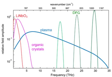
Current and future challenges. A schematic overview of currently available THz sources is shown in figure 2. Pres-ent laser-based sources are able to produce single-cycle pulses centred at 1 THz or quasi-single cycle centred at 2 THz with peak fields on the order of 1 or 2 MV cm−1. The two main techniques are optical rectification in LiNbO3 with tilted pulse front (TPF) pumping [21] or optical rectification in organic crystals with an extremely high nonlinear constant χ(2). The TPF technique can be deployed with various pump wave-lengths and powerful Ti:Sapphire or Yb:YAG lasers can be
used at their fundamental wavelengths to drive the rectifica-tion process. Scaling to high average power/high repetirectifica-tion rate is also possible. The spectral content of the resulting THz pulses is limited to <3 THz by material absorption. Organic nonlinear crystals like DAST, DSTMS, OH-1 etc can be used for optical rectification in a collinear geometry [22]. These materials have extremely high nonlinear coefficients and thus lead to very good conversion efficiency. Phase match-ing and material absorption however requires pumpmatch-ing at near-infrared wavelengths of 1200–1500 nm which are non-standard for commercial femtosecond laser systems without additional wavelength conversion. The spectral content is typically higher and again determined by the location of pho-non modes in the conversion crystals. A drawback is the low damage threshold (~1 mJ cm−2) at high laser repetition rates due to thermal effects and the limited availability of large area crystals. For both optical rectification techniques the photon conversion efficiency can exceed 100% due to the cascaded nature of the process. This can lead to problems with spectral depletion, affecting the pump laser intensity front [26].
Tunable, phase stable multicycle pulses in the mid- infrared (15–30 THz) region can be efficiently obtained via difference frequency generation processes in materials such as GaSe [23]. Since the wavelengths are inherently shorter, much higher peak field strengths (>100 MV cm−1) can be achieved due to tighter focusing. Finally, asymmetric ioniz-ation processes in plasmas can be used to produce short ultra-broadband pulses covering a wide frequency spectrum reaching well into the infrared [20], but with relatively low field ampl itude per frequency unit.
To study effects far from equilibrium with low THz fre-quencies single-cycle pulses at will require roughly a tenfold increase in field strength at the sample.
[image:7.595.320.538.61.211.2]7 Advances in science and technology to meet challenges. A major research direction in the coming years will be scaling up the energy of single-cycle THz pulses to reach 100 µJ–1 mJ pulse energies at ~1 THz, and associated peak field levels that approach 10 MV cm−1. Such a source will have a direct scientific impact by overcoming the peak field strength limit and compete directly with electron-beam based single- cycle methods. Development will be relatively straightfor-ward and use scaling of existing techniques by using larger area size crystals, stronger laser sources and improved cooling. For rectification in organic crystals this will likely entail the use of new femtosecond laser technologies in the 1200–1500 nm wavelength range such as Cr:Forsterite lasers, and large area mosaics of nonlinear crystals to avoid damage [24].
Generation of intense, narrowband and tuneable pulses in the region of 5–15 THz will present a formidable future challenge. Such a source addresses a current unmet need in materials science applications where resonant excitation with moderate to high field strength is needed. One possible option will be using a difference frequency generation scheme
with picosecond laser pulses. This will require tailored laser sources as well as novel nonlinear materials with high χ(2) and transparency window for phonon absorption. Alternative solutions might entail quasi-phase matched optical rectifica-tion, again requiring research and development of suitable nonlinear materials providing adequate phase matching, low THz absorption, high damage threshold and high nonlinear constants.
3. THz vacuum electronics
John Booske1, Claudio Paoloni2,
1 Electrical and computer engineering department, University of Wisconsin - Madison, USA
2 Engineering Department, Lancaster University, Lancaster, UK
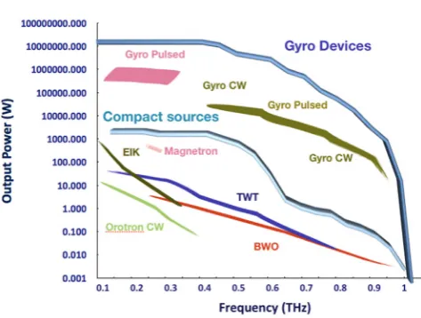
Status. After 110 years, the oldest electron device, the vac-uum tube, has evolved from kHz to THz and mW to MW, as the only practical device for many important applica-tions requiring efficient, compact, medium-to-high power, long-operating-life electromagnetic radiation sources [27]. Vacuum electronic devices (VEDs) convert electrical stored energy into kinetic energy of an accelerated electron beam, which is then converted into electromagnetic field energy with the aid of electromagnetic waveguides or cavities, defined as an interaction zone or circuit (figure 3) [28]. Pres-ently, numerous types of VEDs are available, including trav-eling wave tubes (TWTs), klystrons, magnetrons, gyrotrons and backwards wave oscillators (BWOs), for applications in satellite communications, radar, remote sensing and threat detection, electronic warfare, domestic cooking, industrial heating, space exploration, and scientific research [29, 30]. Generally, the highest attainable frequency is determined by fabrication technologies and the theoretical scaling relation
/(∝ )
Power 1 frequency2 [27, 28]. Due to physical limits on power density management, VEDs present the only practi-cal solution for high power, compact, efficient sources (oscil-lators, amplifiers) of 0.1–1.0 THz radiation [27–31]. VED oscillators and amplifiers (figure 4) have been designed and operated at 0.220–1.0 THz and 10 mW–1 MW with high effi-ciencies (0.5–20% and above) [29–34]. Such performance is unachievable by any other technology [27]. The ability to achieve exceptionally high overall efficiency by spent beam energy recovery is uniquely available to VEDs and not possi-ble with any other compact THz radiation source [28]. Further advances in 0.1–1.5 THz wideband amplifiers and oscillators with watt-level power sufficient to overcome atmospheric attenuation, and dimensions in the range of a few dm3, will enable new generations of multigigabit mobile communica-tions networks (see section 17) and high resolution radar or remote sensing systems that are able to penetrate fog, dust, or other aerosols that obscure shorter-wavelength technologies. Other applications of future high power THz-regime VEDs will include stable frequency sources for imaging (see sec-tion 15), deep space communications, non-invasive health-care diagnosis (see section 12), materials characterization (see section 13), radio astronomy (see section 14), and other scientific research technologies [27–31].
Current and future challenges. In compact VEDs based on classical physics mechanisms, the cross-sectional size of the circuit must scale with the free space wavelength. Therefore, to populate the THz gap, the transverse circuit dimensions of VED sources will typically need to be less than the free space wavelength, i.e. sub-mm [27–31]. Consequently, current and future challenges for compact THz VED sources involve
reliably manufacturing miniature VED circuits that gener-ate and tolergener-ate high internal densities of beam and radiation power. Moreover, to minimize power dissipation, conducting surfaces will need excellent surface quality, including low impurity concentrations, low surface roughness (<20 nm) and moderate grain size (>100 nm) [33]. This means that innova-tions and advances are needed in the following areas:
• Reliable manufacturing of miniature electromagnetic struc-tures (cavities, slow-phase-velocity waveguides) having high quality surfaces and compatible with hard vacuum, high temperature thermal processing during manufacture, and highly precise alignment accuracy (micron-level or <0.1 degree) between components (cathode, beam optics, electromagnetic circuit, and beam collector)
[image:9.595.310.547.65.219.2]• Designs for high current electron beams with sub-mm cross-sections, at least in one transverse dimension Figure 3. Conceptual illustration of a THz vacuum electron amplifier, including the gun (electron beam source), interaction circuit, beam confinement magnets t, beam collector and radiation ports. Oscillators would not need the input port.
[image:9.595.310.547.288.467.2]9 • New cathodes that enable high current density, small
cross-section electron beams with long lifetimes and lower cathode temperatures [28–30, 35]
• Novel circuit designs having strong beam-wave interac-tion at THz frequencies with low voltage electron beams • Compact, low-power, beam optics and confinement,
keeping the beam away from impact on structure walls • Efficient, broadband coupling of radiation out of the
circuit (oscillators and amplifiers) and into the circuit (amplifiers)
• Innovative electromagnetic circuit designs with larger cross-sections that still provide stable, high power, effi-cient generation or amplification of THz-regime radiation.
Advances in science and technology to meet challenges. A new age of opportunity for THz-regime VEDs has emerged with the maturation of highly precise, highly accurate micro-fabrication techniques. These include extensions of conven-tional machining, such as nano-CNC milling, laser-machining, and micro-electro-discharge machining (micro-EDM), as well as the suite of lithographically-controlled etching, depo-sition and assembly techniques derived from micro-electro-mechanical systems (MEMS) research [29, 34]. Examples of the latter include deep reactive ion etching (DRIE), x-ray or ultraviolet LIGA (LIGA is a German acronym for lithography and molding), metallic and dielectric film deposition and dif-fusion bonding with substrate backside alignment [28]. The other recently emergent enablers are the numerous, excep-tional advances in computaexcep-tional hardware, algorithms, and software. High performance, high throughput terascale com-puting is a stable, established technology. Highly sophisti-cated, 1-, 2-, and 3D, time-dependent, multiphysics models of electromagnetic fields, charged particle transport, thermal physics and engineering mechanics have been developed and validated, resulting, in many cases in ‘first-pass’ design suc-cess [28, 31]. These simulation codes now permit quick and accurate predictive evaluation of innovative ideas prior to expensive experimental prototyping and validation.
To realize more powerful, compact, VED sources of THz radiation, scientists and engineers will need to leverage these new fabrication and simulation capabilities and also achieve innovations in electromagnetic THz circuits, beam optics, cathodes, materials and metrology. New circuits exploiting metamaterial or photonic crystal architectures might loosen the requirement for close beam-circuit proximity and still
achieve strong beam-wave interaction [31]. Higher current density cathodes or advanced beam diode focusing optics would enable transporting higher beam power into the very small THz electromagnetic circuit cross-sections [27, 29, 31, 36]. An alternative solution for high power beams in small THz circuits is to generate and focus innovative distributed beams, either laminar sheets or multiple beamlets, that are small in one cross-sectional dimension but spread the cur-rent out in the other cross-sectional dimension [27, 31]. This requires new electromagnetic circuit ideas as well as well-designed magnetic focusing fields to avoid beam instability or to stably guide the many beamlets, respectively. Advances in permanent magnet materials or high temperature super-conductors would enable better magnetic focusing optics with less weight and size. The availability of high-current-density, long-lifetime cold cathodes would enable low-cost, self-aligned integration of the cathode, circuit, and collector dur-ing mass production manufacturdur-ing of micro-VEDs [28, 30]. Advances in metallic 3D printing or new alloys for electro-plating would provide more options for miniature circuit fab-rication. However, the materials and processes would need to yield a circuit with dimensional features <100 µm, tolerance precision ~1 µm, high THz conductivity > 2×10⁷ S m−1, sur-face finish <20 nm [33], and stability against grain growth or stress-induced deformation during high-temperature thermal processing at hundreds of °C. Finally, advances are needed in metrology to characterize and verify the electromagnetic reso-nances or dispersion of THz circuits, precision alignment of components, magnetic field profiles inside the circuits, input and output radiation coupling efficiencies, and the structural, microstructural and electromagnetic properties of the circuit materials before and after manufacturing processes.
4. Accelerator-based sources of terahertz radiation
M Gensch1, P Weightman2 and G P Williams3
1 Helmholtz-Zentrum Dresden-Rossendorf, Institute of
Radiation Physics, Bautzner Landstr. 400, 01328 Dresden, Germany
2 Physics Department, University of Liverpool, Liverpool, L69 7ZE, UK
3 Jefferson Laboratory, 12000 Jefferson Avenue—Suite 21 Newport News, VA 23606
Status. The potential of accelerator driven sources of electro magnetic radiation for scientific research across a wide variety of fields has long been recognized, and exploited internationally, most notably through the development of synchrotron storage rings into unique, broad band multi-user facilities for spectroscopy in the VUV to x-ray regime. The last three decades have seen increasing user interest in utiliz-ing accelerator driven sources for research in the infrared and THz regime. The primary advantages of these sources over table-top sources, such as those described in sections 1and 2 derive from their unique spectral brightness or power and their extreme fields and pulse energies. Historically the first appli-cations of accelerator driven sources exploited the high spec-tral brightness and power available from infrared beamlines at storage rings [37], followed quickly by the use of dedicated user facilities such as IR/THz free electron lasers [38] and finally superradiant radiation [39], where the bunch length of the electrons is less than the wavelength of the emitted radia-tion, from energy recovery linacs (ERLs) [40]. The primary applications of this first generation of sources are brightness-limited spectroscopic techniques such as far-field microscopy or investigations of processes that require high average power such as action spectroscopy [41] or power-limited spectro-scopic studies of e.g. biological systems in water [42]. In the past decade there has been increasing interest in utilizing the extreme scalability of the energy per THz pulse in compact linear accelerator (linac) driven sources. The scientific driver here is research aimed at understanding ultrafast THz driven nonequilibrium dynamics in matter [43] (figure 5). The vision to provide electric fields in the V/Å regime, comparable to the dipole field of an ionic bond, or magnetic fields in the few T regime, commensurate with fields required for alignment of magnetic domains, has led in recent years to considerable technological efforts worldwide [44].
Numerous accelerator-based THz sources are operational worldwide as user facilities. The most common sources are synchrotron infrared beamlines [37] that are available on many synchrotron storage rings. Although the performance of laser-based sources and sources based on thermal emit-ters in their typical frequency range, 1–30 THz, has improved tremendously in the past 10 years, infrared synchrotron beamlines are still very competitive for brilliance limited spectroscopic techniques such as infrared microscopy and ultra-broadband infrared near-field microscopy. Some storage rings can be operated in a special operational mode, called low alpha mode, which via shortening the electron bunches to the few picosecond regime employ superradiant emission
to achieve substantial increases in spectral power below 1 THz [39]. In this mode of operation average powers in the few 10 mW regime have been demonstrated and several break-through experiments on spectr oscopy in correlated materials have been performed (see e.g. [45]). Other projects have used external lasers to slice or to modulate the electron bunch struc-ture to induce superradiant THz emission [46]. The first ERL source became operational in 2001 [40], and these sources provide radiation in a similar frequency range and with sig-nificantly more power than can be obtained on a synchrotron. Average powers of the order of 10 W and peak powers in the kW regime have been obtained. This is possible because they are based on the new superconducting radio frequency (SRF) technology that enables the operation of linear accelerators at previously unprecedented duty cycles. There are few oper-ational facilities but the potential of these sources has been demonstrated in a number of experiments [42, 47]. There is a much wider use of low-gain free electron lasers. Their pulsed, narrow-band tunable radiation is used in the chemical and life sciences to study the infrared spectrum of dilute systems such as clusters or individual molecules by means of the so called action spectroscopy [41]. Some facilities use SRF technology and hence provide average powers in the few 10 W to even kW regime. Those focus on specific spectroscopy applica-tions in solid state physics that benefit from high flux such as nearfield microscopy [48] or studies of samples under extreme conditions e.g. high pres sure or high magnetic fields [49]. The combination of an ERL and a THz FEL provides a particular high power source tunable over a narrow frequency range.
11 one recent example being THz selective control of surface chemistry [50]. The record THz fields have so far have been obtained at large linear accelerators and at relatively low rep-etition rates [51] limiting the application to a few demonstra-tion experiments [50]. A general challenge for time-resolved experiments at accelerator-based THz sources like FELs or superradiant linac-based sources, remains the synchronization to external laser systems which is currently limited to the few picosecond regime.
Advances in science and technology to meet chal-lenges. There has recently been a proposal for a novel variable pulse length storage ring concept [52] which if suc-cessful would make it possible to generate THz pulses using the low alpha mode on a synchrotron while preserving the beam properties for the typical XUV and x-ray applications. This would result in a significant increase in the available beamtime on synchrotrons for applications in the low THz frequency range. In the field of linac-based superradiant high-field THz sources there are more than ten projects that are currently proposed or are being developed worldwide based on the development of compact sources of high-field THz radiation. Sources with linacs of only a few meters in
length are proposed or are already being commissioned [44]. Some projects aim to combine high fields of the order of MV cm−1 with high repetition rates up to the MHz regime. These sources are based on compact quasi-continuous wave SRF linac technology and have demonstrated impressive progress. Since SRF technology is the basis of several large scale proj-ects (European X-FEL, LCLSII or ILC) it is expected that in the long term high repetition rate high-field superradiant THz sources will be made more compact, reliable and cost efficient. It is also expected that advances will be made in addressing the timing problems in synchronising SRF lin-acs and external lasers. Several schemes have demonstrated sub 10 fs resolution via post mortem correction of the arrival time jitter. Most recently sub 100 fs synchronization has been demonstrated by active feedback of the accelerator itself. A demonstration THz control experiment, achieving sub 30 fs time resolution, recently showed the enormous advantage of the combination of high-field and high repetition rate for driving coherent dynamics in solids. Particularly interest-ing is the fact that it was also shown that multiple sources can be operated from one electron beam making multi beam user facilities possible [53]. A first user facility of this type is expected to become operational in 2016 at the HZDR in Germany and several similar projects are being discussed worldwide (e.g. at DESY/Germany, FERMI/Italy, SLAC/ USA, SACLA/Japan).
[image:12.595.51.290.74.185.2]Concluding remarks. The development of accelerator-based sources of THz radiation has evolved over the past years towards user facilities that provide either unprecedented high average powers, up to the few 10 W and even kW regime, or more recently high peak fields and/or peak fields at high repetition rates up to 10 MV cm−1 and beyond. These sources complement laser-based and other table-top THz sources, which are limited to lower average powers, lower peak fields and lower repetition rates. The applications of such sources have widened from the brilliance-limited THz spectroscopy applications of the early days towards flux-limited experi-ments and experiexperi-ments investigating nonlinear dynamics driven by extreme transient THz fields.
Figure 5. THz-driven chemistry—a quasi-half-cycle, broadband superradiant THz pulse with peak fields of ~1 V nm−1
5. Photoconductive devices for THz time-domain spectroscopy
E Castro-Camus
Centro de Investigaciones en Optica A.C., Loma del Bosque 115, Lomas del Campestre, Leon, Guanajuato 37150, Mexico E-mail: [email protected]
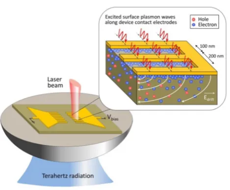
Status. As described in detail in section 8, a central devel-opment that allowed spectroscopists wider access to the THz band was the creation of time-domain spectroscopy in the 1980s. The key device that allowed the reliable generation and detection of broadband THz radiation was the photo-conductive switch [54]. Since their initial introduction, these devices have evolved dramatically. The original semiconduc-tor they were fabricated on, Si-on-sapphire, was replaced by low-temperature-grown GaAs [55]. Other materials such as alloys of InGaAs [56] and even graphene-based materials [57] have been used showing promising improvements of this technology, expanding compatibility from Ti:sapphire (~800 nm)-based laser excitation to wavelengths suitable for rare-earth-doped fiber lasers (1050 nm–1550 nm). These pro-vide a cheaper, more portable, more stable and potentially more reliable source of ultrashort pulses. Even individual semiconducting nanoparticles [58] have been used to make photoconductive detectors, opening the possibility of fabricat-ing micrometric and nanometric electronic circuits or optical systems that incorporate them. Currently the dynamic range of photoconductive device based systems has reached up to 90 dB and their typical spectrum usually covers from 0.05 THz to 2–6 THz [56].
In addition to the changes in the semiconductors used, the contacts have evolved from relatively simple bow-tie, dipole or strip-line structures, to rather sophisticated geometries incorporating features in the hundreds of microns to few millimetres scale that act as antennas and mediate the cou-pling of terahertz radiation in and out of the device, as well as nanometric features (see figure 6) that improve the optical radiation coupling into the semiconductor [59] and limit the semiconductor–metal charge transit time [60]. Some designs have incorporated additional contacts allowing the detection of different components of the THz electric field and, at its time, making polarization resolved TDS possible [61]. This technique provides twice as much information in a single tera-hertz measurement and removes the possibility of ambigui-ties and artefacts caused by anisotropic properambigui-ties of materials such as birefringence and optical activity (see figure 7).
Current and future challenges. The one most important tech-nological challenge that photoconductive emitters face these days is their cost-effective large scale production viability. Low-temperature GaAs (or InGaAs) is still the most widely used material for photoconductive devices, however its fabri-cation has two major disadvantages. Firstly, the semiconductor properties are difficult to reproduce, even when grown under the same nominal conditions in the same reactor. Secondly, its growth requires being performed in molecular-beam-epitaxy
(MBE) machines, which is an expensive method for large scale production of terahertz devices.
Although some approaches like the incorporation of nano-metric gaps could improve significantly the performance of photoconductive detectors and eliminate the need for short-carrier-lifetime materials, their large scale production also requires very high resolution fabrication techniques such as electron beam lithography, which is also unlikely to be imple-mented for large scales cost-effectively.
The development of compact and on-chip THz oscopy systems [62], which promise to expand THz spectr-oscopy into new applications, will be a driver for the further development of photoconductive THz devices. There will be a continued drive for more compact femtosecond lasers system and THz sources which in turn will stimulate the development of THz devices optimised for these systems.
Other future applications of THz-TDS in materials analysis and structural biology will require further advances in polari-sation resolving THz detectors (see sections 11 and 13). The challenge here is to develop detectors with good enough polar-isation sensitivity to be used in vibrational circular dichroism spectrometers [63].
Advances in science and technology to meet challenges. On the material front, ion-implanted [64], nanoscale [58], and nanostructured [56] semiconductors are showing promising results for replacing low-temperature grown materials, and the quality of materials grown by chemical-vapor-deposition, atomic-layer-deposition and other techniques, more economi-cal than MBE, is improving.
[image:13.595.314.549.61.255.2]13 production of devices with features in the scale of ~10 nm, which would be ideal for the fabrication of some of structures such as plasmonic nanostructures.
Concluding remarks. Terahertz photoconductive devices have evolved dramatically since their introduction in the
[image:14.595.139.470.63.217.2]1980s. The bandwidth, power and reliability of these devices improved with the use of novel semiconductor materials and contact structures. The viability of fabricat-ing these devices at industrial scales is an issue still befabricat-ing addressed, but promising solutions can be foreseen in the years to come.
6. Components for terahertz imaging
D R S Cumming1, F Simoens2, I Escorcia-Carranza1
and J Grant1
1 Microsystems Technology Group, School of Engineering, University of Glasgow G12 8LT, UK
2 CEA-Leti MINATEC, 17 rue des Martyrs, Grenoble, Cedex 9 38054, France
E-mail: [email protected]
Status. Terahertz imaging has been demonstrated using a wide range of methods. These include pulsed time-domain (PTD) and continuous wave (CW) technologies, single detec-tor scanned systems, arrays and focal plane arrays (FPAs). As described in the Friis equation, the overall performance of an imager is determined by its optical properties including source power, system losses, and detector sensitivity. Whatever the means of implementation, all systems rely on the brightness of the illumination source deployed and the responsivity of the detector.
Time-domain systems (as described in section 8) rely on high-speed rectification of a short pulse using either a pho-toconductive switch or a crystal such as ZnSe. They have a commensurately high frequency bandwidth in the terahertz spectrum, but typically illumination power is weak, a prob-lem that is overcome by using synchronous detection (see section 5). A valuable attribute of these systems is that they provide depth ranging and the potential for spectroscopy. Owing to the low brightness of the sources, image acquisition times are typically quite slow.
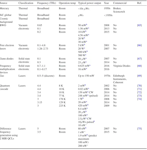
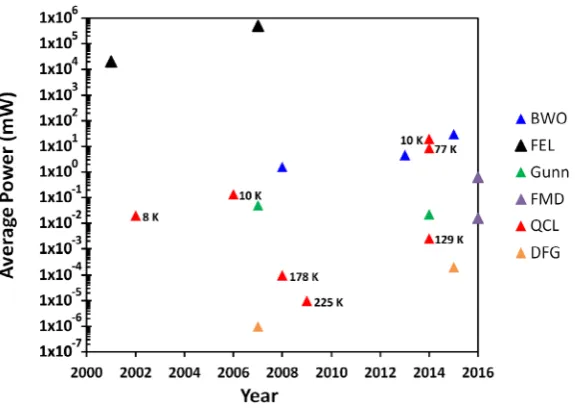
Scalar systems are simpler to construct and are only achievable with relatively high power sources. For fre-quencies of approximately 1 THz and below, CW sources derived from microwave electronics such as Gunn oscil-lators, backward wave oscillators and diode-multiplied sources can be used. At longer wavelengths, CW sources include large methanol vapour lasers. Quantum cascade lasers are excellent in the mid-IR but for terahertz require cooling and pulsed mode operation, as discussed in sec-tion 1. Table 1 and figure 8 summarise the performance of source technologies and the trend over time towards enhanced performance.
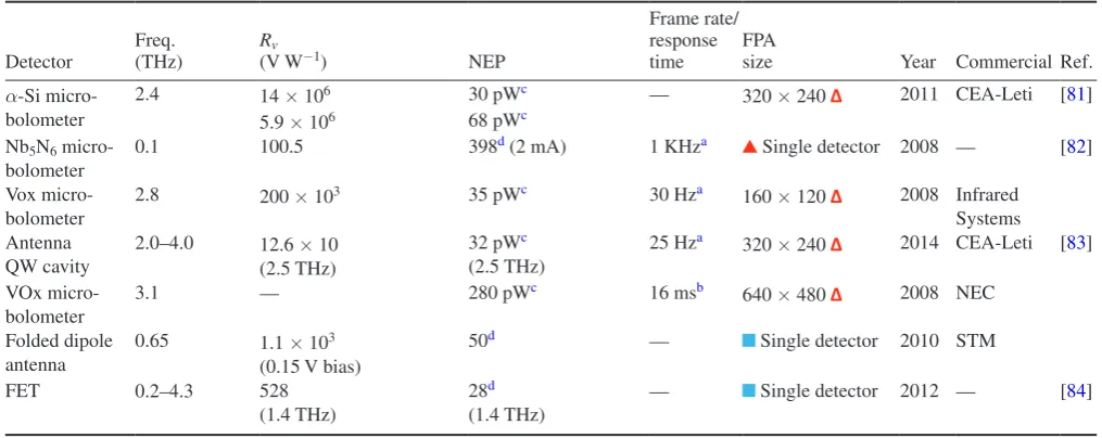
Detector technologies are improving in terms of noise equivalent power (NEP), responsivity (Rv) and potential for
integration, e.g. into focal plane arrays. Table 2 and figure 9 show representative data for a range of detector technologies at room temperature, and progress over recent years. Several of the detectors have been designed specifically for use in imaging applications and we have specified array size and electronically achievable frame rate where relevant. Note that noise limitations and low source power means that these rates are not always achieved in practice.
Current and future challenges. Many application areas have emerged for terahertz imaging, and this has motivated a great deal of research in the underpinning technology. The breadth and societal value of the applications is very great, and are briefly summarised as follows:
• Stand-off detection of hidden objects and weapons • Non-invasive medical and dental diagnostics
• Detection of cracks and defects in materials e.g. solar panels, plastics
• Non-destructive rapid fault isolation in IC packages • Drug discovery and formulation analysis of coatings and
cores
• Non-contact imaging for conservation of paintings, manuscripts and artefacts
• Monitoring of crop and plant hydration levels
The challenge for imaging system developers is to devise miniature systems suitable for use in the field. These may be handheld devices or, for example, units for use on remotely operated vehicles (ROVs). It will therefore be necessary to produce high power, low cost and small source technologies that do not require cryogenic cooling. Similarly, there will be a requirement for uncooled detectors. Since, as already noted, full system performance accounts for the attributes of sources, system losses and sensor performance the development of sources and detector technologies will advance in tandem.
Advances in science and technology to meet chal-lenges. Future expectations for terahertz imaging systems include video rate imaging (at least 25 fps) at VGA resolution. Further into the future, HD format will be the normal expecta-tion for any imaging system. Image resoluexpecta-tion (as opposed to display resolution), noise and dynamic range are all expected to improve. These improvements will rely on advancement in source, detector and optical/system design technology. Spe-cifically, compact, room temperature terahertz sources in the region of 10 mW average power are essential in order to enable stand-off imaging at distances greater than 1 m. Such sources when coupled with a Si CMOS FPA would render a low-cost THz camera (we estimate <US$5 K per unit) that could find wide spread use in applications such as stand-off detection of hidden objects and non-invasive medical (e.g. oncology) and dental diagnostics. For synchronous detection, current devel-opments are aimed at decreasing acquisition times by using multi-channel systems and on employing quasi time domain spectroscopy (QTDS) by replacing the costly femtosecond laser with an inexpensive multimode laser diode. There will also be advances in sophisticated imaging modalities includ-ing near field imaginclud-ing for high resolution imaginclud-ing and confo-cal imaging that promises depth information using CW sconfo-calar imaging technologies.
15 frame rate; resolution; dynamic range; stand-off distance; and reduced size and weight. As can be seen from the review data presented here it is likely that semiconductor technologies will play a vital role and in particular we highlight potential
[image:16.595.56.546.75.576.2]advances in semiconductor laser sources and CMOS-based detector technologies. There will also be a need for further advances in passive components based on antenna, lens and metamaterial theory, design and implementation.
Table 1. Terahertz sources.
Source Classification Frequency (THz) Operation temp Typical power output Year Commercial Ref.
Mercury Thermal Broadband Room ~10s µWs 1950s Bruker,
Sciencetch
SiC globar Thermal Broadband Room µWs <1950s
Cosmic background
Thermal Broadband Room
BWO Vacuum
electronic
0.65 Room 50 mWb 2008 No [65]
0.1 Room 1.56 mWa 2013 No
0.2 Room 10 kWb 2015 No
4.56 mWa 20 Wb 30 mWa Free electron
lasers
Vacuum electronic
0.1–4.8 Room 5 kWb 2001 No [66]
1.28–2.73 Room 20 Wa 2007 No
500 kWb 500 Wa Gunn diodes Solid state
electronic
0.1 Room 50 µWa 2007 No [67]
0.3 Room 23 µWa 2014 No
Frequency multiplication devices
Solid state electronic
0.7–1.1 Room 0.625 mWa 2016 Virginia Diodes [68]
0.1–0.17 Room 16 mWa 2016
Gas Lasers 0.5–5 (discrete) Room Up to 150 mW 1970s Edinburgh
Instruments, Coherent
[69]
Quantum cascade
Lasers 4.4 8 K 2 mWb 2002 No [70]
4.4 10 K 0.02 mWa 2006 No [71]
3.4 10 K 139 mWa CW
248 mWa (pulsed) 1 Wb
20 mWa 420 mWb 8.4 mWa 20 µWb 100 nWa 2.5µWa CW 10µWs pulsedb 10 nW+
2014 No [72]
3.4 77 K 2014 No [73]
3 178 K 2008 No [74]
3.15 129 K 2014 No
3 225 K 2009 No
Difference frequency generation using 2 MIR QCLs
Lasers 5 Room 80 nWb 2007 No [75]
3.5 Room 1 nW+ 2015 No
1.9 mWb (predict maximum 100 mW) 200 nW+
Figure 8. Progress of terahertz sources over recent years: BWO = backward wave oscillator ( ), FEL = free electron laser ( ), FMD = frequency multiplier devices ( ), gunn diodes ( ), QCL = quantum cascade laser (at 10 K unless otherwise stated) ( ), DFG = difference frequency generation ( ). All data are at room temperature unless otherwise stated.
Table 2. Terahertz detectors.
Detector Freq. (THz) R(V Wv −1) NEP
Frame rate/ response
time FPA size Year Commercial Ref.
Schottky barrier diode (SBD)
0.11–0.17 0.9–1.4 1.1–1.7
2000 100 100
13.2d 113.7d 113.7d
42 nsb 25 nsb 25 nsb
Single detector 2007 VDI
SBD 0.86 273 42d −1 µsb Single detector
4 × 4
2013 — [76]
0.28 336 290 pWc
Photo conductive
0.1–4.0 — — — Single detector 2011 EKSPLA
1985 Folded
dipole antenna
0.6–1.0 800 (1.027 THz) 66d (1.027 THz) — Single detector 2011 STM
FET FPA
0.7–1.1 115 × 103 (0.856 THz)
12 nWc (0.856 THz)
25 Hza 32 × 32 2012 STM
VOx micro-bolometer
2.5 72 × 103 (2µA) 5620 (100 nA)
37d (15 Hz mod.)
3.6 µWc 68 ms
b
194 msb 5 × 5 Single detector 20132015 —— [[7778]] 2.5
Bolometer 4.25 — 24.7 pWc 50 Hza 384 × 288 2013 INO
2.54 — 76.4 pWc
Golay cells 0.2–20 10 × 103
(12.5 Hz modulation)
10 × 103d 25 msb Single detector 2009 Microtech
Micro- bolometer
1.0–7.0 — <100 pWc (4 THz) 30 Hza 320 × 240 2014 NEC
LiTaO3 0.1–300 — 96 nWc (50 Hz mod.) 50 Hza 320 × 320 2014 Ophir
Photonics Pyroelectric
Pyroelectric 0.3, 1.0, 3.010 18.3 × 10³ (10 Hz mod.)
440d 10 Hza Single detector 2009 QMC
Hot electron 0.89 0.095 7.4 × 10³d 200 Hza Single detector 2007 — [79]
Bolometer SixGey:H micro- bolometer
0.934 170 200d 1 msb Single detector 2010 — [80]
[image:17.595.47.554.329.704.2]17 Table 2. Continued
Detector Freq. (THz) R(V Wv −1) NEP
Frame rate/ response
time FPA size Year Commercial Ref.
α-Si micro-bolometer
2.4 14 × 106 30 pWc — 320 × 240 2011 CEA-Leti [81]
5.9 × 10⁶ 68 pWc
Nb5N6 micro-bolometer
0.1 100.5 398d (2 mA) 1 KHza Single detector 2008 — [82]
Vox micro-bolometer
2.8 200 × 103 35 pWc 30 Hza 160 × 120 2008 Infrared
Systems Antenna
QW cavity
2.0–4.0 12.6 × 10 (2.5 THz)
32 pWc (2.5 THz)
25 Hza 320 × 240 2014 CEA-Leti [83]
VOx micro-bolometer
3.1 — 280 pWc 16 msb 640 × 480 2008 NEC
Folded dipole antenna
0.65 1.1 × 10³ (0.15 V bias)
50d — Single detector 2010 STM
FET 0.2–4.3 528
(1.4 THz)
28d
(1.4 THz) —
Single detector 2012 — [84]
a Achieved imaging frame rate.
b Response time of individual sensor or pixel. c NEP for arrays operating in video modes. d NEP for single detectors (pW (√Hz)−1).
[image:18.595.156.444.360.540.2]7. Passive THz components
Stepan Lucyszyn1, Makoto Kuwata-Gonokami2
and Kuniaki Konishi2
1 Centre for Terahertz Science and Engineering, Department of EEE, Imperial College London, UK
2 Department of Physics, University of Tokyo, Japan
Status. Coherent time-domain spectroscopy and non-coher-ent frequency-domain radiometry are two examples of ultra-broadband THz applications. In general, where performance is paramount, quasi-optical front-end implementations are preferred over the use of guided-wave structures because of the need to minimizing material loss contributions. How-ever, the relentless advancements in achieving ever-higher performance sources and detectors are beginning to relax the requirements for passive components in the lower region of the cost-performance application space. Moreover, with the drive to make complete systems smaller, lighter and cheaper, guided-wave structures offer distinct advantages over their quasi-optical counterparts; the former has inherent advan-tages in terms of providing better isolation, a wider choice of implementation solutions and can be more easily integrated with active devices without the need for optical alignment accuracy. While transmission lines (e.g. microstrip, coplanar waveguide and coplanar strip) represent the obvious solutions for realizing passives on hybrid and monolithic millimetre-wave integrated circuits, in general, they can suffer from high substrate and radiation losses. In addition, their relatively high conduction current densities result in high dissipative (ohmic) losses at terahertz frequencies. As a result, only low qual-ity factor/high attenuation components are possible at room temperature. Usually, to achieve best performance at room temperature, off-chip resonator/filter solutions are needed. Nevertheless, many papers report on the predicted simulated performance of transmission line-based monolithic THz fil-ters; few give measured results. One notable exception is the work by Nagel et al [85]. Here, a 0.61 THz second-order thin-film microstrip coupled-line band-pass filter is demonstrated. With gold metallisation and benzocyclobutene dielectric lay-ers, on a silicon substrate having an integrated photoconduc-tive switch, the filter exhibits a measured loaded quality factor of ~10 and insertion loss of −11 dB [85].
Surface plasmon waveguides suffer from relatively poor mode conversion efficiency and high attenuation due to ohmic losses. Nevertheless, because of their tight field confinement, near-field enhancement characteristics and ability to over-come diffraction limits, devices based on the surface plasmon polariton (SPP) offer the potential for future SPP-based inte-grated circuits at THz frequencies.
Three examples of high-performance guided-wave tech-nologies used at terahertz frequencies are considered; (1) all metal, (2) metal-dielectric and (3) all dielectric. In general, since dielectric losses can be much lower than those associ-ated with normal room-temperature conductors, lower loss/ high quality factor passives can be realized by minimizing conduction current densities and ideally avoiding the use of
metals altogether. All three relatively low loss waveguide technologies have been used to demonstrate key components (e.g. power couplers and resonators, used in high performance impedance matching networks, filters and antennas). (1) Metal-pipe waveguides have historically been around for over a century. However, it is only since 2016 that international standards were agreed for operating above 0.1 THz; the IEEE P1785 Working Group proposed standards up to 5 THz [86]. This recognises the growing importance of this guided-wave medium for industrial applications. Monolithic forms of hol-low (air-filled) metal-pipe rectangular waveguide technologies have been around since the early 1990s, first introduced by JPL/Caltech for silicon integration with active devices. Since then there has been a raft of technologies that have moved ever higher in frequency and/or with lower manufacturing costs. Without introducing additional functionality but still maintaining high performance, the University of Birmingham (UK) is currently replacing expensive bulk micromachining of silicon by surface micromachining of SU-8 photoresist sac-rificial building materials, recently demonstrating split-block waveguides from 0.5 to 0.75 THz, with integrated 3rd order band-pass filters. This idea follows on from a similar ‘ snap-together’ technology introduced by the UK’s EPSRC-funded Terahertz Integrated Technology Initiative (TINTIN) research programme (a collaboration between the Universities of Bath, Reading, Nottingham and Leeds). In 2006, TINTIN demon-strated slotted H-plane sectoral horn antennas at 1.6 THz. (2) Oversized dielectric-lined metal-pipe rectangular and circular waveguides operating with a quasi-single mode of propaga-tion were first introduced in 1963 and subsequently demon-strated losses as low as 0.0037 dB m−1 at 150 GHz with ~10 wavelength diameter structures lined with a low-loss di electric and below 1 dB m−1 above ca. 0.3 THz with ~20 wavelength diameter structures lined with a high-loss dielectric. More recently, a silver-coated PTFE (Teflon™) circular waveguide has been demonstrated, having a measured transmission loss of ~20 dB m−1 across the ca. 1.0–1.6 THz frequency range [87]. (3) Rectangular dielectric waveguide components avoid skin-effect related losses altogether, but still suffer from poor isolation. To improve field confinement, photonic crystal waveguides exploit Bragg reflections at the boundaries of di electric waveguides. An example of a bendable Topas poly-mer photonic crystal fibre was reported by Nielsen et al, hav-ing a loss of <10 dB m−1 at 0.6 THz [88]; while an photonic crystal resonator that can potentially combine electric field sensing with integrated electronics has been demonstrated in high-resistivity silicon [89].
19 ratio is inferior and they are more expensive than those in the optical region. Recently, new THz polarizers have been devel-oped using exotic materials such as liquid crystals and carbon nanotubes offering extinction ratios as high as 50 dB, which is comparable to those at shorter wavelengths [90]. Wave plates represent another important component for polariza-tion control. The quartz crystal is commonly used because it is transparent and has birefringence in the THz frequency region. However, crystal wave plates only work at a single frequency. Recently, Nagai et al proposed and demonstrated a new scheme to realize broadband wave plates, which works from 2.0 to 3.1 THz by utilizing a stacked waveguide struc-ture [91]. Filters are indispensable components in spectr-oscopy. Metal mesh filters have been used for a long time at millimetre-wave frequencies, but have recently extending into the sub-millimetre-wave (i.e. THz) region and is considered a class of metamaterials or metasurfaces [92].
Current and future challenges. Existing guided-wave struc-tures and quasi-optical component technologies can achieve reasonable performance at terahertz frequencies, in terms of field confinement, transmission loss and frequency disper-sion, over a broad spectral range. However, even with high-end applications, size, mass and cost may still pose serious challenges. Moreover, for ubiquitous applications, the cost of achieving even moderate performance must be addressed in its passive components and associated subsystems. This becomes even harder to address when component tuneabil-ity and subsystem reconfigureabiltuneabil-ity (found at microwave and millimetre-wave frequencies) is required in future multifunc-tional systems.
Advances in science and technology to meet challenges. In the lower region of the cost-performance application space, with voxel sizes heading towards 10 microns, additive manufactur-ing technologies that include 3D printmanufactur-ing (e.g. 3D printed plas-tic structures with optional gold-copper surface deposition) are moving into the terahertz band. In the upper region of the per-formance-cost application space, traditional micromachining
and microelectromechanical systems (MEMS) technologies can increase performance and provide additional functional-ity, respectively. Tuneable terahertz components would other-wise be difficult to realize within an integrated environment, as the introduction of mechanical tuning mechanisms gener-ally increases both losses and the size of the overall subsys-tem. Sandia National Laboratories in the U.S. recently reported a 3 THz meandered metal-pipe rectangular waveguide with H-plane horn antenna coupling, manufactured using conven-tional surface micromachining [93]. A scanning electron micro-graph of this structure is shown in figure 10. With electroplated gold walls, the measured transmission loss is approximately 1.3 ± 0.1 dB mm−1 or 0.12 dB/wavelength at 3.1 THz.
In order to meet future challenges of providing integrated tuneable components and reconfigureable subsystems, without the use of either conventional electronic or (micro)mechani-cal switches, which can be cumbersome at THz frequencies, a solution was proposed by Imperial College London in the UK [94]. Known as a reconfigureable terahertz integrated architecture (RETINA), metal-pipe rectangular waveguide having pseudo-conducting (plasma) sidewalls are generated within high-resistivity silicon wafers, patterned by program-mable laser or LED light sources. A concept illustration of how a RETINA phased array antenna can incorporate trans-mit-receive duplexer switching and tuneable time steering, by simply changing the pattern of light, is shown in figure 10.
[image:20.595.81.522.59.236.2]only possible but has already been demonstrated at THz fre-quencies. For example, the University of Tokyo in Japan dem-onstrated handedness-switching of chirality with a ca. 1 THz metamaterial, shown in figure 11, which can be used to real-ize an active THz polarization modulator [96]. With the latter, within a semiconductor, photo-induced carriers can introduce individual defects within a metamaterial or even generate a complete 2D ‘virtual’ metamaterial, which can be controlled by changing the light source patterns.
Concluding remarks. With the relentless advances in the per-formance of active devices and circuits that make up sources,
[image:21.595.65.522.63.167.2]amplifiers, active modulators and detectors, the associated passive components (implemented with either guided-wave structures or free-space quasi-optics) will ultimately limit the overall performance of front-end THz subsystems. Existing and emerging passive component technologies, used to per-form vital functions (e.g. within impedance/amplitude/phase matching networks, power couplers, filters, antennas, polar-izers and even switches), must find their niche location(s) within the ever-expanding cost-performance application space. Be-spoke passive solutions will be needed to keep pace with developments in active technologies, ideally without the need for cryogenic cooling.
![Figure 5. THz-driven chemistrysuperradiant THz pulse with peak fields of ~1 V nm—a quasi-half-cycle, broadband −1 (10 MV = cm) and a peak frequency of 10 THz induces CO oxidation on the coadsorbed phase of CO and O on Ru(0 0 0 1) in ultrahigh vacuum (UHV) at a temperature of 300 K [50] (reused by permission of H Ogasawara/SLAC and APS/Joan Tycko)).](https://thumb-us.123doks.com/thumbv2/123dok_us/7743963.165714/12.595.51.290.74.185/chemistrysuperradiant-broadband-oxidation-coadsorbed-ultrahigh-temperature-permission-ogasawara.webp)

![Figure 10. Left: surface micromachined integrated 3 THz meandered metal-pipe rectangular waveguide with H-plane horn antenna coupling [93]](https://thumb-us.123doks.com/thumbv2/123dok_us/7743963.165714/20.595.81.522.59.236/figure-surface-micromachined-integrated-meandered-rectangular-waveguide-coupling.webp)
![Figure 11. MEMS spirals [96] (a): microphotograph in the pre-actuation state, (b) microphotograph in the on-actuation state, and (c) illustration of THz polarization modulator operation](https://thumb-us.123doks.com/thumbv2/123dok_us/7743963.165714/21.595.65.522.63.167/microphotograph-actuation-microphotograph-actuation-illustration-polarization-modulator-operation.webp)
