GaN/AlGaN multiple quantum wells grown on transparent and conductive (-201)-oriented β-Ga2O3 substrate for UVvertical light emitting devices
I. A. Ajia,1 Y. Yamashita,2 K. Lorenz,3 M. M. Muhammed,1 L. Spasevski,4 D. Almalawi,1 J. Xu,1
K. Iizuka,2 Y. Morishima,2 D. H. Anjum,5 N. Wei,5 R. W. Martin,4 A. Kuramata,2 and I. S.
Roqan1,a)
1King Abdullah University of Science and Technology (KAUST), Physical Sciences and
Engineering Division, Thuwal, 23955, Saudi Arabia.
2Tamura Corporation and Novel Crystal Technology, Inc., Sayama, Saitama 350-1328, Japan.
3INESC-MN, IPFN, Instituto Superior Técnico, Campus Tecnológico e Nuclear, Bobadela LRS,
Portugal.
4Department of Physics, SUPA, University of Strathclyde, Glasgow, G4 0NG, United Kingdom.
5King Abdullah University of Science and Technology (KAUST), Imaging and Characterization
Core Laboratory, Thuwal, 23955, Saudi Arabia.
GaN/AlGaN multiple quantum wells (MQWs) are grown on a 201 -oriented β-Ga2O3
substrate. The optical and structural characterizations of the MQW structure are compared with a
similar structure grown on sapphire. Scanning transmission electron microscopy and atomic force
microscopy images show that the MQW structure exhibits higher crystalline quality of
well-defined quantum wells, when compared to a similar structure grown on sapphire. X-ray diffraction
rocking curve and photoluminescence excitation analyses confirm a lower density of dislocation
defects in the sample grown on β-Ga2O3 substrate. Detailed analysis of integrated and
resolved photoluminescence measurements shows that the MQWs grown on the β-Ga2O3 substrate
are of higher optical quality. Our work indicates that 201 -oriented β-Ga2O3 substrate can be a
III-nitride semiconductors are known for their mechanical durability, as well as wide and direct
bandgap characteristics, making them ideal for many optoelectronics and photonics applications.
However, their performance as light emitting devices is presently limited by excessive threading
dislocation (TD) defects caused by lattice mismatch with suitably transparent substrates, such as
Al2O3 (sapphire) with a lattice mismatch of ~16% with GaN.12 One possible replacement candidate
that has recently received significant attention is the transparent and conductive 201 -oriented β
-Ga2O3 substrate.3-6 Its main advantages stem from its lower effective mismatch with GaN
(~4.7%),3 making it a promising candidate for mitigating the problem of high defect densities
typically characterizing III-nitride materials grown on Al2O3. Furthermore, β-Ga2O3 is a
conductive oxide with characteristic transparency (down to 260 nm) in the UV region, which is
highly beneficial for UV vertical light emitting diodes, including vertical cavity surface emitting
lasers (VCSELs).5,7 This contrasts it sharply with other alternatives, such as conductive SiC that
lacks UV transparency,8 and GaN that is not as transparent for deep UV as β-Ga2O3 (and is thus
inadequate for AlGaN growth) and is impossible to produce on large scale at reasonable costs.11
Moreover, β-Ga2O3 is relatively cost-effective and easy to grow.9,10 GaN, InGaN and AlGaN layers
have been previously grown on (100)-oriented β-Ga2O3 by metal organic chemical vapor
deposition (MOCVD)12,13 and molecular beam epitaxy14,15 but the material quality was poor
compared to that grown on Al2O3. More recently, the quality of the GaN and AlGaN epitaxial
layers was slightly improved by employing facet controlled growth on β-Ga2O3.16 However, the
authors reported that, due to the strong cleavage nature of the (100) plane of β-Ga2O3, the epilayer
uncontrollably peeled off from the substrate, resulting in unstable devices. Therefore, 201
-oriented β-Ga2O3 is well positioned as a suitable alternative substrate for use in vertical emitting
a high-efficiency InGaN/GaN multiple quantum well (MQW) vertical LED on 201 -oriented β
-Ga2O3 substrate.17 However, UV emitting GaN/AlGaN MQW structure grown on 201 -oriented
β-Ga2O3 substrate has not yet been achieved.
In this work, we study the structural and optical properties of GaN/AlGaN MQW structures
grown on 201 -oriented β-Ga2O3 substrate. We compare their properties with MQWs grown on
Al2O3. We demonstrate that 201 -oriented β-Ga2O3 is a substrate with potential value for the
growth of vertical UV emitting devices.
The MQW structure (Sample S1) was grown by MOCVD on 201 -oriented β-Ga2O3.
Trimethylgallium, trimethylaluminum and ammonia were used as precursors for epilayer growth.
The growth commenced with a 2 nm low-temperature AlN buffer layer grown on 201 -oriented
β-Ga2O3 substrate at 550 °C. A 100 nm n-Al0.75Ga0.25N layer was then grown at 1020 °C, followed
by a 900 nm thick n-Al0.30Ga0.70N layer at 1120 °C. The overgrown III-nitride epilayers crystalized
with the c-plane (0001) parallel to the 201 plane of the monoclinic β-Ga2O3, as shown
elsewhere.3 N
2 and H2 were used as the carrier gasses for the AlN buffer and the n-AlGaN layer,
respectively. Subsequently, 3×GaN MQW and 4×Al0.2Ga0.8N multiple quantum barriers (MQBs)
with 3 nm and 10 nm nominal thicknesses, respectively, were overgrown on the AlGaN layer at
900 °C. The pressure inside the reactor was maintained at 100 mbar throughout the growth process.
For comparison, a similar MQW structure (Sample S2) was grown on c-sapphire ((0001)-Al2O3)
under the same conditions, with the exception of the AlN buffer layer, which was 8 nm thick for
growth optimization.
High resolution X-ray diffraction (XRD) was performed on a Bruker AXS D8 Discover
diffractometer using Cu Kα1 radiation. A Göbel mirror and a 2-bounce Ge (2 2 0) monochromator
scintillation detector in the secondary beam. Scanning transmission electron microscopy (STEM)
was performed by Titan Themis Z 40−300 TEM. The surface morphology of the samples was
examined by Agilent 5400 atomic force microscopy (AFM). Time-integrated photoluminescence
(PL) was performed using a frequency-doubled Ar+ CW laser at 244 nm (an excitation power of 5
mW and a spot size of ~60 µm). The signal was detected by Andor SR-303i spectrograph and
charge-coupled device (CCD) camera. The time-resolved photoluminescence (TRPL) was
performed using frequency-tripled Ti:Sapphire pulsed laser (266 nm) with a pulse width of 150 fs
and a pulse rate of 76 MHz. The Ti:Sapphire laser had an average excitation power of 3 mW and
was focused to a diameter of ~60 µm, measured by a Gentec beam profiler. The signal was detected
by an Acton spectrograph and Hamamatsu C5680 streak camera operating in a synchroscan mode
with a temporal resolution of 2 ps. The samples were mounted in a closed-cycle He cryostat to
vary the temperature between 6 K and room temperature (RT). Photoluminescence excitation
(PLE) measurements were performed at RT using an Edinburgh Instrument FLS 980 fluorescence
spectrometer attached to a 1000 W xenon arc lamp. Cathodoluminescence (CL) measurements
were performed using the FEI Quanta 250 scanning electron microscope (SEM) with an electron
voltage of 5 kV. SEM was coupled to a spectrograph and a CCD camera.
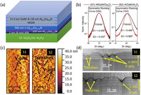
Fig. 1(a) shows the structural schematic of both samples. Fig. 1(b) provides the symmetric
and asymmetric XRD rocking curve (RC) plots. The symmetric RC plots around the (004)
reflection for the two samples are similar. However, the AlGaN layer grown on Al2O3 (S2) shows
a considerably broader peak for the (104) asymmetric reflection (measured in skew symmetry),
suggesting a higher density of edge dislocations than that in the layer grown on 201 -Ga2O3 (S1),
as asymmetric reflection RCs are broadened by edge dislocations, whereas symmetric reflection
Fig. 1(c) shows the false color AFM topography of S1 and S2, both of which exhibit
extensive surface defects. S1 is characterized by high densities of V-pit defects (Fig. S1 in
Supplementary Material) and pseudo-trench defects, which can result from the coalescence of
adjacent V-pits.19,20 However, we cannot completely rule out the presence of actual trench defects
in S2 as it is characterized by higher density of trench defects relative to S1. Due to their extensive
overlap with V-pits, we are unable to quantify the density of V-pits and trench defects in S2.
Nonetheless, the overall density of surface defects in S2 is significantly greater (about 1.3 times)
than that observed in S1(Fig. S2 in Supplementary Material).
Fig. 1(d) shows the Z-contrast cross-section STEM images of the n-Al0.27Ga0.73N buffer
layer for both structures, followed by a 1 nm Al-rich layer. This Al-rich layer was unintentionally
grown and likely originates from the change in precursor conditions between the n-AlGaN layer
and the first quantum barrier. When the precursor flow is interrupted during MOCVD growth,
desorption of Ga atoms can occur due to the high temperature required for growth.21 Following
this layer, well-defined GaN/AlGaN MQWs are observed. The average thicknesses of the MQWs
and MQBs are 3.2 nm and 10.3 nm, respectively. We observe V-pits and trench defects, in both
samples, emerging from the MQW/MQB layers. The V-pits preferentially emerge from screw and
mixed type TDs.22,23 However, the trench defects, while resembling V-pits when observed by
STEM,24 were found to emerge from stacking mismatch boundaries that terminate the basal plane
stacking faults.25,26 Both trench defects and V-pits act as strain relief mechanisms in highly strained
layers.23,25 Thus, the higher concentration of both defect types in S2 may be due to the relatively
higher stress experienced by the MQW/MQB layers compared to those comprising S1.3 STEM
Fig. 1. (a) Structural schematic of the samples. (b) Symmetric (004) and skew symmetric (104)
XRD RCs, (c) AFM images and (d) cross-sectional STEM images of the MQW structures of S1
(grown on 201 -oriented Ga2O3) and S2 (grown on Al2O3).
Fig. 2(a) and 2(b) show the CW PL spectra of the near band edge emission (NBE) at 13 K.
The MQW PL peaks due to donor-bound exciton (D0X) recombination are located at 3.384 eV and
3.367 eV for S1 and S2, respectively, which represents a blueshift of 17 meV for the sample on β
-Ga2O3. This blueshift may be related to strain relaxation27 in structures grown on β-Ga2O3
substrates, as confirmed in extant studies.3,4 We observe secondary peaks centered at 3.81 eV and
4.10 eV in the spectra of both samples, belonging to the Al0.2Ga0.8N MQBs and Al0.27Ga0.73N
layers, respectively. The shoulder peaks on the low energy side of the MQW peaks are signatures
of longitudinal optical (LO) phonon replicas and donor-acceptor pairs.28,29 The MQW D0X peaks
have a full width at half maximum of 66 meV and 73 meV for S1 and S2, respectively, suggesting
that the MQW sample grown on Ga2O3 has a better crystalline quality than that grown on Al2O3.
The high energy shoulders of the MQW peaks in both structures can be related to
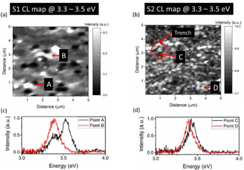
well-barrier thinning or intermixing around the V-pits and trench defects, as confirmed by RT CL
hyperspectral imaging shown in Fig. 3(a-d) (and Fig. S4 in Supplementary Material) as well as
[image:7.612.203.446.71.235.2]as shown in Fig. 3(a). We extracted the CL spectra inside (point A) and away from the V-pits
(point B). For S1, we are able to clearly resolve a high energy peak at 3.52 eV, as well as the MQW
peak at 3.38 eV, whereas we observe only the MQW peak at point B. For S2, the V-pits are less
resolvable, as shown in the CL spectra (Fig. 3(b)). However, we identify regions with (point C)
and without (point D) trench loop defects. The CL spectra show that there is no clear peak splitting
inside the trench loop of S2 (Fig. 3(d)). However, we can still observe the signature of high energy
[image:8.612.187.424.265.427.2]shift around the trench defect, compared to the trench-free part (point D).
Fig. 2. Low temperature (13 K) PL spectra of the NBE emissions of (a) S1 and (b) S2.
Fig 3. (a, b) CL hyperspectral intensity maps of S1 and S2, respectively; (c, d) CL spectra for
[image:8.612.203.446.466.636.2]To investigate the carrier dynamics, temperature-dependent PL and TRPL were studied.
Fig. 4(a) shows the temperature dependence of the PL NBE energy using pulsed laser excitation,
as it has a much higher laser power density compared to our CW laser, and can reveal the NBE
peak at higher temperatures. Both samples exhibit the known s-shape dependence of NBE energy
on temperature typical of exciton localization in III-nitride MQW structures.30-32 There is an initial
redshift in the energy peak as temperature increases from 5 K to ~60 K, indicating carrier
relocalization to lower energy states. Subsequently, a blueshift commences within the 60–110 K
temperature range. In this range, as the carriers are delocalized due to thermal activation, they are
more easily trapped by non-radiative recombination sites. Beyond 110 K, the peak energies of both
samples redshift monotonously, as predicted by Varshni.33 Furthermore, at 15 K, the NBE peaks
of both samples (3.44 eV and 3.42 eV for S1 and S2, respectively) are shifted slightly to higher
energies compared to the values obtained by CW excitation. The disparity in the results is due to
higher (~109 times) excitation power of the pulsed laser. Thus, such blueshift occurs by first
Coulomb screening of quantum-confined Stark effect (QCSE) in the MQWs, followed by the
filling of high energy band-tail states when defect states are sufficiently saturated.34,35
Fig. 4(b) shows the pulsed excitation PL spectra for both samples at 15 K. The NBE
integrated intensity of S1 is found to be ~10 times higher than that of S2 at the same excitation
power and temperature. This 10-fold increase in the integrated intensity is confirmed by PL
measurements using RT CW excitation, as shown in the inset of Fig. 3(b), whereas the yellow
Fig. 4. (a) Temperature dependence of NBE energy, (b) PL spectra at RT. (Inset: CW excitation
spectra at RT), (c) temperature dependence of IQE, and (d) PLE spectra at 550 nm of S1 and S2.
We perform PLE measurements to gain insight into the possible cause of the S1 peak
intensity increase. Fig. 4(d) shows the PLE spectra at 550 nm. The two samples have nearly
identical YL dominated by deep level defects (DLDs) in the bulk n-AlGaN layer, located at 4.2
eV (yellow shaded region). However, the YL related to the DLDs in the MQBs (blue-shaded
region, 4 eV) behaves differently. The YL of the MQBs of S2 is more prominent than that of S1.
This difference implies a higher density of defects in the MQB/MQW region of S2 compared to
S1. It has been shown that point defects, widely believed to be responsible for the YL peak in
III-nitrides, preferentially form around edge type TDs.36 This result is consistent with the RC findings.
In the light-red shaded region around 3.6 eV, which corresponds to the YL contribution from the
MQWs, the peaks are similar. However, the band edge of the MQWs of S2 is not well defined,
possibly due to the combined prominence of trench loops and V-pit defects in S2, compared to S1,
as confirmed by AFM.
We compared their relative internal quantum efficiency (IQE), η , as the ratio of the PL
[image:10.612.186.428.68.274.2]temperature (5 K) by assuming that the non-radiative channels are inactive at 5 K (in line with the
approach used in Rashba’s treatment).37-39 The IQE of S1 is found slightly higher than that of S2
in the measured temperature range. At RT, S1 had an IQE of 2.6%, whereas S2 had an IQE of
1.8%. This slight improvement in the IQE of S1 can be attributed to the lower density of edge type
dislocations, as shown in the RC results (Fig. 1(b)).
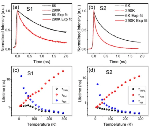
We carried out temperature-dependent TRPL measurements to further understand the
carrier dynamics of both samples. Fig. 5(a) and 5(b) show the TRPL spectra at 6 K and RT of S1
and S2, respectively. The PL decay curves of both samples are non-exponential at all temperatures.
The carrier lifetime was calculated using the method shown in Sec. 4 of Supplementary Material.
The model (solid lines in Fig. 5(a) and 5(b)) provides excellent fit to the experimental data. For
the purpose of our analyses, we used the slow decay lifetimes as the steady state PL lifetimes, to
avoid the complications caused by other fast phenomena, such as hot carrier-phonon interactions
and decay of optical phonons, which occur within the 1–100 ps range.40 The total TRPL (τTRPL)
lifetimes for S1 are 1.13 ns (6 K) and 0.62 ns (RT), whereas 0.66 ns (6 K) and 0.37 ns (RT) are
Fig. 5. RT and 6 K TRPL spectra of MQW structures of (a) S1 and (b) S2. Temperature-dependent
lifetime parameters for (c) S1 and (d) S2.
By assuming that the radiative recombination in each sample reaches maximum at low
temperature, radiative, τrad, and non-radiative, τnr recombination lifetimes are extracted.41 Fig. 5(c)
and 5(d) show the temperature dependence of τTRPL, τrad and τnr for S1 and S2, respectively. Both
samples exhibit a monotonous increase in radiative recombination across the entire temperature
range, while the non-radiative recombination rapidly decreases with increasing temperature. In
both samples, non-radiative phenomena become the dominant carrier recombination mechanism
at ~60 K, which coincides with the temperature at which the carrier delocalization process is
observed in the temperature-dependent PL in Fig. 4(a). Both the radiative carrier lifetime—τrad =
1.13 ns (6 K) and 19.78 ns (RT) — and the non-radiative carrier lifetime—τnr = 0.64 ns (RT) —of
S1 are observed to be about twice as long as those of S2—τrad =0.66 (6 K) and 11.66 ns (RT),
whereas τnr = 0.38 ns (RT). The longer τnr measured for S1 is attributed to the lesser contribution
from non-radiative effect in the recombination process,42-44 as a result of the lower density of
defects in S1 (consistent with our PLE and RC results). However, S1 has longer τrad relative to S2,
the strain relaxation. As was previously discussed, the III-nitride layers overgrown on 201
-oriented Ga2O3 (S1) have been shown to be more strain relaxed than those grown on Al2O3. While
this can lead to low rates of radiative recombination processes (longer τrad),45 the decline in overlap
probability can effectively be offset by the higher crystalline quality of the overgrown layer,
leading to better optical performance.46
In conclusion, GaN/AlGaN MQWs were grown on 201 -oriented β-Ga2O3 substrate.
Structural and optical analyses revealed that, in the absence of enhanced growth techniques, a
generally higher structural and optical quality of MQW growth was achieved on 201 -oriented
β-Ga2O3 when compared to a similar structure grown on Al2O3 substrate. Carrier lifetime analyses
confirmed that the density of non-radiative recombination centers in MQWs grown on 201
-oriented β-Ga2O3 was lower compared to that in MQWs grown on Al2O3. Thus, under
systematically optimized conditions, growth of highly efficient vertical UV emitting devices based
on III-nitrides (including VCSELs) on β-Ga2O3 substrates should be possible, allowing for device
designs that would benefit from the transparent and conductive properties of β-Ga2O3.
Supplementary material
See supplementary material for defect density estimation methods, STEM and CL images
confirming well/barrier thinning and intermixing as well as the method employed when calculating
carrier lifetimes.
Acknowledgements
References
1 S. D. Lester, F. A. Ponce, M. G. Craford, and D. A. Steigerwald, Appl. Phys. Lett. 66, 1249
(1995).
2 S. A. Kukushkin, A. V. Osipov, V. N. Bessolov, B. K. Medvedev, V. K. Nevolin, and K.
A. Tcarik, Rev. adv. mater. sci. 17, 1 (2008).
3 M. M. Muhammed, M. Peres, Y. Yamashita, Y. Morishima, S. Sato, N. Franco, K. Lorenz,
A. Kuramata, and I. S. Roqan, Appl. Phys. Lett. 105, 042112 (2014).
4 M. M. Muhammed, M. A. Roldan, Y. Yamashita, S. L. Sahonta, I. A. Ajia, K. Iizuka, A.
Kuramata, C. J. Humphreys, and I. S. Roqan, Sci. Rep. 6, 29747 (2016).
5 Z. Hajnal, J. Miró, G. Kiss, F. Réti, P. Deák, R. C. Herndon, and J. M. Kuperberg, J. Appl.
Phys. 86, 3792 (1999).
6 H. Murakami, K. Nomura, K. Goto, K. Sasaki, K. Kawara, Q. T. Thieu, R. Togashi, Y.
Kumagai, M. Higashiwaki, A. Kuramata, S. Yamakoshi, B. Monemar, and A. Koukitu, Appl. Phys. Express 8, 015503 (2015).
7 W. Mi, X. Du, C. Luan, H. Xiao, and J. Ma, RSC Adv. 4, 30579 (2014). 8 S. Kim, J. E. Spanier, and I. P. Herman, Jpn. J. Appl. Phys. 39, 5875 (2000).
9 V. N. Maslov, V. M. Krymov, M. N. Blashenkov, A. A. Golovatenko, and V. I. Nikolaev,
Tech. Phys. Lett. 40, 303 (2014).
10 J. Zhang, C. Xia, Q. Deng, W. Xu, H. Shi, F. Wu, and J. Xu, J. Phys. Chem. Solids 67,
1656 (2006).
11 K. Gurnett and T. Adams, III-Vs Review 19, 39 (2006).
12 H. Aida, K. Nishiguchi, H. Takeda, N. Aota, K. Sunakawa, and Y. Yaguchi, Jpn. J. Appl.
Phys. 47 (11R), 8506 (2008).
13 K. Shimamura, E. G. Víllora, K. Domen, K. Yui, K. Aoki, and N. Ichinose, Jpn. J. Appl.
Phys. 44, L7 (2005).
14 E. G. Villora, S. Arjoca, K. Shimamura, D. Inomata, and K. Aoki, Proc. SPIE 8987,
Oxide-based Materials and Devices V, 89871U (2014).
15 E. G. Víllora, K. Shimamura, K. Kitamura, K. Aoki, and T. Ujiie, Appl. Phys. Lett. 90,
234102 (2007).
16 S. Ito, K. Takeda, K. Nagata, H. Aoshima, K. Takehara, M. Iwaya, T. Takeuchi, S.
Kamiyama, I. Akasaki, and H. Amano, Phys. Stat. Sol. (c) 9, 519 (2012).
17 M. M. Muhammed, N. Alwadai, S. Lopatin, A. Kuramata, and I. S. Roqan, ACS. Appl.
Mater. Inter. 9, 34057 (2017).
18 Y. J. Sun, O. Brandt, T. Y. Liu, A. Trampert, K. H. Ploog, J. Bläsing, and A. Krost, Appl.
Phys. Lett. 81, 4928 (2002).
19 J. Bruckbauer, P. R. Edwards, T. Wang, and R. W. Martin, Appl. Phys. Lett. 98, 141908
(2011).
20 F. C.-P. Massabuau, S.-L. Sahonta, L. Trinh-Xuan, S. Rhode, T. J. Puchtler, M. J. Kappers,
C. J. Humphreys, and R. A. Oliver, Appl. Phys. Lett. 101, 212107 (2012).
21 X. Li, S. Sundaram, P. Disseix, G. Le Gac, S. Bouchoule, G. Patriarche, F. Réveret, J.
Leymarie, Y. El Gmili, T. Moudakir, F. Genty, J. P. Salvestrini, R. D. Dupuis, P. L. Voss, and A. Ougazzaden, Opt. Mater. Express 5, 380 (2015).
22 I.-H. Kim, H.-S. Park, Y.-J. Park, and T. Kim, Appl. Phys. Lett. 73, 1634 (1998).
23 K. S. Son, D. G. Kim, H. K. Cho, K. Lee, S. Kim, and K. Park, J. Cryst. Growth 261, 50
24 J. Bruckbauer, P. R. Edwards, S.-L. Sahonta, F. C. P. Massabuau, M. J. Kappers, C. J.
Humphreys, R. A. Oliver, and R. W. Martin, J. Phys. D: Appl. Phys. 47, 135107 (2014).
25 J. Smalc-Koziorowska, E. Grzanka, R. Czernecki, D. Schiavon, and M. Leszczyński, Appl.
Phys. Lett. 106, 101905 (2015).
26 F. C. P. Massabuau, C. C. Tartan, R. Traynier, W. E. Blenkhorn, M. J. Kappers, P. Dawson,
C. J. Humphreys, and R. A. Oliver, J. Cryst. Growth 386, 88 (2014).
27 J. H. Son and J. L. Lee, Opt. Express 18, 5466 (2010).
28 M. A. Reshchikov and H. Morkoç, J. Appl. Phys. 97, 061301 (2005).
29 A. Ben Slimane, A. Najar, R. Elafandy, D. P. San-Román-Alerigi, D. Anjum, T. K. Ng,
and B. S. Ooi, Nanoscale Res. Lett. 8, 342 (2013).
30 A. Yasan, R. McClintock, K. Mayes, D. H. Kim, P. Kung, and M. Razeghi, Appl. Phys.
Lett. 83, 4083 (2003).
31 K. B. Lee, P. J. Parbrook, T. Wang, F. Ranalli, T. Martin, R. S. Balmer, and D. J. Wallis,
J. Appl. Phys. 101, 053513 (2007).
32 I. A. Ajia, P. R. Edwards, Z. Liu, J. C. Yan, R. W. Martin, and I. S. Roqan, Appl. Phys.
Lett. 105, 122111 (2014).
33 Y. P. Varshni, Physica 34, 149 (1967).
34 J. Zhang and N. Tansu, J. Appl. Phys. 110, 113110 (2011).
35 H. Wang, Z. Ji, S. Qu, G. Wang, Y. Jiang, B. Liu, X. Xu, and H. Mino, Opt. Express 20,
3932 (2012).
36 J. Elsner, R. Jones, M. I. Heggie, P. K. Sitch, M. Haugk, Th Frauenheim, S. Öberg, and P.
R. Briddon, Phys. Rev. B 58, 12571 (1998).
37 D. Iida, A. Fadil, Y. Chen, Y. Ou, O. Kopylov, M. Iwaya, T. Takeuchi, S. Kamiyama, I.
Akasaki, and H. Ou, AIP Adv. 5, 097169 (2015).
38 T. Kohno, Y. Sudo, M. Yamauchi, K. Mitsui, H. Kudo, H. Okagawa, and Y. Yamada, Jpn.
J. Appl. Phys. 51 (7R), 072102 (2012).
39 O. Brandt, J. Ringling, K. H. Ploog, H. J. Wunsche, and F. Henneberger, Phys. Rev. B 58,
15977 (1998).
40 J. Shah and Lucent Technologies (Firm), Ultrafast spectroscopy of semiconductors and
semiconductor nanostructures, 2nd enl. ed. (Springer Verlag, Berlin; New York, 1999), pp.xvi.
41 T. Li, A. M. Fischer, Q. Y. Wei, F. A. Ponce, T. Detchprohm, and C. Wetzel, Appl. Phys.
Lett. 96, 031906 (2010).
42 J. Dekker, A. Tukiainen, N. Xiang, S. Orsila, M. Saarinen, M. Toivonen, M. Pessa, N.
Tkachenko, and H. Lemmetyinen, J. Appl. Phys. 86, 3709 (1999).
43 V. Liuolia, A. Pinos, S. Marcinkevičius, Y. D. Lin, H. Ohta, S. P. DenBaars, and S.
Nakamura, Appl. Phys. Lett. 97, 151106 (2010).
44 Y. Li, D. P. Byrnes, and E. B. Stokes, ECS J. Solid State Sci. Technol. 2, R267 (2013). 45 C. Du, X. Huang, C. Jiang, X. Pu, Z. Zhao, L. Jing, W. Hu, and Z. L. Wang, Sci. Rep. 6,
37132 (2016).
46 S. A. Al Muyeed, W. Sun, X. L. Wei, R. B. Song, D. D. Koleske, N. Tansu, and J. J. Wierer,