Abstract: In this nano technical world the “Complementary MOS technology” can be replaced by using “Quantum Dot Cellular Automata” with reversible logical phenomenon to achieve a fault tolerant, low-cost nano electronics formation by feature size, latency and power consumption minimization. The memory is one of the most interesting part of research in this digital world. This paper represents an optimizing high-frequency (in THz) reversible design of a “Random Access Memory” which is simulated by using nano electronics ‘QCA’ simulator to get a better performance than “Complementary MOS technology” with high frequency (in THz), less occupied area and dissipated power. This paper also shows a highly-flexible magnetic quantum cell logic-design and MTJ logical representation which is used for non-volatile MRAM which is widely used in digital electronics world and as a part of aerospace and military device. A reversible nano electronics formation of the control logic to select the word-line and input-line of the MRAM also presented here. The reversible-logic can avoid the information-loss in memory device by zero-heating technique. Non-reversible formations dissipate ‘KTln2’ energy per bit which can be ignored in reversible formation. But, read disturb at low write current is a major issue of MTJ MRAM due to the same path of read/write current path. In this paper a three dimension reversible “Read Disturb Detection Circuit” is formed by nano electronics ‘QCA’ technology which bit-wise follows the control logic of read-disturb-detection technique and the same figure also simulated by ‘VHDL’ coding in Xilinx software to prove the advantages of ‘QCA’ technology contrast to Xilinx This paper also focuses on the correspondence between change of temperature and supply power.
Keywords :Magnetic Tunnel Junction, Quantum cell, Reversible Logic, Read Disturb Detection.
I. INTRODUCTION
QCA or Quantum Dot cellular Automata are used to replace the CMOS technology in a proper alternative method because of its faster switching possibility, less area, higher clock-frequency (in THz) and low power-consumption and we can access more bits in a single time
Revised Manuscript Received on December 05, 2019.
Rupsa Roy*, ETCE. Jakir Hossain Institute of Polytechnic, Murshidabad, W.B, India.
Swarup Sarkar, EC department, Sikkim Manipal University, Sikkim, India.
Sudipta Das, Department of ECE, IMPS College of Engineering & Technology, Malda, W.B, India.
by applying QCA technology compare to CMOS technology [1]. A portable high speed reversible memory formation with less heat dissipation and occupied area is introduced in this paper.Reversible Devices should be logically and physically reversible by making the input and outputs uniquely recoverable from each other and can be properly run in backward direction respectively [2]. We can realize arbitrary functions (non-symmetric) using repeated variables.Due to the high leakage problem and also the scalability problem the SRAM, DRAM are replaced by nonvolatile Magneto resistive RAM with spin transfer torque technique to get more flexibility, low power dissipation, more endurance, more speed and less occupied area. MRAM stores data (using electric charge) in magnetic region with uniform magnetization. In the Spintronic technique a torque is applied to the chargeable-layer by the spin of electron flow and this phenomena takes place in a magnetic tunnel junction (‘MTJ’) which mainly works for electron-tunneling and this is a quantum-phenomena. In this magnetic process the memory uses a pair of ‘ferromagnetic metal plates’ and a thin layer of an insulating-material separates them and the orientation of the plates (parallel or not) is determined by ‘1’ and ‘0’ binary bits. MTJ MRAM faces some challenges. Mainly it faces problems due to read disturb at low current [3]. This paper presents a multiple layer or 3-D reversible MTJ or magnetic tunnel junction structure by ‘QCA’ technology which bit-wise follows the control logic of Spintronic process with the application of the “read disturb detection technique”.
II. BACKGROUND
This paper presents the applied cell-design of QCA (fig.1), the different cell designs (fig.2) and the different wiring process of QCA (fig.3 and fig.4). This paper also presents the simulator-parameters in table.1.
Fig.1. A cell-design of QCA
A Multilayer High-Speed
Magnetic-Tunnel-Junction Magneto-resistive RAM Structure with
Read-Disturb-Detection Circuit by Using
Nano-Electronics Quantum Dot Cellular Method
Fig.2. 90-degree wire structure (upper part) and 45-degree wire structure (lower part) of a QCA-cell.
Fig.3. Wiring process of 90-degree (upper part) and 45-degree (lower part) quantum cell.
Basic reversible gates [4] (Reversible-NOT and F-Gate) and ‘five input’ majority gates are used in this paper to design reversible RAM and MRAM formation. The equation of applied ‘five input’ majority gate is:
M (A, 1, B, C, D) =A (B+C+D) +BC+BD+CD
Table- I: Table of simulation-parameters [2019]
Parameters are used Values of the parameters
Cell-Size 324 nm2
Distance between layers 11.5 nm
Dot-Diameter 5 nm
Clock-Area (lower) 3.800000e-023
Clock-Area (Upper) 9.800000e-022
Area of clock-shift 0
Clock-Amplitude-Factor 2
Permittivity (relative) 12.90
Sample-Numbers 50,000
Convergence-tolerance 0.001
Maximum interaction of one sample
100
III. RELATEDWORKS
Some related works in 2018-19 are summarized in this part. In paper [5] an SOC feature was presented using 180 nm CMOS/200 nm MTJ MRAM and required area, time and energy of this design was 23 mm2, 4.15 ns and 98.7 no respectively. In the paper [6] “1 Mb pe STT-MRAM” was
designed using “28 nm FD-SOI-CMOS” technology and here the write latency was 10 ns and required energy 3pJ. Paper [7] has given a brief discussion about the “MgO-based MTJ” materials and in paper [8] a “1T1R STT MRAM” was designed using “28 nm” technology with 0.214 mm2 area, 20 ns writing speed and 3.6 mW power consumption. The operation of MTJ was represented through Boolean function in the paper [9] using “HieIM” with 21.8 μm2
area and 3.2 no energy. Here 1620 cycles (delay) required to access the data. Three different designs of MRAM such as “STT MRAM”, “SOT MRAM” and “VC MRAM” have been compared in paper [10] and presented that the “STT MRAM” gives best solution to reduce the area (70-100 F2 cell-size), delay and power consumption. Paper [11] presented a “512 KB STT MRAM” cache memory using 20 nm technology node. The ‘SNR’ value of “STT MRAM” (6 dB - 16 dB) was given in paper [12] and paper [13] presented the stiffness constant of “MRAM” (26.6 pJ/m for 425°C temperature) using “MgO / Fecal based MTJ”. Paper [14] calculated the size of heat-effect of Spintronic-device which was 300 n J/ Vm and the stability-factor was above 60 of the same technology [15]. The paper [16] accorded the same stability of “STT MRAM” for 4 nm diameter and 300 K temperature using “10 nm” node. The “pMTJ MRAM” design was formed in [17] where 66% TMR was changed.“MRAM” using “22 FFL FinFET Technology” was designed in paper [18] for high quality performance and it can work -40°C to 125°C temperature range with 0.048 µm2 area and the required time (8ns for 0.6 V) was given in paper [19]. A “Quad Interface MTJ” was designed in [20] using “1-X” technology by applying an extra MgO layer (90 nm diameter) for getting low power-consumption. In the paper [21] the MTJs were integrated with CMOS for high-density (over 100 Mb) Spintronic (“STT”) memory-design. A “6T-STT MRAM” with 400 mW powers and 45 ns delay was formed in the paper [22] using “500 x” performance for 1 GB density and [23] presented an “MRAM” with 50 nm diameter. [24] applied a fast “gem 5” simulation on “MRAM” and “DRAM” and manifested that we can replace the other
memories using magnetic-RAM to reduce power
consumption up to ‘8%’ and ‘27%’ at the cost of ‘2x’ the area with 10.4 ns time-delay.
IV. THEPROPOSEDMETHOD
Fig. 4. Schematic Diagram of Memory Cell [25].
Fig.5. Irreversible QCA Design of RAM [25].
Fig.6. Proposed Reversible Random Access Memory.
The same logic-design is simulated through ‘VHDL’ code in ‘Xilinx’ and the compared outcomes are enlisted in table-II. Today’s world is widely using ‘MTJ MRAM’ technology which is a modern replacement of other RAM-cells. The logical representation of magnetic cells can be formed by using a three-input majority gate and an inverter gate one after another [27] and if the three input majority gate is replaced by a five input majority, the previous structure works as a “XOR / XNOR” MTJ logic circuit. This paper suggests a reversible control circuit of word-line and input-line selection of magneto resistive RAM structure, which is formed by QCA technology (fig. 7). In fig. 7 the three inputs A, B and C presents the word-line, select-line and input-line respectively. If the A is one and Bit zero then output Q read the same bit pattern of C and if A is one and Bit also one then the Q presents inverting
output of C. In this figure the Q’ gives the ‘XOR’ output of B and C and Q’’ is the representation of input A.
Fig.7. Reversible control circuit of MRAM.
[image:3.595.310.541.76.233.2]The write-current of “STT MRAM” is 5 to 10 times higher than the read-current. So, at the time of read to write (when a flip of ‘bit’ cell is required) the magnetic disturbances in ‘MTJ’ take place. This is the main reason of read-disturb in ‘MRAM’. This paper presents a three dimension reversible read disturb detection control circuit by using quantum-cells and the same figure also deigned through ‘VHDL’ coding in ‘Xilinx’ and the advancement of ‘QCA’ technology contrast to ‘Xilinx’.
Table- II: Compared outcomes between ‘Xilinx’ and ‘QCA Designer’.
Outcomes In ‘Xilinx’ In ‘QCA Designer’
Area 25 IOB 0.036 µm2
Latency 8.752 ns 1 clock-cycle
Power 0.204 W 0.03 W for 0.7 Ek
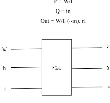
This paper shows the block-representation of F-Gate which is applied as a reversible gate in this design in fig. 8, where
P = W/l Q = in
[image:3.595.61.287.366.551.2]Out = W/l. (~in). rl
Fig.8. Reversible F-Gate.
The circuit-design of control-logic of MTJ with read-disturb-detection process and
[image:3.595.305.545.394.475.2] [image:3.595.317.508.520.698.2]here in fig. 9 and table- III respectively.
Fig.9. Circuit-Diagram of control logic of read-disturb-detection [3].
Table- III: Truth-table of control logic of MTJ with read-disturb-detection [3].
The normal reversible formation (required 2 clock-zones) and multilayer or 3-D formation (required 1 clock-zone) of the above circuit and also the inverting-outcomes are proposed in this paper which are presented in fig. 10, 11, 12 and 13 respectively and the ‘RTL’ and ‘Technology’ schematic of the above figure (synthesized in ‘Xilinx’) are presented in fig.14 and 15 respectively. The schematic figures properly shoes the logical representation of the proposed ‘MTJ’ design and the logic-diagrams, truth-tables and k-map of different circuits which are used in this proposed ‘MTJ’ circuit can be obtained by the technology schematic.
Fig.10. Reversible formation of MTJ control logic with read-disturb-detection using ‘QCA’.
Fig.11. 3-D Reversible formation of MTJ control logic with read-disturb-detection using ‘QCA’.
Fig.12. Reversible formation of control logic of MTJ with read-disturb-detection and inverting output using
‘QCA’.
Fig.13. 3-D Reversible formation of control logic of MTJ with read-disturb-detection and inverting output using
Fig.14. ‘RTL’ Schematic of MTJ control logic with read-disturb-detection using ‘Xilinx’.
Fig.15. ‘Technology’ Schematic of MTJ control logic with read-disturb-detection using ‘Xilinx’.
V. SIMULATIONRESULTSANDCOMPARISON
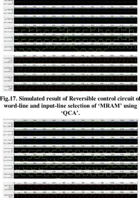
[image:5.595.312.541.49.210.2]The simulated result of reversible ‘RAM’ and the reversible control circuit of word line and input line selection of magneto resistive random access memory are presented in fig. 16 and fig. 17 respectively. The outcomes of fig. 17 follows table IV. This research work also shows the outcome of simulated 3-D reversible read-disturb-detection circuit of ‘STT MRAM’ formed by ‘QCA’ technology with and without changing the clock-zone in fig. 18 and 19 respectively.
[image:5.595.309.543.57.388.2]Fig.16. Simulated result of Reversible ‘RAM’ using ‘QCA’.
Fig.17. Simulated result of Reversible control circuit of word-line and input-line selection of ‘MRAM’ using
‘QCA’.
[image:5.595.310.540.204.420.2]Fig.18. Simulated Result of 3-D Reversible control logic of MTJ with read-disturb-detection using ‘QCA’.
Fig.19. Simulated Result of Reversible control logic of MTJ with read-disturb-detection using ‘QCA’ without
changing the clock-zone.
Table- V represents the compared outcomes of different proposed structures formed in different technology such as,
“45 nm CMOS Technology”(2018), “28 nm
[image:5.595.55.283.252.401.2] [image:5.595.55.283.582.746.2]Table- IV: The bit-wise representation of proposed reversible control circuit of MRAM
Table-V: Table of compared outcomes of different proposed structures formed in different technology
Word line Select line Input line Q’’ = Word line Q’ = XOR (Select line and Input line)
Q = Q’ AND Word line
1 0 0 1 0 0
1 0 1 1 1 1
1 1 0 1 1 1
1 1 1 1 0 0
Fig.20. Graph of ambient temperature vs. power consumption.
Fig.21. Pie-Chart of junction temperature (0°C - 110°C) vs. supply power.
VI. CONCLUSION
The new designs of reversible ‘RAM’ and multilayer reversible control logic of ‘MTJ’ (in ‘STT MRAM’) with ‘read-disturb-detection’ process is presented in our paper by using ‘QCA-designer’. These proposed formations give better response to reduce the number of required cells, area (0.01 µm2), delay (0.5 clock cycles) and power (0.008 µW) than other previously suggested designs and also this paper presents a comparison of area, delay, power with reversibility process between the circuits formed by ‘QCA-designer’ and the same circuits implemented through ‘Xilinx’ software (using ‘VHDL’ code). This paper also shows the relation between ambient temperature and power consumption and between junction temperature and supply power through graph and pie-chart. The exponential increment of the total power of the suggested device with the room-temperature increment are clearly represented here through a graphical representation and it is also shows that after “80 degree C” the increment of power with the increment of room-temperature is stopped.In future we can try to reduce the area, energy and number of the garbage-outputs by reducing the cell-size, dot-diameter and by applying new reversible-gates of the proposed figures and also we can try to improve the fault tolerance and reversibility of the formations. This proposed design is required to fabricate for hardware implementation which is required for proper real-world application.
REFERENCES
1. Farah Sharman, Md. Masbaul Alam Polash, Md. Shamsujjoha, Lafifa Jamal, Hafiz Md. Hasan Babu, “Design of a Compact Reversible Random Access Memory”, ICCSIT, IEEE, June 2011, Vol. 978, no. 1, pp. 61284-836-5.
2. B. Raghu Kant, B. Murali Krishna, M. Shridhar, V. G. Santhi
Swaroop, “A Distinguish between Reversible and Conventional logic Gates,” IJERA, Mar-Apr 2012, Vol. 2, no. 2, pp. 148-151.
3. Rajendra Bishnoi, Mojtaba Ebrahimi Fabian, Oboril Mehdi B.Tahoori, “Read Disturb Fault Detection in STT-MRAM.”, 3rd INTERNATIONAL TEST CONFERENCE, IEEE, 2014.
4. Mostafa Abdollahian Dehkordi, Abbas Shahini Shamsabadi, Behrouz Shahgholi Ghahfarokhi, Abbas Vafaei , “Novel RAM cell designs based on inherent capabilities of quantum-dotcellular automata”, Microelectronics Journal, 2014, Vol.42, pp. 701-708.
5. Sophiane Senni, Frederic Ouattara, Jad Modad, Kaan Sevin,
Guillaume Patrigeon, Pascal Benoit, Pascal Nouet, Lionel Torres , “From Spintronic Devices to Hybrid CMOS/Magnetic System On Chip”, IEEE , 2018,
6. Guillaume Patrigeon, Pascal Benoit, Lionel Torres, Sophiane Senni,
Guillaume Prenat, Gregory Di Pendina, “Design and Evaluation of a 28-nm FD-SOI STT-MRAM for Ultra-Low Power microcontrollers”, IEEE Access,IEEE, In press, 2019, Vol. 7, pp.58085-58093.
7. Dmytro Apalkov, Bernard Dieny, J. Slaughter, “Magneto resistive
Random Access Memory”, Pro_x0002_ceedings of the IEEE, Institute of Electrical and Electronics Engineers, 2016, Vol. 104, pp.1796 - 1830.
8. Qing Dong, Zhehong Wang, Jongyup Lim, Yiqun Zhang, Yi-Chun
Shih, Yu-Der Chih, Jonathan Chang, David Blaauw, Dennis Sylvester, “A 1Mb 28nm STT-MRAM with 2.8ns Read Access Time at 1.2V VDD Using Single-Cap Offset-Cancelled Sense Amplifier and In-situ Self-Write-Termination”, ISSCC 2018, SESSION 30, EMERGING MEMORIES, 30.2.
9. Farhana Parveen, Zhezhi He, Shaahin Angizi, Deliang Fan, “HieIM:
Highly Flexible In-Memory Computing using STT MRAM”. IEEE, 2018, Vol. 978, no.1, pp. 5090-0602.
10. Tetsuo Endoh and Hiroaki Honjo, “A Recent Progress of Spintronics
Devices for Integrated Circuit Applications”, J. Low Power Electron. Appl. 2018, Vol. 8, pp. 44.
Designs Area Delay Leakage
Power
“45 nm CMOS” (2018)
5.871 mm2 1.93 ns 730 mW
“28 nm FDSOI”
(2019)
0.036 µm2 10 ns (100 MHz max)
352 µW
“Xilinx” 6 IOB 6.236 ns 203 mW
“QCA
11. Esteban Garzon, Macro Lanuza, “Assesment of STT MRAM performance at nanoscaled technology nodes using device-to-memory simulation framework,” Microelectronic Engineering, Vol. 215, July 2019, 111009.
12. A. Vedyayev, N. Ryzhanova, N. Strelkov, T. Andrianov, A. Lobachev,
et al, “Non-local signal and noise in T-shape lateral spin-valve structures”, Physical Review Applied, American Physical Society, 2018, Vol. 10.
13. Jyotirmoy Chatterjee, Eric Gautier, Marc Veillerot, Ricardo Sousa,
Stéphane Auffret, et al, “Physicochemical origin of improvement of magnetic and transport properties of STT-MRAM cells using Tungsten on Fe CoB storage layer”, Applied Physics Letters, American Institute of Physics, In press, 2019, Vol. 114, pp.092407.
14. Osaka University, “Novel technology reduces energy consumption of
MRAM and AI hardware”, phys.org, January, 2019.
15. Steven Lequeux, V. Nguyen, N. Perrissin, J Chatterjee, L. Tille, et al.,
“Towards high density STT_x0002_MRAM at sub-20nm nodes”, 29th Magnetic Recording Conference, Aug 2018.
16. Nicolas Perrissin, Steven Lequeux, Nikita Strelkov, Antoine Chavent,
Laurent Vila, et al., “A highly thermally stable sub-20 nm magnetic random-access memory based on perpendicular shape anisotropy’, Nanoscale, Royal Society of Chemistry, 2018, Vol. 10, no. 25, pp.12187.
17. N. Strelkov, A. Chavent, A. Timopheev, R. Sousa, I. Prejbeanu, et al,
“Impact of Joule heating on the stability phase diagrams of perpendicular magnetic tunnel junctions”, Physical Review B : Con_x0002_densed matter and materials physics, American Physical Society, 2018,Vol. 98, pp.214410.
18. O. Golonzka et al., "MRAM as Embedded Non-Volatile Memory
Solution for 22FFL FinFET Technology," IEEE International Electron Devices Meeting (IEDM), San Francisco, CA, 2018, Vol. 18, no. 1, pp. 1-4.
19. J. A. O'Donnell et al., "eNVM MRAM Retention Reliability Modeling
in 22FFL FinFET Technology," IEEE International Reliability Physics Symposium (IRPS), 2019, Monterey, CA, USA, 2019, pp. 1-3.
20. K.Nishioka, H.Honjo, S. Ikeda, et.al, “Development of durable MTJ
under harsh environment for STT-MRAM at 1Xnm technology node,” PHYS.ORG, June 2019, pp. 1-3.
21. K.Nishioka, H.Honjo, S. Ikeda, et.al “Researchers develop 128Mb
STT-MRAM with world's fastest write speed for embedded memory”, PHYS.ORG, December 28.
22. Turbo majumder, Manan Suri, Vinay shekhar, “NoC Router Using
STT-MRAM Based Hybrid Buffers with Error Correction Limited Flit Retransmission,” IEEE, 2015, Vol. 978, no. 1, pp. 4799-8391.
23. Runzi Hao, Lei Wang, Tai Min. A Novel, “STT-MRAM Design With
Electric-Field-Assisted Synthetic Anti-Ferromagnetic Free Layer”, IEEE TRANSACTIONS ON MAGNETICS, VOL. 55, NO. 3, March 2019.
24. Manu Komalan, Oh Hyung Rock, Matthias Hartmann, Sushil Sakhare,
Christian Tenllado, Jose Ignacio G ´ omez ´, Gouri Sankar Kar, Arnaud Furnemont, Francky Catthoor, Sophiane Senni, David Novo, Abdoulaye Gamatie and Lionel Torres, “Main memory organization trade-offs with DRAM and STT-MRAM options based on gem5-NVMain simulation frameworks”, EDAA, March 2018, Vol. 978, no. 3, pp. 9819263.
25. Javad Chaharlang, Mohammad Mosleh, “An Overview on RAM Memories in QCA Technology.”,Majlesi Journal of Electrical Engineering, Vol. 11, No. 2, June 2017.
26. Navid Farazmand, Masoud Zamaniand Mehdi B. Tahoori, “Online
Fault Testing of Reversible Logic UsingDual Rail Coding”, IEEE, 2014, Vol. 978, no. 1, pp. 4244-7723.
27. Liuyang Zhang, Wang Kang, Hao Cai, Peng Ouyang, Lionel Torres,
Youguang Zhang, Aida Todri Sanial, Weisheng Zhao, “A Robust Dual Reference Computing-in-Memory Implementation and Design Space Exploration within STT-MRAM,” IEEE, Computer Society, July 2018, pp. 275-280.
28. A. Orlov, A. Imre, G. Csaba, L. Ji, W. Porod, G. H. Bernstein,
“Magnetic Quantum-Dot Cellular Automata: Recent Developments and Prospects,” Journal of Nanoelectronics and Optoelectronics, ASP, 2008, vol. 3, pp. 1-14.
AUTHORSPROFILE
Rupsa Roy Is working as a lecturer in Jakir Hossain Institute of Polytechnic (JHIP) in West Bengal. She has applied her M.TECH degree in VLSI and Embedded System from Kalinga Institute of industrial Technology (KIIT, Bhubaneswar) in the year 2018 and B.Tech degree in Applied Electronics and Instrumentation from Future Institute of Engineering and Management under MaulanaAbulKalam Azad University of Technology, West Bengal (M.A.K.A.U.T, W.B) in the year 2015. She has one published paper in an International journal and one IEEE Conference Paper on Double-gate MOSFET.
Prof (Dr) Swarup Sarkar is a well-known Professor in the field of VLSI design and micro chip design. He is working as a professor in Sikkim Manipal University, Sikkim, India. Dr. Swarup Sarkar has received his PhD in VLSI µ chip design from NIT, Durgapur, India. Dr. Sarkar is the author of 48 reputed international journal and 3 books. He also invited chair speaker of international Gene convention.