Abstract: This paper proposes amodified SEPIC converter in coupled inductor based high gain dc-dc converter. The proposed topology presents low switch voltage and high efficiency for low input voltage, low ripple current and high output voltage applications. Two alternatives with and without magnetic coupling are analyzed. The magnetic coupling allows increasing the static gain with a reduced switch voltage. The theoretical analysis and experimental results are presented. The efficiency obtained with the prototype without magnetic coupling was 81%, 83.2%.With magnetic coupling85.5% was improved to nominal output power. Efficiency equal to 85% was obtained with the prototype model.
Keywords: Multi-Converter System, Single-Ended Primary Inductance Converter (SEPIC).Coupled inductor, Pulse width modulation (PWM).
I. INTRODUCTION
The innovation used to pack the parts of the utilization of hysteretic controllers for low voltage controllers utilized in PC and communication frameworks due its different focal points. Favourable circumstances of this control approach incorporates quick reaction and vigorous with basic plan and usage. They don't require segments for feedback loop pay [1]-[3]. This diminishes the quantity of parts and size of hypothetical examination for usage and furthermore decreases the structure exertion for figuring the circuit segment esteems (like inductor, capacitor, and information voltage). They reaction to aggravations and load change directly after the transient happens. Consequently they give fantastic transient exhibitions.
Zero voltage switching plans have been referred to for quite a while as a straightforward and viable method for executing current control of switching converters. Variable switching recurrence, solid load reliance of the normal switching recurrence, and the conceivable outcomes for limit cycle activity with high recurrence switching, are notable disservices of essential hysteresis controllers. All things considered, ZVS and ZCS plans can be significant for some applications, because of the quick powerful execution that is exceedingly robust concerning changes in frameworks parameters and working conditions [4]-[6].
Revised Manuscript Received on March 08, 2019.
Naresh.C, Assistant Professor, St. Joseph‘s Institute of Technology, Chennai, India,
Karthikeyan. R, Associate Professor, Sri Venkateswara College of Engineering, Sriperumbudur, Chennai, India.
Switching-transistors are driven by a duty-cycle that is relative to the control-voltage. This strategy is proportionate to VMC(voltage-mode-control) and it utilizes the control voltage which is a distinction of genuine yield voltage and a reference picked. This creates the pulse-train used to drive the switches. Another strategy known as pulse-mode-control is utilized where the pinnacle current of the inductor is utilized as a control method. Every one of these procedures has its own points of interest and burdens. The prior types of Bang-bang-controllers have been rethought by specialists because of its favourable circumstances of quick transient reaction and less misfortunes and a lesser segment tally seen by power-electronic-scientist [7].
A SEPIC converter is generally encompassed the finest power feature rectification presentation, but the effectiveness is not equivalent to the further explanation. A fly back converter is not containing a transformer and the related leakage ring consequence [8].Also, it is premeditated for a broad variety of output and input proportion. In DCM, the input inductor current is maintained the input voltage through lesser ripple current when contrasted by the flyback and boost converters [9]. Here, the isolated SEPIC converter employs a transformer for to restore the second inductor [10]. The two magnetic elements actually augment the expenditure among one magnetic core. The symmetrical and asymmetrical half-bridge converters are employs for standard power applications [11]. These converters are generally included enhanced power feature and enhanced effectiveness among two switches. Besides, the transformer is executed in two quadrants through the additional exploitation of core and lesser size of magnetic elements for both the transformer and output inductor [12] [13]. The foremost benefit of SEPIC converter is that it encompassing a low input current ripple. On the other hand, a mass inductor is employed to diminish the current ripple [14]. Input current ripple is considered as a significant necessity for the broad employ of low voltage resources like batteries, supercapacitors, and fuel cells [15] [16].
II. SIMULATION RESULTS
Case1:
SEPIC-Based High Step-Up DC/DC Converter
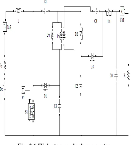
Fig. 2.1 High step up dc-dc converter
[image:2.595.60.283.65.311.2]The DC input voltage is revealed in Fig 2.2.The current through the inductor L is revealed in Fig 2.3. The switching pulse given to the gate and the drain current and the voltage across the switch S1 is revealed in Fig 2.4.
Fig. 2.2 Dc input voltage
Fig. 2.3 Current through inductor
Fig. 2.4 Gate pulse, drain Current and voltage across switch S1
[image:2.595.312.541.331.458.2]The current through the coupled inductor L1 and L2 is revealed in the Fig 2.5.The output voltage and output power for SEPIC based high step-up DC-DC converter are shown in the Fig 2.6 and Fig 2.7 respectively.
[image:2.595.304.546.342.832.2]Fig 2.5 Current through coupled inductor
Fig. 2.6 Output voltage
[image:2.595.65.271.384.714.2]Fig. 2.8 Input voltage vs Output voltage
[image:3.595.321.534.51.189.2]The graph for the input voltage and the output voltage for the SEPIC based high step-up DC-DC converter is revealed in Fig 2.8.
Fig. 2.9 Input voltage vs Output power
[image:3.595.321.528.236.632.2]The graph for the input voltage and the output power for the SEPIC based high step-up DC-DC converter are revealed in Fig 2.9.
Fig. 2.10 Input voltage vs Efficiency
The graph for the input voltage and the efficiency for the SEPIC based high step-up DC-DC converter are revealed in Fig 2.10.
Case2:
Zero-Ripple Input-Current High-Step-Up Boost–SEPIC DC–DC Converter
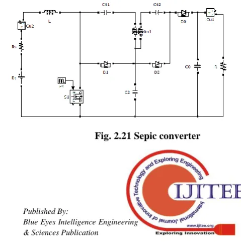
The ripple free input current with high step-up boost SEPIC DC-DC converter is simulated using the blocks of Simulink. The circuit diagram for ripple free input current with high step-up boost SEPIC based DC-DC converter is shown in Fig 2.11.
Fig. 2.11 Sepic converter
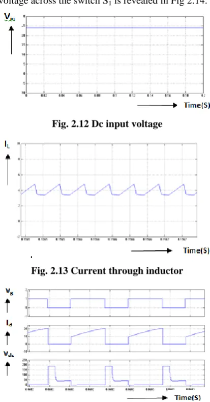
The DC input voltage is revealed in Fig 2.12.The current through the inductor L is revealed in Fig 2.13. The switching pulse given to the gate and the drain current and the voltage across the switch S1 is revealed in Fig 2.14.
Fig. 2.12 Dc input voltage
Fig. 2.13 Current through inductor
Fig. 2.14 Gate pulse, drain Current and voltage across switch S1
[image:3.595.65.273.256.389.2] [image:3.595.63.277.457.613.2]Fig. 2.15 Current through coupled inductor
[image:4.595.67.268.61.180.2]Fig. 2.16 Output voltage
[image:4.595.63.276.179.698.2]Fig. 2.17 Output power
Fig. 2.18 Input voltage vs Output voltage
The graph for the input voltage and the output voltage for the ripple free input current with high step-up boost SEPIC based DC-DC converter is revealed in Fig 2.18.
Fig. 2.19 Input voltage vs Output power
[image:4.595.325.524.296.441.2]The graph for the input voltage and the output power for the ripple free input current with high step-up boost SEPIC based DC-DC converter is revealed in Fig 2.19.
Fig. 2.20 Input voltage vs Efficiency
The graph for the input voltage and the efficiency for the ripple free input current with high step-up boost SEPIC based DC-DC converter is revealed in Fig 2.20.
Case3:
Modified SEPIC converter with magnetic coupling. The high step-up DC-DC converter based on modified SEPIC converter with magnetic coupling is simulated using the blocks of Simulink. The circuit diagram for high step-up DC-DC converter based on modified SEPIC converter with magnetic coupling is shown in Fig 2.21.
[image:4.595.306.546.600.841.2]Fig. 2.22 Dc input
Fig. 2.23 Current through inductor
Fig. 2.24 Gate pulse, drain Current and voltage across switch S1
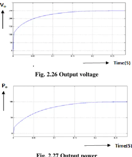
[image:5.595.314.538.357.683.2]The current through the coupled inductor L1 and L2 is revealed in the Fig 2.25. The output voltage and output power for high step-up DC-DC converter based on modified SEPIC converter with magnetic coupling are shown in the Fig 2.26 and Fig 2.27 respectively.
Fig. 2.25 Current through coupled inductor
Fig. 2.27 Output power
Table.1 Comparison of current Ripple, output voltage, output power and Efficiency.
Converte rs
Ior Vin (v)
Vo
(v) Pin (W)
Pou t (W)
%Ef ficie ncy SEPIC
Converte r
0.6 2
24 242 113.
5 94.
5
83.2 %
Ripple free SEPIC converter
0.6 0
24 242 116 94 81%
Modified SEPIC
with Coupled Inductor
0.6 1
24 250 117 100 85.4
%
[image:5.595.63.271.606.729.2]The graph for the input voltage and the output voltage for thehigh step-up DC-DC converter based on modified SEPIC converter with magnetic coupling is revealed in Fig 2.28.
Fig. 2.29 Input voltage vs Output power
[image:6.595.60.279.108.261.2]The graph for the input voltage and the output power for thehigh step-up DC-DC converter based on modified SEPIC converter with magnetic couplingare revealed in Fig 2.29.
Fig. 2.30 Input voltage vs Efficiency
The graph for the input voltage and the efficiency for thehigh step-up DC-DC converter based on modified SEPIC converter with magnetic couplingare revealed in Fig 2.30.
Fig. 2.31 Input voltage vs Output power
[image:6.595.62.277.321.457.2]The graph for the input voltage and the output power with SEPIC and ripple free current for thehigh step-up DC-DC converter are revealed in Fig 2.31.
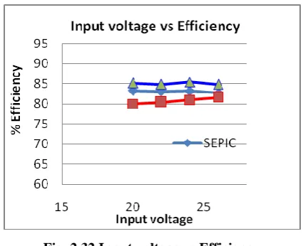
Fig. 2.32 Input voltage vs Efficiency
The graph for the input voltage and the efficiency with SEPIC and ripple free current and the modified SEPIC with magnetic coupling for thehigh step-up DC-DC converter are revealed in Fig 2.32.
III. EXPERIMENTAL-RESULTS:
Hardware-snap shot is exposed to Fig 3.1. The input-voltage is appeared in Fig 3.2. The output input-voltage of battery is free from ripple.
Fig. 3.1 Hardware-Snap-Shot
[image:6.595.313.543.367.842.2] [image:6.595.315.539.369.569.2] [image:6.595.61.279.525.700.2]Fig. 3.3Switching-Pulse & Vds for SEPIC converter
Fig. 3.4Output-Voltage of SEPIC Converter
IV. CONCLUSION
SEPIC with and without coupled inductor based high dc-dc converters are designed; modelled and simulated using MATLAB and the results are presented. The simulation results indicate that the SEPIC with coupled high gain converter system produces output power of 100W with a ripple current of 0.061A.Therefore the coupled inductor based SEPIC converter is better than without coupled inductor based SEPIC converter. The proposed system has advantages like increased output power, reduced ripple and low switching losses. The disadvantages of proposed system are that it requires more hardware components. The scope of the present work is to identify a better modified SEPIC convertersystem to produce high power. The closed loop system using FLC controller will be investigated in future.
REFERENCES
1. -M.Castilla, -L.G.deVicuna, -J.M.Guerrero, -J.Matas, &-J.Miret,‗-Design-of-voltagemode-hysteretic –controllers-for-synchronous-buck-converters –supplying-microprocessor-loads‘, -IEE-Proceedings onElectricalPowerApplications, Vol152, No5, pp1171– 1178, -Sep-2005.
2. M.Castilla,-L.G.deVicuna,-J.M.Guerrero,-J.Miret,& -N.Berbel, ‗-Simple-low-cost-hysteretic-controller for-single-phase-synchronous-buck-converter‘, -IEEE-Trans..,on-P.E,-Vol-22,-No-4,-pp-1232– 1241, -Jul-2007.
3. M.Castilla,-L.G.deVicuna,-J.M.Guerrero,-J.Matas,&-J. Miret, ‗-Designing-VRM-hysteretic-controllers-for optimal-transient-response‘,-IEEE-Tran..,-on-I.E, -Vol.-54, -No-3, -pp-1726–1738, Jun-2007.
4. M.P.KaŸmierkowski,-L.Malesani, ―-Current-Control Techniques-for- Three-Phase-Voltage-Source-PWM-Converters:-A-Survey,‖-in-IEEE-Trans..,-on-I.E, -Vol-45, -No-5, -Oct-1998, pp-691-703.
2012
9. Sabzali, Ahmad J., Esam H. Ismail and Hussain M. Behbehani, "High voltage step up integrated double Boost–Sepic DC–DC converter for fuel cell and photovoltaic applications", Renewable Energy, Vol.82, pp.44-53, 2015
10. Chiu, Huang‐ Jen and Shih‐ Jen Cheng, "Design considerations of an SEPIC PFC converter for driving multiple lighting LED lamps", International Journal of Circuit Theory and Applications, Vol.37, No.8, pp.928-940, 2009
11. Yao, Jia, Alexander Abramovitz and Keyue Ma Smedley, "Analysis and design of charge pump assisted high step up tapped inductor SEPIC converter with an ―inductorless‖ regenerative snubber", IEEE Transactions on Power Electronics, Vol.30, No.10, pp.5565-5580, 2015 12. Di Capua, Giulia, and Nicola Femia, ―A critical investigation of coupled inductors SEPIC design issues", IEEE Transactions on Industrial Electronics, Vol.61, No.6, pp.2724-2734, 2014
13. Tsang, K. M. and W. L. Chan, "Fast acting regenerative DC electronic load based on a SEPIC converter", IEEE transactions on power electronics, Vol.27, No.1, pp.269-275, 2012
14. Park, Ki Bum, Gun Woo Moon and MyungJoongYoun, "Nonisolated high step up boost converter integrated with sepic converter", IEEE transactions on Power Electronics, Vol.25, No.9, pp.2266-2275, 2010 15. Veerachary, Mummadi, "Two loop controlled buck–SEPIC converter
for input source power management", IEEE transactions on industrial electronics, Vol.59, no.11, pp.4075-4087, 2012
[image:7.595.59.279.246.388.2]