Comparing Micro
fl
uidic Performance of Three-Dimensional (3D)
Printing Platforms
Niall P. Macdonald,
†,‡Joan M. Cabot,
†,‡Petr Smejkal,
‡Rosanne M. Guijt,
§Brett Paull,
†,‡and Michael C. Breadmore
*
,†,‡†ARC Centre of Excellence for Electromaterials Science, School of Physical Sciences, University of Tasmania, Sandy Bay, Hobart
7001, Tasmania, Australia
‡Australian Centre for Research on Separation Science, School of Physical Sciences, University of Tasmania, Sandy Bay, Hobart 7001,
Tasmania, Australia
§Pharmacy School of Medicine, University of Tasmania, Hobart 7001, Tasmania, Australia
*
S Supporting InformationABSTRACT: Three-dimensional (3D) printing has emerged as a potential revolutionary technology for the fabrication of microfluidic devices. A direct experimental comparison of the three 3D printing technologies dominating microfluidics was conducted using a Y-junction microfluidic device, the design of which was optimized for each printer: fused deposition molding (FDM), Polyjet, and digital light processing stereo-lithography (DLP-SLA). Printer performance was evaluated in terms of feature size, accuracy, and suitability for mass
manufacturing; laminar flow was studied to assess their
suitability for microfluidics. FDM was suitable for micro-fabrication with minimum features of 321±5μm, and rough surfaces of 10.97 μm. Microfluidic devices >500 μm, rapid
mixing (71%±12% after 5 mm, 100μL/min) was observed, indicating a strength in fabricating micromixers. Polyjet fabricated channels with a minimum size of 205±13μm, and a surface roughness of 0.99μm. Compared with FDM, mixing decreased (27%±10%), but Polyjet printing is more suited for microfluidic applications whereflow splitting is not required, such as cell culture or droplet generators. DLP-SLA fabricated a minimum channel size of 154 ± 10 μm, and 94 ± 7 μm for positive structures such as soft lithography templates, with a roughness of 0.35μm. These results, in addition to low mixing (8%±1%), showed suitability for microfabrication, and microfluidic applications requiring precise control of flow. Through further discussion of the capabilities (and limitations) of these printers, we intend to provide guidance toward the selection of the 3D printing technology most suitable for specific microfluidic applications.
A
dditive manufacturing, or three-dimensional (3D) print-ing, has gained significant attention in manufacturing, because it can directly create 3D designs from a computer-aided drawing (CAD) file. For more than a decade, engineers and designers have been using 3D printers to make prototypes quickly and inexpensively, before embarking on the expensive business of equipping a factory to produce thefinal product. Over time, 3D printing technologies have advanced and been adapted to work with a broad range of materials, including production-grade plastics and metals. Consequently, the technology evolved from a rapid prototyping approach to a manufacturing method, with more than 20% of the output nowin the form of final products.1 3D printing has found
applications in the manufacture of airplanes, shoes, and
clothing, but also in the medical field, providing bone
replacements and dental implants. There has been a significant effort toward exploring the potential of 3D printing for new applications, such as microfluidics and biomedical engineering. While 3D printing wasfirst developed in the 1980s,2there has
been a surge of interest in the implementation of 3D printing in non-traditional areas, with 80% of the academic papers on 3D printing being published in 2012 and beyond.
In thefield of microfluidics, 3D printing offers the capability to directly print complex 3D microfluidic devices with low-cost desktop printers, changing the way in which such devices are conceived, designed, and manufactured. This underpins a potential rapid growth and expansion of industries involved in the manufacturing of portable chemical sensors, as well as diagnostic and biomedical research devices. Providing design and the evaluation of prototype devices within hours at the cost of tens of dollars per device or less, 3D printing provides an attractive alternative to the weeks and hundreds to thousands of dollars typical for traditional microfabrication approaches. In
Received: January 12, 2017
Accepted: March 10, 2017
Published: March 10, 2017
Technical Note
pubs.acs.org/ac
the late 1990s, the introduction of polydimethylsiloxane (PDMS) and soft lithography allowed researchers to prototype with a simple and low-cost infrastructure, significantly expanding microfluidic research. However, PDMS has many known limitations,3 including the complicated commercial translation of academic research, because of difficulties in large volume manufacturing. To this end, 3D printing adds the potential to prototype in materials that are compatible with large volume manufacturingsuch as thermoplastics used in
embossing and injection moldingwith the simplicity,
flexibility, and cost of soft lithography, and may even be a viable manufacturing approach by itself for highly complex 3D geometries, or specialist devices that may only require low to moderate volume production.
The suite of 3D printing technologies has been discussed in detail;4,5 of particular interest for microfluidics are fused deposition molding (FDM), stereolithography (SLA), inkjet/ Polyjet, two photon lithography, selective laser sintering, and layered hydrospinning.6 FDM was first demonstrated as a method for fabricating templates for soft lithography of microfluidic devices with PDMS in 2002,7which was followed shortly thereafter by the same group using an inkjet 3D printer. In 2012, FDM printing was used for the direct fabrication of microfluidic chemical reaction-ware.8 As the resolution and
accessibility of 3D printers has evolved, so too has the complexity of 3D printed microfluidic devices, with recent reports demonstrating direct printing of 3D micromixers9and devices with integrated valves.10 We have shown that 3D printed channels of 250μm×250μm can be achieved by DLP-SLA within a matter of minutes, using commercially available desktop 3D printers,9 and using DLP-SLA with an in-house-developed resin, Nordin et al. fabricated enclosed micro-channels with dimensions of <100μm (60μm×108μm),11as well as integrated valves, pumps, and multiplexors.12 3D printing technology has also found its way into soft robotics with the autonomous microfluidic powered soft octopus,13and our group reported laser sintering for the fabrication of 3D metallic microfluidic devices.14
[image:2.625.63.565.63.392.2]As summarized above, a variety of 3D printing approaches have been used for the fabrication of microfluidic devices, documented in over 100 papers related to 3D printing and microfluidics. This includes several reviews that discuss and contrast the different printing approaches and the devices that have been made by each.6,15−19With a wide range of printers on the market, the suitability for the microfluidic market has been studied by comparing different SLA printers,20different inkjet printers both from Stratasys, and 3D Systems,21as well as a direct comparison between Polyjet and FDM technologies.22
Figure 1.Illustration of 3D fabrication methods, and photographs of 3D printed laminarflow devices with 500μm input channels, and 750μm laminarflow channelfilled with green food dye. (a) FDM method, in which molten plastic is extruded through a heated nozzle, according to the G-code. The features are formed by moving the nozzle in theXY-plane until the current layer was complete, when the build platform was then dropped by a set level (50μm) before moving to the next layer. (b) Polyjet (i3DP) method, where two sets of four-micronozzle arrays (build and support material, respectively) are spraying microdroplets of polymer to form the device. Following each pass, UV lamps polymerize the material before the layer is leveled by a roller and scraper. (c) DLP-SLA method, in which 365 nm light was projected onto a build platform immersed in liquid photopolymer. Following each exposure, the build platform was raised then lowered back into the resin bath for the next 50μm layer. Scale bars = 1 cm.
While these are all valuable contributions, a cross-platform comparison including microfluidic performance is missing.
Here, the three most commonly used printing technologies in microfluidicsFDM, Polyjet, and DLP-SLAare critically compared for their ability to fabricate microfluidic devices. The design of a Y-junction microfluidic device was optimized for each printer, to achieve optimal microfluidic performance. In comparing the devices, consideration was given to the positive and negative feature analysis of SEM images, measurement of surface roughness, production and infrastructure requirements, and a microfluidic performance based on a study of mixing two adjacentflows within the channels. The objective of this report is to provide the information required for informed decision making, as compromises will be required when selecting a 3D printing approach in microfluidics. In a field as diverse as microfluidics, there is not a single 3D printing technology capable of accommodating all the needs, but a technology that best serves each individual application.
■
EXPERIMENTAL SECTIONMaterials. Veroclear-RGD810 print material and SUP707 water-soluble support were purchased from Stratasys, Ltd.
(Eden Prairie, MN, USA). Crystal Clear acrylonitrile−
butadiene−styrene (ABS) 1.75-mm-diameter filament was
purchased from 3D Printing Systems (Melbourne, Australia). BV-007 photopolymer was purchased from MiiCraft (Young Optics, Inc., Hsinchu, Taiwan). Isopropanol, and sodium
hydroxide (NaOH) were purchased from Sigma−Aldrich
(Sydney, Australia). Colored food dyes were purchased locally and used as received. Deionized water was provided, using a Merck Millipore purification system (Bedford, MA, USA).
Instrumentation.The laminarflow devices were designed using SolidWorks 2015−2016 (Dassault Systèmes SE, France), and were printed with a Felix 3.0 (FELIX 3D printers, Nieuwegein, The Netherlands), Objet Eden 260VS professional 3D printer (Stratasys, Ltd., Eden Prairie, MN, USA), and a MiiCraft+ desktop DLP-SLA 3D printer (Young Optics, Inc., Hsinchu, Taiwan). Slicing of .stlfiles into G-code for the Felix 3.0 was completed using KISSlicer v1.5, and printing was controlled by Repetier Host v1.05 (Willich, Germany). Objet Suite v9.211.3626 (Stratasys Ltd., Eden Prairie, MN, USA), sliced and processed models for printing, according to manufacturer guidelines. For the MiiCraft+, devices were sliced using Creation Workshop (DataTree3D, Dallas, TX, USA), and edited in Photoshop Elements 14.1 (Adobe Systems Inc., San Jose, CA, USA) before printing on the MiiCraft+ controller software. Surface data were collected using a Veeco Wyko NT9100 surface profilometer (Bruker Corporation, Billerica, MA, USA), and data were processed with Vision 4.20. SEM images were taken using an Analytical UHR Schottky emission scanning electron microscope (Model SU-70, Hitachi, Chiyoda, Tokyo, Japan). For pumping of dye into the devices, a dual syringe pump (Harvard Apparatus, Inc., Holliston, MA, USA) with 10 mL of disposable plastic was used, with sample volumes of 10 mL for both blue and yellow dyes. Theflow rates selected were 25, 50, and 100μL/min. PEEK tubing OD 1.59, ID 0.508 mm (P/N: 052308) was supplied by Thermo Fisher Scientific (Waltham, MA, USA). For measurement of the fabricated channels and diffusion cones, ImageJ was used.
Fabrication of Laminar Flow Devices. Three methods were used to fabricate the devices: (i) FDM (Felix 3.0), (ii) PolyJet (Eden 260VS), and (iii) DLP-SLA (MiiCraft+). These three methods are depicted inFigure 1. Test parts containing
open and closed channels with 1000, 750, 500, 350, and 250
μm dimensions, with 1:1 ratio and 1:1.5 ratio channels, were printed for analysis and characterization. Because of the limitations in the resolution that can be obtained using the Felix 3.0, only devices containing 1000, 750, and 500 μm channels were produced for comparison with the other printers. All structures were printed and analyzed in triplicate.
FDM Printing. FDM printing involves extruding thermal plastic through a heated nozzle, which was controlled by two precision stepper motors, following coordinates specified by G-code generated using KISSlicer, using the following parameters: layer height, 100μm; extrusion width, 300μm; infill, 100%; 5 mm/s, print speed; 1 loop stroke. After depositing each layer, the build platform was lowered 100μm before extruding the next layer. A single nozzle was used to extrude Crystal Clear ABS at a temperature of 210°C for thefirst layer, 185°C for the rest while the build platform was at 70°C throughout the print. After completion of the print run, reservoirs were cleared of strayfibers. No support material was used.
PolyJet Printing. PolyJet printing involves jetting a photopolymer using linearly arranged nozzles, then spraying microdroplets onto the build surface, where the material was polymerized using an integrated UV light source. Voids in the model werefilled with a support material, which was removed after the printing process had been completed. All devices were fabricated with Veroclear-RGD810 build material, in combina-tion with SUP707 as a water-soluble support. Orientacombina-tion of the devices was always aligned with the print head, so that the roller texture was parallel to the main fluidic microchannel, and printedflat on the build platform in matte mode. To dissolve the soluble support, devices were soaked in water for up to 6 h, depending on the channel size, followed by soaking in 2% NaOH for up to 3 days with sonication, andfinallyflushed with a water jet.
DLP-SLA Printing. DLP-SLA printing involved optically curing a photopolymer through a clear bottomed bath by a digital projector, with the vertical movement of the build platform being controlled by a single stepper motor. Using the projector, each slice of the device was projected onto the bottom of the bath to attach to the build platform. After each exposure, the platform with the previous layer(s) was raised, then lowered to a position minus the height of the previous layer (50 μm in this work). Post-processing of the device involved removal of nonpolymerized resin from the channels using compressed air and bonding the device to a glass microscope slide (25 mm×75 mm) by pressing a glass slide onto the device, onto which a drop of BV-007 resin was placed, before curing by exposure to UV light (365 nm) for 5 min. This bonds the device to a glass base for easier handling, and it post-cures the structure.
■
RESULTS AND DISCUSSIONThree printers were selected for evaluation: FDM, DLP-SLA, and Polyjet. The manufacturer specifications are provided in
Table 1, and schematic representations of the printing processes are shown in the first row of Figure 1, as well as photographs of fabricated devices from each of the printers.
Microfabrication. Initial characterization of the three printers was performed by printing a series of positive and negative structures (data shown inTable 1, andFigure 2shows, in SEM images, a small piece of the template that has both 250 and 350μm open and closed channels. The channels from the FDM printer (Figure 2a) did not form, according to the design.
There were polymer beads making connecting channels (features“1” and “2” in Figure 2a) and rough and deformed areas where the nozzle changed direction (feature“3”inFigure 2a). Channels printed with the Polyjet printer (Figure 2b) met the 250 and 350μm channels specified in the design (features “4” and “5” in Figure 2b). The spray and roll process of the PolyJet made for a distinctive texture on the top surfaces, including the bottom/top surface of the channel (feature“5”in
Figure 2b). The height of each layer was 17.3±2.4μm (n= 12), which is close to the 16 μm specified by the printer manufacturer, causing a layering effect in the sidewalls (feature “4”inFigure 2). The top cover for the closed channels had an organic, grown appearance at the edge (feature“6” inFigure 2b), which was due to the interaction between the support and the build material. Channels fabricated by the DLP-SLA (Figure 2c) were the closest in appearance to a device fabricated with traditional microfabrication methods, with straight sidewalls. The height of each layer was 37 ± 1 μm (n= 3) with a roughness (Ra) of 3 μm (feature “7”inFigure 2c). The grid texture on the top surfaces, including inside the microchannel, appeared because of the pixels (56μm×56μm) from the projector CCD and uneven illumination from each
pixel. Back-exposure was a significant issue, as the closed channels would often block (feature “8” in Figure 2) the pathway when the resin trapped in the channel was exposed; careful optimization of the print parameters was required to avoid this.
The correlation between the size of the designed and fabricated channels is shown in Figure 3. All of the printers demonstrated a linear correlation; however, the accuracy and precision varied.
[image:4.625.327.560.173.358.2]Using FDM, it was impossible to fabricate chips with channels smaller than 500 μm, which correlates with the findings by Lee et al.,22and channels were consistently smaller (−107±36μm) than designed; this is due to spreading of the polymer as it is extruded. It was observed that the diameter of the nozzle had significant impact on the channel width; however, it is possible to fabricate channels <500 μm by reducing the distance between deposition passes, as demon-strated by Anciaux et al.23Fabrication by the PolyJet was found to produce slightly smaller channels (−40 ± 36 μm), with a similar deviation to the FDM. Closed and open channels as
Table 1. Comparison of Fabrication, and Production Factors
of Microfluidic Devices for the 3D Printers in This Work
FDM (Felix 3.0)
Polyjet (Eden 260VS)
DLP-SLA (Miicraft+)
Fabrication Factors
printer resolution XYZ (μm)
300×300 ×50
250×250×16 56×56×50
+ve feature min (μm) 321±5 270±70 94±7
−ve feature min (μm) 370±7 205±13 154±10 build areas XYZ (mm) 240×205
×235
255×252×200 43×27× 180 surface roughness,Ra
(μm) 10.97 0.99 0.35 mixing−5 mm, at 100
μL/min (%)
71±12 27±10 3±1
multi-materials yes (2) yes (2−but one is the support)
no
biocompatible materials ABS,19 PLA29
MED61027 not available
Production Factors
[image:4.625.68.562.599.709.2]post-processing <1 h >1 day <15 min time per chip (mins) 6 30 12 chips per hour 10 33 4 cost per chip (USD) 0.1 4 2 cost per printer (USD) 1.3 k 85 k 3 k
Figure 2.SEM micrographs of open and closed microfluidic channels: (a) FDM structure, where (1) 250μm channels and (2) 350μm channels are visible, as well as (3) deformed surface due to nozzle; (b) PolyJet structure with (4) a layer thickness of 16μm, (5) the surface texture due to the scraper, and (6) deformed layers due to support interaction; and (c) DLP-SLA structure with (7) a layer thickness of 32±2μm, (8) underexposure causing partial collapse of the channel, and (9) texture due to projector pixels (56μm). Scale bars = 500μm.
Figure 3.Graph showing the relationship between CAD design and fabricated channels for the three printing technologies. PolyJet (black diamond (◇), large dashed line) shows a tendency to undershoot (40
±36μm), FDM (red square (□), small dashed line) also undershot by >100μm (109±37μm); however, DLP-SLA (green triangle (△), solid line) demonstrated a tendency to overshoot (26±20μm); DLP-SLA demonstrated the closest to a direct replication of the original CAD design. All measurements were taken from SEM images using ImageJ.N= 3.
small as 205 ± 13 μm (designed 250μm) were printed and successfully cleared of support material.
The PolyJet was the only printer capable of reproducing channels of this size; however, it struggled to fabricate positive
features smaller than 200 μm, which is typical of the
technology.21
The DLP-SLA printer was the only printer to produce channels slightly larger than the design (26±20 μm), which corresponds to half a pixel (56 μm × 56 μm), and was the highest in accuracy and precision. In addition, the DLP-SLA was able to fabricate positive structures as small as 94 ± 7, typical of DLP-SLA printers.9,12 The superior accuracy and precision of the DLP-SLA makes this the better choice for microfabrication; however, it cannot match the performance of traditional photolithography and soft-lithography processes.
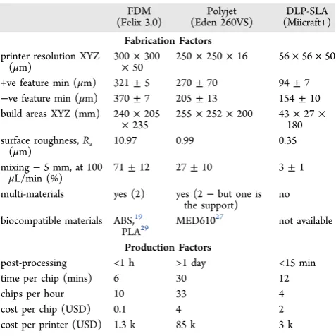
Surface Roughness. To obtain a more quantitative understanding of surface roughness, each device was analyzed with an optical profiler, with the surface profiler renderings shown inFigure 4.
The FDM (Ra= 10.97μm) top surface, shown inFigure 4a, contains a wide range in heights across the surface, varying as much as 93 ± 5 μm. Valley-like formations that had formed through the individual depositions of ABS were observed, with a peak-to-peak distance of 603±55μm, which corresponds to the width of the nozzle diameter. The Polyjet produced a surface with smaller features (Ra= 0.99μm), but the texture of the roller used to level each deposited layer can been observed inFigure 4b. This leads to the formation of troughs 5.8±1μm deep and fish-bone-like textures 1 μm (0.97 ± 1 μm) high, spaced every 147± 15μm. Originating with the roller, these textures are typical of PolyJet or MultiJet printing.21,22 The surface with the smallest features on the surface was obtained
with DLP-SLA (Ra = 0.35 μm, Figure 4c). As already
mentioned, the grid pixel texture (57.5 ± 0.01 μm) was
formed due to CCD pixel density, and resulted in a 0.73±0.14
μm variation in height. The DLP-SLA was found to produce
the smoothest surface of the compared 3D printers, while FDM made the roughest.
Production and Infrastructure.Post-production for each of the three printers was different, with the times for each compared in Table 1. Post-production of FDM devices was simple in that only the removal of strayfibers from connectors was required immediately after printing; however, because the layers left gaps between the port and the tubing, sealant/glue was needed to prevent leaking, which required 1 h to fully cure. For the PolyJet, post-production was a significant issue, because removal of the support material would require up to 3 days to remove from the channels. This is due to the requirement to solubilize the support in water, which was slow for long and narrow channels. This is the main restriction limiting the fabrication of very small (<150μm) channels and new support materials are needed if this is to be achieved.
For DLP-SLA, the post-production was minimal, only requiring bonding the device to a glass slide with resin and exposure to UV light. The simplicity allowed a device to be ready for use within 15 min. DLP-SLA possesses a strong advantage being able to fabricate channels with no support, but optimization of the resin for resolution, optical clarity, and back-exposure reduction needs considerable development. This has already been examined by Gong et al. were closed channels of 60μm×108μm were achieved.11
[image:5.625.64.565.61.277.2]Materials.The device materials in this work were selected for optical transparency over all other factors, as this is desirable for many microfluidic applications. Issues around biocompat-ibility have been investigated in other works; generally, photopolymers are inherently more toxic, because of residual initiator and monomers.22,24−26There are some biocompatible materials marketed for both SLA20 and Polyjet27 printers; however, these still show some toxicity without extensive treatment.24As FDM does not rely on photopolymerization, it has a significant advantage over the DLP-SLA, as well as PolyJet technologies, in terms of biocompatibility. However, ABS is not always inherently biocompatible but can be made so by
Figure 4.Surface roughness renders of (a) FDM, (b) PolyJet, and (c) DLP-SLA. In panel (a), major characteristics of the FDM are shown, with large valleys (peak to peak = 602±55μm) formed due to the individual bead depositions of thermal polymer, and defined by the nozzle diameter (300μm). In panel (b), the texture of the roller used to level each layer is shown, where 5.8±1μm deep troughs are formed, and repeated 1μm highfish-bone-like textures, 0.97±1μm. In panel (c), the pixel texture shown (57.5±0.01μm) has formed due to CCD pixel density, and is repeated throughout the printed surfaces, which were 0.73±0.14μm in height. Measurements taken using Vision 4.20.N= 3.
acetone-based sealing and polyethyl glycol (PEG) grafting.28 PLA would be a more suitable choice for biocompatibility,29 although the transparency of devices is an issue. Commercial translation of research devices into products requires trans-lation of prototypes to injection molding and hot embossing; vacuum casting requires thermoplastics, making FDM attractive. Both FDM and Polyjet printers have the ability to print devices made from multiple materials, and to blend these materials during the printing process. A wide variety of materials is available, with differences in physicochemical properties including, chemical resistance, thermal resistance, flexibility, electrical conductivity, magnetism, and porosity.
Cost.The cost of the printers, both capital, consumable and time costs varies significantly as shown inTable 1. At the time of writing, the approximate cost of the FDM printer used in this work, the Felix 3.0 was $1300 USD, the Eden 260VS was $85 000 USD, and the MiiCraft+ was $3000 USD. A sizable cost difference also exists in the cost of chips, considering the cost of material, not upkeep of the printers, with the price per device being $0.1 USD, $4 USD, and $2 USD for FDM, PolyJet, and DLP-SLA, respectively. It is worth noting that these are still considerably less expensive than the $215 USD estimated for a new PDMS design.15The time to print a device was 6, 30, and 12 min for FDM, PolyJet, and DLP-SLA, respectively. Note that the FDM and DLP-SLA could only print one chip at a time, because of technical limitations. The FDM build platform was not uniformly level; this meant that the calibration of the zero position of the nozzle in theZ-axis had to be established for different XY positions. For the DLP-SLA, the limited XY (43 mm×27 mm) build space meant that the chip design used the entire XY build area; the alternative build orientation of placing the chip length-ways in relation to the Z-axis would have increased build time significantly. The maximal number of chips printed per hour was 10 for the FDM and 4 for the DLP-SLA. In a single, 2 h run, the PolyJet was able to fabricate 66 chips, providing the possibility to produce several hundred devices in a day, making it potentially attractive for small-volume manufacturing. One should keep in mind, however, that the extensive post-processing that is required for PolyJet printing currently limits the attractiveness of this option for same-day prototyping. To summarize, FDM provides chips at a low cost at the expense of resolution, while the Polyjet provides the inverse. DLP-SLA offers high resolution at the expense of throughput, with a cost significantly below than of the Polyjet.
Laminar Flow Chip Design. To examine the fluidic properties of the printed devices, a simple Y junction design was selected for laminarflow studies and fabricated with each of the 3D printers. This design was selected in order to determine the optimized settings for each of the three printers, since it can be used for mixing, reaction, and parallel two-phaseflow. The width and shape of the diffusion area formed between the two flows was examined as a way to determine differences in microfluidic behavior for the three print methods.
While each of the designs had the same internal channel dimensions, careful consideration of the different methods of 3D printing was considered to optimize the device for each printer type. The footprint of the chip was chosen to be 40 mm
×20 mm, as the max XY build space of the MiiCraft+ was 43
mm × 27 mm. The minimum channel size included in the
comparison was 500μm, limited by the smallest dimension that could be printed on the FDM printer.
PolyJet Design.We observed that the VeroClear polymer was brittle and prone to cracking when <1 mm in thickness; hence, devices with a thickness of >1 mm were printed with the PolyJet to retain strength and ease of handling. While brittle at the smaller thickness, once >1 mm in thickness, the chips were difficult to snap or bend. Vertical connectors were designed with straight sidewalls, 100μm less in diameter, which are less than the connecting PEEK tubing (1.6 mm), to provide a tight fit. The rough sidewalls due to the 16 μm layer deposition allowed fluidic sealing at the flow rates examined. Since the negative minimum feature size for the Polyjet was found to be 205± 13 μm, rulers were included in the design to aid with mixing measurements.
FDM Design. With the FDM device, the channel was difficult to visualize once multiple layers of polymer were deposited under the channel to form the chip base. This was due to the cross-hatch nature of the base and entrapment of air between thefilament, due to incomplete fusing of the extruded polymer. The optical clarity was improved by reducing the base layer to a single 100 μm layer, because the ABS was strong enough to be removed from the build platform without deforming or causing leaks. In addition, because of the strength of the ABS, it was possible to reduce the material in the device, which saves material and print time. When forming the 500μm channels, the printer would direct the nozzle across the channel, providing a risk of a small bead of ABS blocking the channel. To overcome this, the walls of the chip were designed to be exactly 3 layers of ABS wide (900μm), and the loop pass number in the software was increased to 3. Therefore, the channels were formed by continuous movements of the nozzle head, with no crossover. The inlets of the devices printed by FDM were designed to address two problems. First, by reducing the height of the device, the print time per device was reduced from 30 min to 10 min. Second, the inlets into which tubing was connected were oriented horizontally, reducing the effective gap around the inserted tubing and improving sealing to the tubing. This also avoided the circular structures required for vertical connection ports, which normally are fabricated in a spiral, leaving a gap equal to the nozzle head diameter.
DLP-SLA Design. Printing using the DLP-SLA was most difficult to optimize of the three printers. Variables in fabrication conditions (room temperature, exposure times, Teflon film position, slicing software, resin age) all impacted the outcome. The final design was reached for four reasons. First, by making the bottom layer of the chip relatively thick (500μm), the structural stability of the device was sufficient to provide the robustness required for easily handling. A minimum of 4 layers (or 200μm) was required to seal the channels and avoid back-exposure into the channel. Second, the fluidic connector went through numerous design iterations, minimiz-ing back-exposure in both vertical and horizontal config-urations. Thefinal design involved tapered connectors from 5 mm to 2.5 mm, and removing the section directly above the channel. Third, as the sidewall roughness was <1μm, sealing of the tubing without sealant was an issue. To address this, a collar with a reduced diameter of 1.4 mm was introduced to grip the tubing and seal the connector. Fourth, the forces between the cured layer and Teflonfilm caused devices to stick to the build space; this effect increases with surface area. Therefore, by reducing the surface area by removing sections of the bulk next to the laminarflow channels, we prevented sticking while still providing structural integrity of the device.
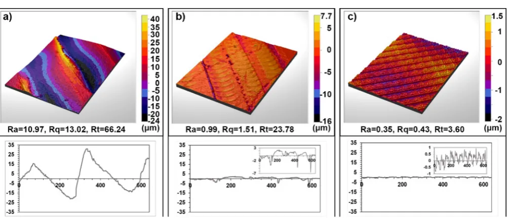
Microfluidics−Laminar Flow and Mixing.The suitability of the chips fabricated by the three 3D printers for microfluidics was studied. Laminarflow profiles at aflow rate of 25μL/min are shown inFigure 5of FDM (Figure 5a), PolyJet (Figure 5b), and DLP-SLA (Figure 5c). The extent of mixing forflow rates of 100, 50, and 25μL/min, respectively, are shown below the flow photographs for each printer.
FDM Microfluidics.In the FDM chips, the two dyes started flowing parallel, but mixed rapidly with complete mixing achieved within 15 mm from the intersection for allflow rates. The large peaks and valleys formed through the fabrication process (Figure 4) cause additional flow interfaces with folds and stretches as described by Simonnet and Groisman.30This mixing occurs when theflow from one of the inlets was parallel to the printed grain in the chip. Considering the popularity of surface patterning for the creation of passive micromixers, FDM
may be a simple and effective way to make micromixers.
Alternatively, their use should be restricted to applications where mixing has no impact on the outcome.
[image:7.625.66.564.65.303.2]PolyJet Microfluidics. In the PolyJet chips, the fluids reached complete mixing at 25 mm for 50μL/min, and 15 mm for 25μL/min. Unexpected mixing was observed at the origin, which we believe was caused by the 16μm channel structures present in the sidewalls running parallel to theflow profile (see
Figure 5). At high flow rates (100 μL/min), this effect was reduced and mixing was 83%±6% at 25 mm. At 25μL/min, however, more mixing was observed at 5 mm than when using
FDM printed devices (82% ±6% vs 71% ±12% for PolyJet
and FDM, respectively). Microfluidic devices, where complex geometries are required without the need for precision in
channel reproduction, such as droplet or cell culture systems, are most suited to PolyJet-type printers.
DLP-SLA Microfluidics. The DLP-SLA chips showed the least mixing, and complete mixing was not achieved at any of theflow rates shown (complete mixing only occurred at 1μL/ min). The highest extent of mixing was 32%±7% at 25 mm and 25 μL/min. These results are in agreement with the low surface roughness (Figure 4) and high design reproducibility (Figure 3), and the results provideflow profiles similar to those observed in more conventionally fabricated devices.31 Micro-fluidic devices that require laminar flow and minimization of mixing (for example, diffusion based H-filters) are most suited to be made with these types of printers.
■
CONCLUSIONSComparing the performance of the three most popular three-dimensional (3D) printing technologies used to make micro-fluidic devices, we found that they all have significant advantages. While microchannel resolution generally is still a major issue for all 3D printers, each of the different types of printers has unique properties when it comes to making microfluidic devices.
FDM printers are the least expensive, with regard to both purchase and operate, and have the largest selection in material
choice−some of which are biocompatible (PLA, COC),
electrically conductive (composites with carbon, cooper, graphene), and have specific chemical resistance (COC, for example, which is resistant to hydrolysis, acids, alkalis, as well as polar solvents such as methanol). Its reliance on thermoplastics inherits compatibility with traditional polymer manufacturing
Figure 5.Microscopic images of laminarflow within 500μm×500μm channels into 750μm×500μm channels, visualized with yellow and blue food dye at 25μL/min for FDM, Polyjet, and DLP-SLA respectively. Plots of distance vs mixing ratio, demonstrating diffusion through the laminar
flow channel at 100, 50, and 25μL/min, respectively, are also shown. (a) The FDM (red diamond (◇), large dashed line) shows increased mixing due to the 300-μm-wide valleys formed by the deposition of polymer beads pressing together; theflow rate has little effect on the mixing rate with consistent mixing saturation at 15 mm. (b) The Polyjet (blue square (□), small dashed line) displayed a diffusion cone more similar to what would be expected in devices of this type fabricated with traditional methods. However, pinching can be observed at the origin, with increased mixing compared to the DLP-SLA, and FDM before stabilizing. This was due to the layered 16μm surfaces of the sideways, causing increased mixing, which was reduced at 100μL/min and did not saturate, as did 50μL/min. However, the profile became similar to the FDM at 25μL/min saturating at 15 mm. (c) The DLP-SLA (green triangle (△), solid line) showed stable low levels of mixing for all of theflow rates, with a limited range of error. As theflow rate decreased, the level of mixing also did, however, in a linear fashion with no saturation.N= 3. Scale bar = 500μm.
potentially, helping the translation to commercial products. Multiple material printing is another strong advantage for FDM, which is also shared by the PolyJet. While low resolution (321±5μm) particularly in the XY plane means that <500μm is an impossibility at this stage, the roughness (10.97μm) does make the FDM well-suited for the fabrication of low-cost micromixers.
The Polyjet printer was able to produce the smallest closed channels (205 ± 13 μm) and was capable of producing the largest number of chips per hour (33 chips), making the Polyjet a potentially attractive option for low-volume manufacturing in
research environments. However, the difficulty and time
needed in removing the support complicates post-processing, which is a significant disadvantage. In addition to the high initial purchase price of the printer and high cost of consumables, it has the highest cost per device of the three printers compared. We see the Polyjet being useful for fabricating complex microfluidic systems for droplet generation and cell culture platforms.
The resolution of the DLP-SLA allows for the smallest open channels (154±10μm), with well-defined channels, and fast post-processing. The major advantage for the DLP-SLA devices was the laminar flow performancethe fluidic behavior is similar to what is achieved in current microfluidic devices however, the small XY build space (43 mm×27 mm) limits the throughput, making it mainly suitable for single-device prototyping. Similar to the PolyJet, DLP-SLA relies on the use of commercial photopolymers, inherently compromising biocompatibility. The primary disadvantage of the DLP-SLA is that, because of the fact that a support is not used, back exposure of channels limits closed channel fabrication to 500
μm with our printer. These results indicate the DLP-SLA is well-suited to microfluidics, where precise control of features andfluidics is critical.
The selection of the“best printer for the job”requires careful consideration of the requirements of the device, and application; compromises will have to be made on some aspects, since there is no technology covering all microfluidic applications. We believe that, to ensure that tomorrow’s printers will better cover demands specific to the microfluidic community, communication of these demands through partner-ships and conversation with 3D printing engineers is required.
■
ASSOCIATED CONTENT*
S Supporting InformationThe Supporting Information is available free of charge on the
ACS Publications website at DOI: 10.1021/acs.anal-chem.7b00136.
The Supporting Information includes the .stlfiles of the
500 μm channel devices (FDM, PolyJet, DLP-SLA)
designed, fabricated, and tested in this work. Supporting Information (SI) (.RAR) includes the FDM laminarflow device (.stl), the PolyJet laminarflow device (.stl), and the DLP-SLA laminarflow device (.stl) (ZIP)
■
AUTHOR INFORMATIONCorresponding Author
*E-mail: [email protected].
ORCID
Brett Paull:0000-0001-6373-6582
Michael C. Breadmore: 0000-0001-5591-4326
Author Contributions
N.P.M. designed, fabricated, performed experiments, collected data, and prepared the manuscript; J.M.C. and P.S. assisted with the experiments, and paper editing; R.M.G., M.C.B., and B.P. conceived and supervised the research and edited the paper. All
authors have given approval to the final version of the
manuscript.
Notes
The authors declare no competingfinancial interest.
■
ACKNOWLEDGMENTSDr. Sandrin Feig is thanked for his assistance in SEM imaging. This study is supported by ARC Centre of Excellence for Electromaterials Science (ACES) (Grant No. CE140100012). The authors thank the Central Science Laboratory (CSL). M.C.B. would like to thank the ARC for a Future Fellowship (No. FT130100101). R.M.G. would like to acknowledge the Alexander von Humboldt Foundation for a fellowship for experienced researchers.
■
REFERENCES(1) Sahore, V.; Kumar, S.; Rogers, C. I.; Jensen, J. K.; Sonker, M.; Woolley, A. T.Anal. Bioanal. Chem.2016,408, 599−607.
(2) Hull, C. W. U.S. Patent No. 4,575,330, March 11, 1986. (3) Mukhopadhyay, R.Anal. Chem.2007,79, 3248−3253. (4) Pham, D. T.; Gault, R. S.Int. J. Mach. Tool. Manuf. 1998,38, 1257−1287.
(5) Vaezi, M.; Seitz, H.; Yang, S.Int. J. Adv. Manuf. Technol.2013,67, 1721−1754.
(6) Waheed, S.; Cabot, J. M.; Macdonald, N. P.; Lewis, T.; Guijt, R. M.; Paull, B.; Breadmore, M. C.Lab Chip2016,16, 1993−2013.
(7) McDonald, J. C.; Chabinyc, M. L.; Metallo, S. J.; Anderson, J. R.; Stroock, A. D.; Whitesides, G. M.Anal. Chem.2002,74, 1537−1545. (8) Symes, M. D.; Kitson, P. J.; Yan, J.; Richmond, C. J.; Cooper, G. J. T.; Bowman, R. W.; Vilbrandt, T.; Cronin, L.Nat. Chem.2012,4, 349−354.
(9) Shallan, A. I.; Smejkal, P.; Corban, M.; Guijt, R. M.; Breadmore, M. C.Anal. Chem.2014,86, 3124−3130.
(10) Rogers, C. I.; Qaderi, K.; Woolley, A. T.; Nordin, G. P. Biomicrofluidics2015,9, 9.
(11) Gong, H.; Beauchamp, M.; Perry, S.; Woolley, A. T.; Nordin, G. P.RSC Adv.2015,5, 106621−106632.
(12) Gong, H.; Woolley, A. T.; Nordin, G. P.Lab Chip2016,16, 2450−2458.
(13) Wehner, M.; Truby, R. L.; Fitzgerald, D. J.; Mosadegh, B.; Whitesides, G. M.; Lewis, J. A.; Wood, R. J.Nature2016,536, 451− 455.
(14) Sandron, S.; Heery, B.; Gupta, V.; Collins, D. A.; Nesterenko, E. P.; Nesterenko, P. N.; Talebi, M.; Beirne, S.; Thompson, F.; Wallace, G. G.; Brabazon, D.; Regan, F.; Paull, B.Analyst 2014,139, 6343− 6347.
(15) Au, A. K.; Huynh, W.; Horowitz, L. F.; Folch, A.Angew. Chem., Int. Ed.2016,55, 3862−3881.
(16) Bhattacharjee, N.; Urrios, A.; Kang, S.; Folch, A.Lab Chip2016, 16, 1720−1742.
(17) Chen, C.; Mehl, B. T.; Munshi, A. S.; Townsend, A. D.; Spence, D. M.; Martin, R. S.Anal. Methods2016,8, 6005−6012.
(18) Ho, C. M. B.; Ng, S. H.; Li, K. H. H.; Yoon, Y. J.Lab Chip2015, 15, 3627−3637.
(19) Amin, R.; Knowlton, S.; Hart, A.; Yenilmez, B.; Ghaderinezhad, F.; Katebifar, S.; Messina, M.; Khademhosseini, A.; Tasoglu, S. Biofabrication2016,8, 022001.
(20) Au, A. K.; Lee, W.; Folch, A.Lab Chip2014,14, 1294−1301. (21) Walczak, R.; Adamski, K. J. Micromech. Microeng. 2015, 25, 085013.
(22) Lee, J. M.; Zhang, M.; Yeong, W. Y.Microfluid. Nanofluid.2016, 20, 5.
(23) Anciaux, S. K.; Geiger, M.; Bowser, M. T.Anal. Chem.2016,88, 7675−7682.
(24) Macdonald, N. P.; Zhu, F.; Hall, C. J.; Reboud, J.; Crosier, P. S.; Patton, E. E.; Wlodkowic, D.; Cooper, J. M.Lab Chip2016,16, 291− 297.
(25) Oskui, S. M.; Diamante, G.; Liao, C.; Shi, W.; Gan, J.; Schlenk, D.; Grover, W. H.Environ. Sci. Technol. Lett.2016,3, 1−6.
(26) Urrios, A.; Parra-Cabrera, C.; Bhattacharjee, N.; Gonzalez-Suarez, A. M.; Rigat-Brugarolas, L. G.; Nallapatti, U.; Samitier, J.; DeForest, C. A.; Posas, F.; Garcia-Cordero, J. L.; Folch, A.Lab Chip 2016,16, 2287−2294.
(27) Sayyar, S.; Murray, E.; Thompson, B. C.; Chung, J.; Officer, D. L.; Gambhir, S.; Spinks, G. M.; Wallace, G. G.J. Mater. Chem. B2015, 3, 481−490.
(28) McCullough, E. J.; Yadavalli, V. K. J. Mater. Process. Technol. 2013,213, 947−954.
(29) Athanasiou, K. A.; Niederauer, G. G.; Agrawal, C. M. Biomaterials1996,17, 93−102.
(30) Simonnet, C.; Groisman, A.Phys. Rev. Lett.2005,94, 134501. (31) Hessel, V.; Löwe, H.; Schönfeld, F.Chem. Eng. Sci.2005,60, 2479−2501.