White Rose Research Online URL for this paper:
http://eprints.whiterose.ac.uk/135163/
Version: Published Version
Article:
Dey, A.B., Sanyal, M.K., Farrer, I. orcid.org/0000-0002-3033-4306 et al. (5 more authors)
(2018) Correlating Photoluminescence and Structural Properties of Uncapped and
GaAs-Capped Epitaxial InGaAs Quantum Dots. Scientific Reports , 8. 7514. ISSN
2045-2322
https://doi.org/10.1038/s41598-018-25841-7
[email protected]
https://eprints.whiterose.ac.uk/
Reuse
This article is distributed under the terms of the Creative Commons Attribution (CC BY) licence. This licence
allows you to distribute, remix, tweak, and build upon the work, even commercially, as long as you credit the
authors for the original work. More information and the full terms of the licence here:
https://creativecommons.org/licenses/
Takedown
If you consider content in White Rose Research Online to be in breach of UK law, please notify us by
www nature com scientificreports
Correlating Photoluminescence and
Structural Properties of Uncapped
and GaAs-Capped Epitaxial InGaAs
Quantum Dots
Arka B. Dey , Milan K. Sanyal , Ian Farrer , Karthick Perumal , David A. Ritchie ,
Qianqian Li , Jinsong Wu & Vinayak Dravid
The understanding of the correlation between structural and photoluminescence (PL) properties of self assembled semiconductor quantum dots QDs particularly InGaAs QDs grown on GaAs substrates, is crucial for both fundamental research and optoelectronic device applications. So far structural and PL properties have been probed from two di erent epitaxial layers namely top capped and buried layers respectively Here we report for the rst time both structural and PL measurements from an uncapped layer of InGaAs QDs to correlate directly composition, strain and shape of QDs with the optical properties. Synchrotron X-ray scattering measurements show migration of In atom from the apex of QDs giving systematic reduction of height and enlargement of QDs base in the capping process The optical transitions show systematic reduction in the energy of ground state and the rst excited state transition lines with increase in capping but the energy of the second excited state line remain unchanged We also found that the excitons are con ned at the base region of these elliptically shaped QDs showing an interesting volume dependent con nement energy scaling of instead of
expected for spherical dots The presented method will help us tuning the growth of QDs to achieve desired optical properties.
Semiconductor quantum dots (QDs), where charge carriers are conined in all three directions on length scales of a few nanometers, resulting in discrete energy levels, are fascinating size-tunable photonic materials providing narrow line-width emissions1. In the last few years, signiicant attempts have been made to apply these QDs in
realizing large-scale quantum processors2, large-area display3, solar cells beyond Shockley-Queisser limit4, and
electronic-photonic devices5,6. Although QDs can be grown by various physical and chemical techniques ranging
from Molecular Beam Epitaxy (MBE) to solution processing7, epitaxial QDs of semiconductors, grown in MBE
on a single-crystal substrate having a speciic crystallographic orientation, provide us with well-deined systems to correlate optical and structural properties. Indium-Gallium-Arsenide (InGaAs) QDs on Gallium-Arsenide (GaAs) (001) substrate, is the best candidate for mid and far infrared photodetectors and as the active material in photovoltaic ields and are the most studied system to understand structure-tunable optical emissions. A sub-stantial amount of research work has been done to correlate emission-wavelength, line-shape and the efect of spin-orbit coupling in quantum yield of the QDs with the composition and strain proiles. he shapes of QDs, apart from size and structure tuning, have also been used as a controlling parameter to tune optical properties. he QDs of various shapes have been grown, like ellipsoidal8, lens9,10, pyramidal11, multi-faceted11 and quantum
rings12. In all these studies6,13–17 optical signals were obtained from a buried layer, that reduces non-photonic
transitions of exposed surface, and measurements of structural parameters namely composition, strain, size and shape were obtained from the capped top layer, with a key assumption that the buried and surface QD layers are identical in nature.
Surface Physics Material Science Division Saha Institute of Nuclear Physics AF Bidhannagar Kolkata India Department of Electronic and Electrical Engineering University of She eld Mappin Street She eld S
JD United Kingdom Deutsches Elecktronen Synchrotron DESY Notkestrasse Hamburg Germany Cavendish Laboratory University of Cambridge J J Thomson Avenue Cambridge CB HE United Kingdom Department of Materials Science and Engineering Northwestern University Evanston IL USA Correspondence and requests for materials should be addressed to M K S email milank sanyal saha ac in) Received: 7 December 2017
Accepted: 30 April 2018
Published: xx xx xxxx
However, it is becoming increasingly clear that this assumption is not in fact valid as In-Ga intermixing during growth of these two layers on GaAs (001) substrate, the buried-layer just above the bufer layer and the top-layer just below capping layer can be quite diferent. he process of strain release18, segregation, faceting, intermixing,
and strain-enhanced difusion between layers of QDs near bufer and capped layers known to vary19,20 strongly
afecting the coninement length of charge carriers within QDs that determine the characteristics of emitted photons15–17. Here we show, for the irst time, that both structural and optical properties can be measured from
same layer of QDs as a function of capping layer thickness. he atomic force microscopy (AFM) images obtained from uncapped QD sample enabled us to reconirm the results obtained from synchrotron X-ray scattering measurements.
Grazing incidence difraction (GID) X-ray measurements14,21–28 are ideal non-destructive techniques to
extract the structural information of the nanometer-thin layer of QDs averaged over a large area depending on the footprint of the X-ray beam over a sample. GID studies reveal the average values of the structural param-eters; composition, interfacial strain, lateral and vertical coninement lengths which are solely responsible for excitonic energy levels within QDs. he availability of intense synchrotron sources delivering nanometer-sized beams would enable us, in the future, to obtain information regarding composition and strain proiles averaged of a few tens of dots or perhaps an individual QD using the methods described in this paper. Here we present the results of uncapped and capped InGaAs QDs samples and the details of data analysis and measurements are given in the method section. It should be mentioned here that the volume of QDs on GaAs substrate is quite small, as a result only GID peaks like the (200), (220), (400) etc can be measured29 nondestructively. Measurement of other
conventional difraction peaks require much higher incidence angle and GaAs peaks overshadows the QD data as the X-ray beam penetrates deeper into the substrate. We optimized the sensitivity of QD signal by varying the incident angle and available energy of the X-ray beam for these measurements. he ratio of integrated intensity of the (200) and (400) proiles from GaAs to InAs in-plane relection are measured here as a function of in-plane lattice parameters to extract indium proile within an average quantum dot.
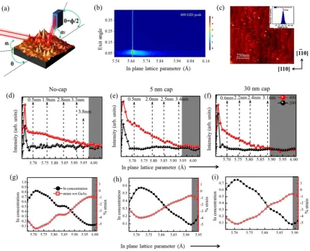
he measurements of (400) and (200) in-plane crystal planes of the QDs samples around the GaAs bulk peaks were done by orienting the substrate at an angle ‘θ’ with incident X-ray beam and 1D Mythen detector is kept at a detector angle (Φ) with respect to direct beam so that it is twice the incident angle of photons to crystal planes (Φ= 2θ) and the scattering geometry is shown in Fig. 1a. hese scans provide direct measure of in-plane lattice parameter (aII) defined in terms of the indices (h, k, l) of the nearest Bragg reflection of the substrate as
λ Φ
= + +
aII h2 k2 l2/(2sin( /2)). Measured scattering intensity taken by 1D Mythen detector data for diferent ‘θ’ values from the obtained scans have been stitched by Matlab programs to generate typical two-dimensional GID images around 400 and 200 Bragg peaks where vertical and horizontal axes denotes exit angle of Mythen detector (αf) and in-plane lattice parameter (aII) respectively. A representative 2D scattered intensity data around
(400) Bragg peak of the uncapped InGaAs QDs is shown in Fig. 1b. We could not detect the signature of a pure InAs difraction peak as the deposition amount of InAs was kept very small (1.8 MLs) and it is known to intermix with GaAs to form InGaAs QDs. Scattered intensity in-between the two extreme aII values (0.565 nm for GaAs and
0.605 nm for InAs) exhibit intermixing and alloying of In and Ga within wetting layer (WL) and QDs. he results from AFM measurements presented here clearly show that the InGaAs QDs are ellipsoidal in shape with a pre-ferred elongation in the direction perpendicular to the miscut stair-steps (refer Fig. 1c). We performed both radial and angular momentum scans in GID around in-plane 400 and 200 Bragg difraction peaks of GaAs, by keeping incidence angle of the X-ray beam below or around the critical angle of GaAs to make the technique sensitive to QDs layer near the surface (refer method section for details). Representative plots of the I400 and I200 proiles have
been shown for uncapped QDs (Fig. 1d) and capped QDs with 5 nm (Fig. 1e) and 30 nm (Fig. 1f) GaAs. It is to be noted here that in 400 and 200 Bragg peaks contribution of GaAs arises from both the substrate and the cap layer. Scattered intensity reduces towards higher in-plane lattice parameter and reaches background counts when
aII= 0.597 nm for uncapped, aII= 0.593 nm for 5 nm capped and aII= 0.589 nm for 30 nm capped QDs. his
sys-tematic reduction in data range may be due to X-ray absorption in increasing GaAs cap thickness. he variation of Indium content as a function of in-plane lattice parameter aII has been calculated using equation (1) given in
method section and the obtained proile reveals compositional variation for diferently capped QDs. It has been found that the concentration x within an average In Gax 1−xAs QD varies between 0.85 and 0.1 as shown in the plot
shown in Fig. 1g for the uncapped sample. For both 5 nm and 30 nm GaAs capped QDs, Indium fraction values reach a maximum of 0.6 and 0.75 respectively as shown in Fig. 1h and i. We shall discuss below the correlation between in-plane lattice parameter aII and the height of an average QD above the substrate by systematic
measure-ments of Yoneda wings and show that aII increases toward the tip of the QD as indicated by vertical lines in
Fig. 1d,e and f. It is clear from these igures that for all three types of samples, Indium content is higher in the lower and middle region of QDs19,30. he in-plane strain proile within QDs with respect to the GaAs were computed
using expressions εII =(aGaAs−a x( ))/ ( )a x, as a function of aII where aGaAs and a(x) are the lattice parameter of
GaAs and of InGaAs obtained from Vegard’s law corresponding to Indium content x31. he calculated strain
www.nature.com/scientificreports/
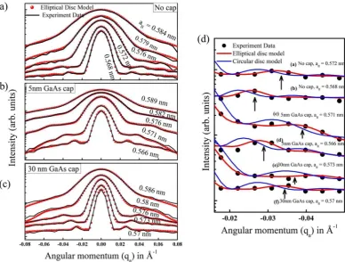
he eccentricity values also increase with increasing capping thickness making buried QDs more elongated (refer Table 1). In Fig. 2d, we have compared the itting quality of circular and elliptical disc model and it is clear from the igure that elliptical disc model represent the experimental data much better (see equation (3), method section). he circular disc model could not represent the data with any diameter as shown in Fig. 2d.
he results presented in Fig. 3a,b and c for uncapped, 5 nm and 30 nm capped QDs clearly show that QD-base region has in-plane lattice parameter aII close to GaAs and with increase in average QD height, aII approach the
value of InAs lattice parameter. For uncapped QDs, refer representative data in Fig. 3a, at the heights 0.5 nm, 1.4 nm, 2 nm, 2.2 nm, 3.3 nm, and 3.8 nm above GaAs substrate the aII values become 0.57 nm, 0.573 nm,
0.576 nm, 0.58 nm, 0.589 nm and 0.593 nm, respectively following equation (5) (refer method section). he data shown in Fig. 3b for 5 nm capped QDs shows a similar trend but the apex region terminates at the aII value of
0.591 nm at a height of 3.4 nm over GaAs substrate indicating migration of the In-atoms from the apex region of QDs with the growth of GaAs cap-layer. In Fig. 3c the data and itted proiles for 30 nm cap-layer are shown and the results indicate further reduction in the heights of QDs to 3.1 nm with the maximum measurable in-plane lattice parameter aII of 0.588 nm.
[image:4.595.105.555.45.409.2]We have carried out systematic AFM measurement of the uncapped QDs to reconirm the elliptical shape obtained from the X-ray analysis. A three-dimensional extracted image of an uncapped QD measured in AFM is shown in Fig. 3d – the elliptical base of 44 ± 4 nm and 25 ± 2 nm in the two mutually perpendicular directions can be clearly seen. It is to be noted here that unlike X-ray measurements the AFM can probe only the portions of uncapped QDs outside wetting layer. he average height of QDs was found to be around 2.2 ± 0.4 nm and we shall
Figure 1. (a) Grazing incidence difraction geometry used in the experiment. Here αi is kept near the critical
discuss detailed comparison of the extracted dimensions below to show that the results of AFM measurements are consistent with the results of the analysis of X-ray data. he AFM data from the other two samples could not be collected due to the presence of capping layers having thickness larger than QD heights. In Fig. 3e we have shown cross-sectional views of uncapped QDs obtained from AFM data along the major and minor axes direc-tions at several measured heights of 0.5 nm, 1 nm, 1.5 nm, 1.85 nm and 2.25 nm. At the 0.5 nm height we obtain major and minor axes as 40.1 ± 4 nm and 23.1 ± 2 nm giving the eccentricity of 0.82 ± 0.05. At the tip region with 2.25 nm height these values become 18.1 ± 2 nm and 11.4 ± 1 nm giving lower eccentricity of 0.77 ± 0.04. At the three intermediate heights of 1 nm, 1.5 nm and 1.85 nm, the representative QD have eccentricity of 0.81 ± 0.05, 0.81 ± 0.04 and 0.78 ± 0.04 with decreasing major axes dimensions of 36.3 ± 3 nm, 32.2 ± 3 nm and 24.6 ± 2 nm respectively. Reductions of eccentricity are also clearly observed from base to tip of uncapped QDs in AFM meas-urements and the obtained values are in reasonable agreement with GID values.
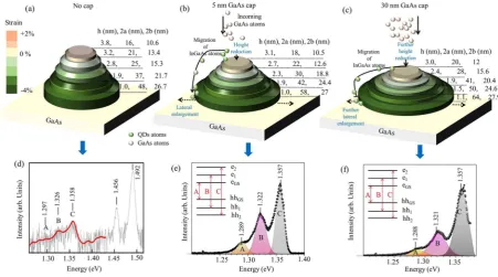
he dimensions of the major and minor axes at the height of 1 nm in GID data comes out to be 48 nm and 26.7 nm giving eccentricity of 0.83 and only at the height of 1.9 nm we get the values of major and minor axes as 37 nm and 21.7 nm with eccentricity of 0.81, refer results of the uncapped sample shown in Fig. 4a. As mentioned earlier the measured height (Fig. 3e) in AFM was found to be about 1.5 nm less than that obtained from X-ray measurements (Fig. 4a) as AFM cannot access portion of QDs buried under wetting layer. he maximum height the particular QD shown in Fig. 3d and average height (3.8 nm) of uncapped QDs obtained from X-ray data also show this diference. he height of QD obtained from X-ray scattering and AFM measurements can be used to
Figure 2. Angular scans (black lines) and itted proiles (red lines) obtained from elliptical iso-strain disc model for (a) uncapped (b) 5 nm and (c) 30 nm capped QDs. (d) Measured angular scan data (black dot) and itted proiles simulated from elliptical (red line) and circular (blue line) iso-strain disc model for (a,b) uncapped InGaAs QDs and (c,d) 5 nm and (e,f) 30 nm capped QDs.
Surface QDs 5 nm GaAs capped QDs 30 nm GaAs capped QDs
aII in nm a (nm) e aII in nm a (nm) e aII in nm a (nm) e
[image:5.595.161.550.45.339.2]0.584 8(1), 2.5(0.28) 0.75 0.589 9(1), 2.5(0.31) 0.8 0.586 10(1), 2.7(0.27) 0.8 0.579 10.5(1), 2.7(0.18) 0.77 0.582 11(1), 2.7(0.14) 0.82 0.58 14(1), 2.6(0.17) 0.83 0.576 12.5(1), 2.7(0.09) 0.79 0.576 15(1), 3(0.1) 0.83 0.576 20(1), 3(0.1) 0.86 0.572 18.5(1), 3.3(0.08) 0.81 0.571 21(1), 2.5(0.07) 0.85 0.573 25(1), 3.3(0.8) 0.87 0.568 24, 3(1), 7(0.07) 0.83 0.566 29(1), 2.5(0.05) 0.87 0.57 32(1), 3.5(0.07) 0.89
www.nature.com/scientificreports/
estimate the wetting layer thickness. he QD density is found to be 60 per µm2 from AFM data of uncapped
quan-tum dot layer giving average surface area per quanquan-tum dot 16667.7 nm2. On the other hand calculated base area
of an average uncapped quantum dot from X-ray scattering measurements come out to be 1006.6 nm2 occupying
only 6% of the surface area of entire wetting layer. he composition of In Gax 1−xAs in the base of an average QD
(refer discussion on PL below) or that of the wetting layer is around x = 0.25 and 1.8 monolayer of deposited InAs would have given us 2.0 nm of wetting layer if there was no QD formation. An average QD has volume of 3825 (=1006.6 * 3.8) nm3 for uncapped QDs layer with an average x = 0.4 and that is equivalent to the volume of 6120
(=3825 * 0.4/0.25) nm3 for x = 0.25. his reduces the thickness of the wetting layer of area 16667.7 nm2 allocated
to each QD to about 1.6 nm - close to the observed difference of QD heights between X-ray and AFM measurements.
We have carried out systematic cross-sectional transmission electron microscopy (X-TEM) measurements32,33
to cross-check the dimensions of the QDs and the estimated thickness of the wetting layer. A representative image of an uncapped QD having height of about ~3.8 nm is shown in Fig. 3f. he obtained height values are found to be consistent with the X-ray and AFM results presented here. Base dimension of 20 nm can be related to the minor axes dimension of elliptical-shaped QD. To determine wetting layer thickness we took X-TEM data in between QDs and the thickness of the measured rough surface giving higher contrast was determined to be around 1.5 nm as indicated by yellow dotted lines in Fig. 3g. his value matches well with the estimated wetting layer thickness.
[image:6.595.99.551.45.386.2]With increasing height of QD, lateral dimensions reduce signiicantly and major and minor axes dimensions become 16 nm and 10.6 nm with eccentricity of 0.75 at the apex region of QD – this is also consistent with meas-ured AFM value. he strain proile obtained from X-ray measurements has been indicated by the color-bar in the Fig. 4. Similar trends have been observed in the GID data on GaAs capped QDs; obtained results are schemati-cally demonstrated in Fig. 4b and c for 5 nm and 30 nm GaAs capped QDs respectively. Tip region of 5 nm capped
Figure 3. Line proiles of scattered intensity with respect to the ratio of exit angle of Mythen detector and critical angle of substrate for diferent in-plan lattice parameters of (a) uncapped [aII= 0.57, 0.573, 0.576,
0.58, 0.589, 0.593, 0.596 in nm] (b) 5 nm [aII= 0.57, 0.574, 0.578, 0.584, 0.587, 0.591 in nm] and (c) 30 nm
[aII= 0.57, 0.572, 0.576, 0.58, 0.588 in nm] capped QDs [for aII values top to bottom in the curves]. (d) Lateral
QDs obtained from X-ray analysis (refer Fig. 4b) show the average maximum height of QDs to be 3.1 nm with major and minor axes dimensions of 18 nm and 10.5 nm respectively. he shape of the uncapped, 5 nm and 30 nm capped QDs shown in Fig. 3e show much larger lateral dimension as compared to height and these QDs can be approximated as elliptical lenses. We notice increase in lateral size and reduction in height of the QD lenses as the capping thickness increases. For 30 nm capping (refer Fig. 3c) major axis dimension (and eccentricity) becomes 64 nm (0.89) and 20 nm (0.8) at height of 1.1 nm and at the tip region with height 3 nm respectively. he shape changes upon capping have been studied34,35 earlier but direct correlations between PL energy and structural
parameters were not investigated.
he micro-PL measurements on uncapped and capped In Gax 1−xAs QDs show presence of three transition
lines36 involving ground state (E ),
GS first excited state (E1) and second excited state (E2) around 1297 meV,
1326 meV and 1356 meV respectively, as indicated by ‘A’, ‘B’ and ‘C’ in Fig. 4d,e and f. It is known that in-plane compressive strain induced out-of-plane tensile strain breaks heavy-hole (HH) and light-hole (LH) at the Γ point (k= 0) degeneracy leading HH-band as efective valence band for optical transition. herefore ‘A’, ‘B’ and ‘C’ has been correlated with transition lines between eGS−hhGS, e1−hh1 and e2−hh2. Although generally EGS peak is
expected to be more intense than E1 and E2, here we observe stronger E1 and E2 lines for all the QD samples. he
high incident excitation intensity used here to get micro-PL data may lead to such intensity reversal due to state filling effects37. As expected the PL emission from the uncapped QD sample was much weaker due to
non-radiative emission process13 through surface states, compared to capped samples. We have used 10 points
(red line) data smoothening for guide to eye and presented in Fig. 4d both measured and smoothed data -the PL peak positions for uncapped QDs are not afected by smoothing process. he presence of strong heavy-hole free exciton (HHFE) PL emission from InGaAs wetting layer around 1450 meV38,39 and similar emission from GaAs
around 1490 meV for all the QDs samples were conirmed. he width38 of the emissions for all the samples were
found to be around 20 meV (refer Table 2) and this value is around half of the width observed in solution pro-cessed QDs used for technological applications2–7. We observed, except for E
2 emission line, that uncapped
sam-ple produces sharper (refer FWHM values Table 2) PL lines.
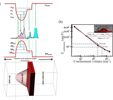
he relationship between QDs structure and conined exciton energy levels are schematically shown in Fig. 5a; the obtained optical transition lines are directly associated with the allowed exciton transitions. he value of EGS
arise from the contribution of (i) composition dependent bulk band gap energy, (ii) coninement size and shape dependent coninement energy and (iii) exciton binding energy. he lateral dimension of the QD elliptical lens becomes larger as the capping thickness increase. he excitonic coninement volume of the average QD elliptical lens can be written as, = π +
Vlens (4h 3 )L
h
24
2 2, where L is the lateral coninement dimension and h is the height. It
[image:7.595.99.551.45.296.2]www.nature.com/scientificreports/
is 0.67 due to the fact that Econfinement~1/r2 for sphere of radius ‘r’. As the shape of coninement deviate from perfect sphere the power factor (γ) reduce from 0.67 to 0.43 (for cuboid shape) and to 0.33 (for pyramidal shape)34. E
confinement for lens shaped QD are calculated by using electron ground state energy and heavy-hole
ground state energy40; we found γ to be 0.3 from the plot of the coninement energy variation with respect to
coninement volume (refer Fig. 5b). Coninement energy for lens shaped QDs found to be primarily controlled by the highest lateral coninement dimension, which is the major length of base region of QDs. We obtained the coninement volume of 2049 nm3 and 4080 nm3 for 30 nm capped and uncapped QDs respectively from GID
measurements, which indicate the coninement energy as 121.6 meV and 96.4 meV (refer blue and green lines in Fig. 5b) for 30 nm capped and uncapped QDs respectively. he measured ground state PL emission energy (EGS)
can be used to calculate efective composition of In Gax 1−xAs as experienced by exciton within the conined
vol-ume V of QDs. For 30 nm capped QDs we get EGS=1288 meV, therefore ater subtracting exciton binding energy (~10 meV) and coninement energy, we found composition dependent band gap energy of 1256.4 meV; indicating
GaAs cap
EGS
(meV)
E1 (meV)
E2 (meV)
E1 – EGS
(meV)
E2 – E1 (meV)
FWHM of
EGS (meV)
FWHM of
E1 (meV)
FWHM of
E2 (meV)
Int. Area of
EGS
Int. Area of
E1
Int. Area of
[image:8.595.167.551.162.501.2]E2 No cap 1297 1326 1358 29 32 12 14 26 0.28 (6.3%) 1.8 (40.5%) 2.36 (53%) 5 nm cap 1290 1323 1357 33 35 24 26 17 1.46 (10.6%) 5.72 (41.6%) 6.58 (47.8%) 15 nm cap 1289 1322 1357 33 35 19 23 17 0.47 (5.9%) 2.9 (36.3%) 4.6 (57.8%) 30 nm cap 1288 1321 1357 33 36 14 21 16 0.37 (5%) 2.66 (36.4%) 4.37 (58.6%)
Table 2. Measured PL emission spectrum and results obtained by itting.
Figure 5. (a) Correlation between structure of QDs and obtained PL lines are linked by the excitonic level formation inside the QDs and WLs. Diferent PL lines (for 5 nm GaAs cap sample) has been associated with the composition and shape dependent exciton levels of QDs. (b) he variation of coninement energy with respect to the conined volume for lens shape InGaAs quantum dots. Black dots are the obtained values of electron ground state energy and heavy hole ground state energy34. Red line is the least square itting of the data points
Indium composition to be x= 0.26. Similarly for uncapped QDs, ground state PL energy of 1297 meV gives the value of Indium composition x= 0.22. It should be noted here that GID measurements also show larger Indium composition in uncapped QDs as compared to 30 nm capped QDs. he Indium composition obtained from PL measurement was found to be lower than the values obtained in GID measurements. his results indicate that excitons are near the base of the elliptical shaped QDs having lower Indium concentration; the coninement area of the excitons, as discussed below, also matched with the dimension of the base of QDs.
We have carried out systematic Gaussian ittings of all the PL emission lines for all four samples having 0 nm, 5 nm, 15 nm and 30 nm GaAs capping and the resultant parameters are shown in Table 2. For uncapped sample the energy spacing, which are essentially decided by the exciton coninement volume, between E2, E1 and EGS are
found to be 32 meV and 29 meV. he energy spacing increases with capping thickness and become 36 meV and 33 meV for 30 nm capped QDs (refer Table 2). he measured separation energy between irst excited and ground state energy (E1−EGS= 3π2ħ2/2 mL2) also reconirmed the consistency of GID and PL measurements. For 33 meV
separation observed in 30 nm capped QDs calculated value of L came out to be 60.3 nm - this is consistent with the obtained major axis of the elliptical base of QDs obtained in the GID measurements. he increase in capping thickness shit PL lines towards lower energy as compare to the uncapped sample; for example a shit of 7 meV and 3 meV for EGS and E1 was observed for 5 nm capping (Table 2) and for 30 nm capping these shits were found
to be 9 meV and 5 meV respectively (Table 2). However no signiicant shit could be detected for the E2 line with
capping.
In conclusion, we have reported a direct method to correlate structural and optical properties of epitaxially grown quantum dots with and without capping. he composition proile of an average QD extracted from GID and PL measurements show that excitons are conined near the base of the QDs. We also found that GaAs capping reduces peak concentration of Indium in the QDs. It will be interesting to extend the presented techniques for the solution processes QDs, which are easy to produce and attractive for display application but we need to ind a way to orient these QDs in preferred crystallographic directions for such GID measurements. We also plan to use this method to probe smaller numbers of dots in future to reduce the efect of statistical averaging and thereby improve our understanding of structure-property correlation in these emerging materials.
Methods
Sample preparation.
A set of samples is grown with similar growth conditions but diferent GaAs capped layer thickness (0–30) nm over InAs QDs on GaAs (001) substrate. he samples were grown by Molecular Beam Epitaxy (MBE). Ater oxide desorption a 250 nm GaAs bufer layer was grown followed by 100 nm Si-doped GaAs layer to enhance the supply of more photo-excited carriers into the surface of QDs in order to obtain a stronger PL response. he substrate temperature was then lowered to 470 °C during eight minute growth interruption followed by an additional 10 nm of GaAs to separate the QDs from the doped GaAs layer. hen 1.8 monolayers (MLs) of InAs were deposited with a deposition rate of 0.027 µm/h at same temperature with constant As4 beamequivalent pressure at 5 8. ×10−6 Torr. Diferent thicknesses of GaAs capping layers were grown over the InAs QDs with growth rate of 0.8 µm/h.
X-ray GID, AFM, PL and TEM characterization.
X-ray measurements were carried out with high beam energy (25 keV) to ensure suicient X-ray penetration depth to probe buried QDs at Beamline P08 of Petra III, Synchrotron in DESY, Germany. A beam-deining slit of dimension 50µm×300µm was used in vertical and horizontal direction respectively and a position sensitive linear Mythen detector was used to collect scattered intensity. he sample surfaces are imaged by Atomic Force Microscopy (AFM) operating in tapping mode with a nominal tip radius of 10 nm using a Nanoscope-IV multimode SPM. Optical responses of QDs have been exam-ined by micro-PL measurements at low temperature (4 K) with a laser source of wavelength 780 nm. he average density of QDs in the X-ray beam foot-print was around 60 per µm2 as found by AFM measurements. herepre-sentative AFM image shown in Figure 1c; exhibit distribution of the epitaxial QDs over the stair-steps of the GaAs substrate. Cross-sectional TEM specimen was prepared by a FEI Helios NanoLab focused ion beam (FIB) system. A ield-emission JEOL 2100 F S/TEM equipped with high-angle annular dark-ield (HAADF) detector and X-ray energy-dispersive spectrometer (EDS) systems operated at 200 kV, was used for collecting high resolution images.
Synchrotron X-ray Scattering.
he atomic structure factors for 400 and 200 Bragg relections for zinc blend crystal structure of In Gax 1−xAs alloy present in QDs and WL can be written as F400=x fIn + (1−x f)Ga + fAs and= + − −
F200 x fIn (1 x f)Ga fAs with fIn, fGa and fAs as atomic scattering factor for In, Ga and As. he fractions x
within QDs and WL as a function of measured aII values can be calculated by taking ratio of the integrated scattered
intensity as,
=
++ −− +−
I
I
x f x f f
x f x f f
(1 )
(1 ) (1)
In Ga As
In Ga As
400
200
2
I400 and I200 have been measured by taking integrated scattered intensity over the detector exit angle αf.
Lateral dimensions of QDs have been calculated by several angular scan measurements; each scan has a particular (θ, Φ) position around the radial intensity proile of (400) GID peak. At each position only inci-dence in-plane angle ‘θ’ was varied by keeping the detector angle ixed. During these scans radial momentum
qr= (4π/λ) sin (Φ/2) remains constant but angular momentum [qa= (4π/λ) sin (θ−Φ/2)] changes depending on
the variation of θ. he QDs are generally have been modeled as stacked of iso-strain circular discs3 but AFM
www.nature.com/scientificreports/
represent the data much better. he iso-strain length scale has been considered as, R(θ) =ab/(a− (a−b) cos (θ)), where ‘a’ and ‘b’ are the sets of major axes and minor axes respectively. he dimension of the set of (a, b) values were determined by itting the measured angular scans data and it was noted that higher values of (a, b) are asso-ciated with base region of QDs and lower values of (a, b) are linked with apex of QDs. he scattering contribution from each such elliptical disc can be written as,
π
=
< >
I q a b I
a b f f q a b
( , , ) ( , , ) (2) a InGaAs a 0
2 2 2 2
where,
∫ ∫
θ θ= − θ π θ = = − −
f q a b( , , ) r f ( ) exp(r iq rcos )dr d
(3)
a r
ab a a b cos
InGaAs a
0 2
0
/( ( ) ) 2
Here fInGaAs is the efective scattering factor. For simplicity we assume fInGaAs is independent of r and only depend on Indium concentration value x. We have assumed14 for the itting of each of a
II radial data that two diferent
discs contribute in the measured intensity proiles. his is known approach3 to take care of size distribution of the
QDs and the itted values of two major axes a of the itted discs with relative contribution within bracket are shown in Table 1; for simplicity we have assumed a common eccentricity e = 1−b a2/ 2 value for the two discs. It is apparent from Table 1 that contribution of the second discs having very small lateral sizes contribute only 28% to 7% in the intensity and in the subsequent discussion we shall only compare the larger discs obtained from the itting.
he height from the GaAs substrate of any elliptical discs with ixed aII can be calculated by analyzing Yoneda
wing in the scattered intensity proile as a function of exit angle around 400 Bragg difraction peak. he height ‘z’ above GaAs substrate for a ixed aII could be calculated from the position of irst Yoneda maximum αf
max as
α α α
= −
(
)
z k 1 cos / (4) fmaxfmax c
1
where k denotes the wave number of the X-ray beam and αc is the critical angle for GaAs substrate. he calculated
proiles of the four-process scattering29–31 and measured data for some representative a
II for all three QDs samples
have been shown in Fig. 3a–c. We have used the expression given below41,42, to carry out these calculations.
α = + α − α + α −α α
I( m,zm) 2 2(2 m2 1)cos(2 m mz ) 4 m 1 m2sin(2 m mz ) for (5)
αm> 1and for αm> 1
α α α α
α α α
α α α α α = + − − − − + − + − − + −
I( ,z ) 1 2 1 2 1 z
2 1 2 1 2
1
1 cos(2 ) (6)
m m m m m
m m m
m m m m m m 2 2 2 2 2 2
In the above expression αm= α α/ cand zm=kzαc.
Data Availability.
he datasets generated during and/or analysed during the current study are available from the corresponding author on reasonable request.References
1. Petrof, P. M. Semiconductor self-assembled quantum dots: Present status and future trends. Adv. Mater.23, 2372 (2011). 2. Horiuchi, N. Silicon photonics: Two-qubit logic gate. Nat. Photonics9, 780 (2015).
3. Dai, X., Deng, Y., Peng, X. & Jin, Y. Quantum-dot light-emitting diodes for large-area displays: Towards the dawn of commercialization.
Adv. Mater.29, 1607022 (2017).
4. Semonin, O. E. et al. Peak external photocurrent quantum eiciency exceeding 100% via MEG in a quantum dot solar cell. Science 334, 1530 (2011).
5. Pile, D. Microprocessor: electronic-photonic chip. Nat. Photonics10, 145 (2016). 6. Horiuchi, N. Quantum dots: Photon sorter. Nat. Photonics10, 565 (2016).
7. Dai, X. et al. Solution-processed, high-performance light-emitting diodes based on quantum dots. Nature515, 96 (2014). 8. Blokland, J. H. et al. Ellipsoidal InAs quantum dots observed by cross-sectional scanning tunneling microscopy. Appl. Phys. Lett.94,
23107 (2009).
9. Walther, T., Cullis, A. G., Norris, D. J. & Hopkinson, M. Nature of the stranski-krastavow transition during epitaxy of InGaAs on GaAs. Phys. Rev. Lett.86, 2381 (2001).
10. Leonard, D., Krishnamurthy, M., Reaves, C. M., Denbaars, S. P. & Petrof, P. M. Direct formation of quantum-sized dots from uniform coherent islands of InGaAs on GaAs surfaces. Appl. Phys. Lett.63, 3203 (1993).
11. Bruls, D. M. et al. Determination of the shape and indium distribution of low-growth-rate InAs quantum dots by cross-sectional scanning tunneling microscopy. Appl. Phys. Lett.81, 1708 (2002).
12. Kleemans, N. A. J. M. et al. Oscillatory persistent currents in self-assembled quantum rings. Phys. Rev. Lett.99, 146808 (2007). 13. Saito, H., Nishi, K. & Sugou, S. Inluence of GaAs capping on the optical properties of InGaAs/GaAs surface quantum dots with 1.5
µm emission. Appl. Phys. Lett.73, 2742 (1998).
14. Sharma, M. et al. Density dependent composition of InAs quantum dots extracted from grazing incidence x-ray diffraction measurements. Sci. Rep.5, 15732 (2015).
15. Lemaitre, A., Patriarche, G. & Glas, F. Composition proiling of InAs/GaAs quantum dots. Appl. Phys. Lett.85, 3717 (2004). 16. Cusack, M. A., Briddon, P. R. & Jaros, M. Absorption spectra and optical transitions in InAs/GaAs self-assembled quantum dots.
17. Jiang, H. & Singh, J. Strain distribution and electronic spectra of InAs/GaAs self-assembled dots: An eight-band study. Phys. Rev. B 56, 4696 (1997).
18. Alonso-Álvarez, D. et al. Strain balanced epitaxial stacks of quantum dots and quantum posts. Adv. Mater.23, 5256 (2011). 19. Joyce, P. B., Krzyzewski, T. J., Bell, G. R., Joyce, B. A. & Jones, T. S. Composition of InAs quantum dots on GaAs (001): Direct
evidence for (In, Ga) As alloying. Phys. Rev. B58, 15981 (1998).
20. Costantini, G. et al. Interplay between thermodynamics and kinetics in the capping of InAs/GaAs (001) quantum dots. Phys. Rev. Lett.96, 226106 (2006).
21. Takahasi, M., Kaizu, T. & Mizuki, J. In situ monitoring of internal strain and height of InAs nanoislands grown on GaAs (001). Appl. Phys. Lett.88, 101917 (2006).
22. Schmidbauer, M. et al. Ordering of self-assembled Si1−xGex islands studied by grazing incidence small-angle x-ray scattering and
atomic force microscopy. Phys. Rev. B58, 10523 (1998).
23. Rauscher, M. et al. Grazing incidence small angle x-ray scattering from free-standing nanostructures. J. Appl. Phys.86, 6763 (1999). 24. Okuda, H., Ochiai, S., Ito, K. & Amemiya, Y. Grazing-incidence small-angle scattering measurement of Ge islands capped with Si
layer. Appl. Phys. Lett.81, 2358 (2002).
25. Darhuber, A. et al. High-resolution x-ray difraction from multilayered self-assembled Ge dots. Phys. Rev. B55, 15652 (1997). 26. Wiebach, T. et al. Strain and composition in SiGe nanoscale islands studied by x-ray scattering. Phys. Rev. B61, 5571 (2000). 27. Uragami, T. et al. Characterization of strain distribution in quantum dots by x-ray difraction. J. Cryst. Growth234, 197 (2002). 28. Rose, D., Pietsch, U., Gottschalch, V. & Rhan, H. Investigation of InAs single quantum wells buried in GaAs[001] using grazing
incidence x-ray difraction. J. Phys. D: Appl. Phys.28, A246–A249 (1995).
29. Schroth, P. et al. Investigation of buried quantum dots using grazing incidence X-ray difraction. Mat. Sci. Eng. B177, 721–724 (2012). 30. Kret, S. et al. High resolution electron microscope analysis of lattice distortions and In segregation in highly strained In0.35Ga0.65As
coherent islands grown on GaAs (001). J. Appl. Phys.86, 1988 (1999).
31. Sharma, M., Sanyal, M. K., Satpati, B., Seeck, O. H. & Ray, S. K. Anomalous x-ray scattering study of the growth of inverted quantum hut structures in a Si-Ge superlattice emitting strong photoluminescence. Phys. Rev. B89, 205304 (2014).
32. Ferdos, F. et al. Inluence of a thin GaAs cap layer on structural and optical properties of InAs quantumdots. Appl. Phys. Lett.81, 1195 (2002).
33. Lee, K. H. et al. Efect of thermal annealing in the microstructural and the optical properties of uncapped InAs quantum dots grown on GaAs bufer layers. Solid State Commun.133, 65–70 (2005).
34. Garcia, J. M. et al. Intermixing and shape changes during the formation of InAs self-assembled quantum dots. Appl. Phys. Lett.71, 2014 (1997).
35. Saito, H., Nishi, K. & Sugou, S. Shape transition of InAs quantum dots by growth at high temperature. Appl. Phys. Lett.74, 1224 (1999).
36. Leon, R. et al. Efects of interdifusion on the luminescence of InGaAs/GaAs quantum dots. Appl. Phys. Lett.69, 1888 (1996). 37. Raymond, S. et al. State illing and time-resolved photoluminescence of excited states in InxGa1−xAs/GaAs self-assembled quantum
dots. Phys. Rev. B54, 11548 (1996).
38. Patanè, A., Polimeni, A., Capizzi, M. & Martelli, F. Linewidth analysis of the photoluminescence of InxGa1−xAs/GaAs quantum wells
(x = 0.09, 0.18, 1.0). Phys. Rev. B52, 2784 (1995).
39. Paskov, P. P. et al. Photoluminescence up-conversion in InAs/GaAs self-assembled quantum dots. Appl. Phys. Lett.77, 812 (2000). 40. Ngo, C. Y., Yoon, S. F., Fan, W. & Chua, S. J. Efects of size and shape on electronic states of quantum dots. Phys. Rev. B.74, 245331
(2006).
41. Helfrich, M. et al. Growth and characterization of site-selective quantum dots. Phys. status solidi209, 2387 (2012).
42. Kegel, I. et al. Determination of strain ields and composition of self-organized quantum dots using x-ray difraction. Phys. Rev. B 63, 035318 (2001).
Acknowledgements
Portions of this research were carried out at the light source PETRA III of DESY, a member of the Helmholtz Association (HGF). Financial support by the Department of Science & Technology (Government of India) provided within the framework of the India@DESY collaboration is greatfully acknowledged. M.K.S. acknowledges support of J.C. Bose Fellowship program in this collaborative work. he TEM work were performed in the NUANCE Center at Northwestern University, using the EPIC facility that receives support from the Sot and Hybrid Nanotechnology Experimental (SHyNE) Resource (NSF NNCI-1542205); the MRSEC program (NSF DMR-1720139) at the Materials Research Center; the International Institute for Nanotechnology (IIN); the Keck Foundation; and the State of Illinois, through the IIN.
Author Contributions
M.K.S. and A.B.D. conceived the project. Measurements were carried out by A.B.D., I.F., K.P. and M.K.S. Data analysis and manuscript preparation were done by A.B.D. and M.K.S. All the authors read the manuscript and provided their comments.
Additional Information
Competing Interests: he authors declare no competing interests.
Publisher's note: Springer Nature remains neutral with regard to jurisdictional claims in published maps and institutional ailiations.
Open Access This article is licensed under a Creative Commons Attribution 4.0 International License, which permits use, sharing, adaptation, distribution and reproduction in any medium or format, as long as you give appropriate credit to the original author(s) and the source, provide a link to the Cre-ative Commons license, and indicate if changes were made. he images or other third party material in this article are included in the article’s Creative Commons license, unless indicated otherwise in a credit line to the material. If material is not included in the article’s Creative Commons license and your intended use is not per-mitted by statutory regulation or exceeds the perper-mitted use, you will need to obtain permission directly from the copyright holder. To view a copy of this license, visit http://creativecommons.org/licenses/by/4.0/.