N A N O E X P R E S S
Open Access
Structural and optical properties of
position-retrievable low-density GaAs droplet
epitaxial quantum dots for application to single
photon sources with plasmonic optical coupling
Eun-Hye Lee
1,2, Jin-Dong Song
1*, Il-Ki Han
1, Soo-Kyung Chang
2, Fabian Langer
3, Sven Höfling
3, Alfred Forchel
3,
Martin Kamp
3and Jong-Su Kim
4Abstract
The position of a single GaAs quantum dot (QD), which is optically active, grown by low-density droplet epitaxy (DE) (approximately 4 QDs/μm2), was directly observed on the surface of a 45-nm-thick Al0.3Ga0.7As capping layer.
The thin thickness of AlGaAs capping layer is useful for single photon sources with plasmonic optical coupling. A micro-photoluminescence for GaAs DE QDs has shown exciton/biexciton behavior in the range of 1.654 to 1.657 eV. The direct observation of positions of low-density GaAs DE QDs would be advantageous for mass fabrication of devices that use a single QD, such as single photon sources.
Keywords:Quantum dot; Droplet epitaxy; Micro-photoluminescence; Single photon; GaAs
Background
Low-density semiconductor quantum dots (QDs) have been one of the promising candidates in quantum infor-mation applications, such as single photon sources [1,2]. Less than 10 QDs per μm2 are preferred for a single photon source application, since optical interference from neighboring QDs could be avoided. Recent results of the growth of low-density QDs have shown that the size, density, and optical quality of QDs are sufficiently controllable [3-7]. In spite of advanced research on the application of low-density QDs, however, these QDs have been exploited in the scale of fundamental re-search. This is mainly attributed to the unknown pos-ition of an appropriate single QD capped for optical measurement. Optical measurement of low-density QDs was based on micro-photoluminescence (μ-PL). Most of the measurement time has been consumed finding the appropriate single QD, among the patterns fabricated for
μ-PL measurement. Because there is no information on the QDs in those patterns, this selection process to find
out the position of an appropriate single QD is controlled statistically, shows low yield, and as a result, becomes a bottleneck problem to overcome for a QD-based quantum information application.
Recently, in the case of InAs/GaAs QDs, many re-searchers have suggested a few solutions for this problem. Researchers have reported the result on positioning and pat-tering of single InAs QDs by two lasers (one for the posi-tioning of appropriate single QDs by PL measurement, the other for developing photoresist) [8]. Cathodoluminescence can be a direct method to obtain the position of one single QD [9]. Regardless of their successful demonstration on the positioning of a single QD, laborious work with sensitive and expensive instrumentation remains necessary. Hennessy and Badolato et al. have shown two kinds of positioning techniques for InAs QDs in a photonic crystal nanocavity [10,11]. One of the methods is positioning by multi-stacked QDs, and another method is that by control of capping layer. In the case of latter one, the formation of the 1 ~ 2-nm hill on the position of a QD was observed by atomic force microscopy (AFM) [10]. However, the 1 ~ 2-nm hill may not be detected on scanning electron microscopy (SEM). Since SEM is widely used at a post-fabricating process with electron-beam lithography instruments,
* Correspondence:[email protected]
1
Center for Opto-Electronic Convergence Systems, Korea Institute of Science and Technology, Seoul 136-791, South Korea
Full list of author information is available at the end of the article
optimization for the capping condition on SEM would be needed in retrieving QDs.
The droplet epitaxy (DE) method has the merit of the growth of various quantum structures, such as quantum rings, disks, coupled QDs, and concentric quantum double rings, as well as low-density QDs, due to a perfect separ-ation of groups 3 and 5 [12-15]. In addition, larger GaAs DE QDs can be grown on AlGaAs without strain effect, for larger oscillation strength, compared with InAs QDs on GaAs.
For low-density GaAs DE QDs, easier handling of them has huge merit in a silicon-based industry, since GaAs DE QDs as a single photon source with an emission of ap-proximately 700 nm could be applied to low-cost and more sensitive silicon array detectors. Consequently, an ef-ficient fabrication and measurement of quantum struc-tures, based on DE growth, would be helpful for mass production of various devices.
In this letter, the authors will present the growth and position retrieval of low-density GaAs DE QDs of ap-proximately 4 QDs/μm2. The positions of low-density GaAs DE QDs were directly observed on the surface of an Al0.3Ga0.7As capping layer by SEM, with optical sig-nal from the DE QDs. High quality of optical properties
with thin AlGaAs capping will be useful for the applica-tion to single photon sources with plasmonic optical coupling [9,16].
Methods
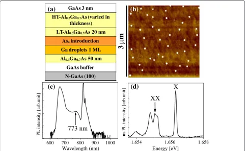
GaAs DE QD samples were grown by a molecular beam epitaxy (MBE) system. Figure 1a shows a full sample struc-ture, with low-density GaAs DE QDs (approximately 4 QDs/μm2) on an Al0.3Ga0.7As/GaAs substrate, with a vari-able thickness Al0.3Ga0.7As cap layer. After deoxidation at approximately 600°C under As4 and Al0.3Ga0.7As/GaAs buffer layer growth, formation of low-density Ga droplets was tested to predict the diameter, height, and density of GaAs DE QDs. Figure 1b indicates an AFM image of low-density GaAs DE QDs used in the full structure of Figure 1a. The As4flux with beam equivalent flux of 1 × 10⁻⁵Torr during 60 s was introduced on low-density Ga liquid droplets, as in Figure 1b, near room temperature. After As4 injection, a 20-nm-thick Al0.3Ga0.7As (LT-Al0.3Ga0.7As) layer covered low-density GaAs DE islands at near room temperature, to retain the shape of GaAs DE islands. Then, an additional Al0.3Ga0.7As layer (HT-Al0.3Ga0.7As) was grown, increasing the substrate temperature up to approximately 580°C. The thickness
3
µ
m
(b)
GaAs 3 nm
HT-Al0.3Ga0.7As (varied in
thickness)
LT-Al0.3Ga0.7As 20 nm
As4introduction
Ga droplets 1 ML
Al0.3Ga0.7As 50 nm
GaAs buffer
N-GaAs (100)
600 700 800 900 1000
PL intensity [arb.unit]
Wavelength (nm)
773 nm
1.654 1.656 1.658
m
-PL intensity [arb.unit]
Energy [eV]
X
XX
(d)
(c)
[image:2.595.57.539.388.684.2](a)
of the additional Al0.3Ga0.7As layer was varied and of 2, 25, 50, and 85 nm (the total thickness of Al0.3Ga0.7As was 22, 45, 70, 105 nm, respectively). The top of Al0.3Ga0.7As-capped samples was covered by 3-nm-thick GaAs. Rapid thermal annealing (RTA) was per-formed at 850°C for 240 s with ambient Ar, to improve crystallinity of GaAs DE islands. A macro-PL andμ-PL at low temperature (12 ~ 16 K) were measured by 532-nm laser to verify the formation of quantum structures, depending on the thickness of capping layers, and exci-tonic states of low-density GaAs DE QDs.
Results and discussion
Figure 1b shows an AFM image of low-density GaAs DE QDs obtained by a change of growth conditions, such as growth temperature, Ga flux, and Ga coverage. Low-density GaAs DE QDs in Figure 1b showed 81.6 ± 9.5 nm in diameter, 14.7 ± 1.7 nm in height, and 4.4 QDs/μm2. Typically, in our case, after injection of As4, the change of GaAs DE QDs in density and diameter was negligible, compared with those of the Ga droplets. However, the height of the GaAs DE QDs was approximately two times larger than that of the Ga droplets. The height of Ga drop-let is in the range of 7 ~ 8 nm. Here, the authors should point out that the shape of the GaAs DE QDs is not iden-tical when they are grown on the surface and buried in the AlGaAs matrix. In the case of GaAs DE QDs of reference [7], the size of GaAs DE QDs on the surface was approxi-mately 12-nm height and approxiapproxi-mately 60-nm width and found that approximately 9-nm height and approximately 35-nm width when they were placed in the AlGaAs matrix. Furthermore, the effective size of GaAs DE is add-itionally reduced due to post-thermal annealing/intermix-ing and finally gives us the low-temperature PL peaks around 1.70 ~ 1.80 eV. Considering larger size of the GaAs DE QDs in this experiment as a starting size on the sur-face, the PL peaks in Figure 1c around 1.60 eV (approxi-mately 0.773 nm) are attributed to the GaAs DE QDs after AlGaAs capping and post-annealing/intermixing.
A macro-PL of low-density GaAs DE QDs with 105-nm Al0.3Ga0.7As cap layer at 12 K was observed after RTA. Low-density GaAs DE QDs were formed by As4injection on Ga droplets of Figure 1b. The emission of low-density GaAs DE QDs was verified at approximately 773 nm in Figure 1c. Based on the result of macro-PL, aμ-PL of low-density GaAs DE QDs (approximately 4 QDs/μm2) at 16 K was performed. Figure 1d shows exciton (X)/biexci-ton (XX) behavior in the range of 1.654 to 1.657 eV. Ex-citon and biexEx-citon behavior can be characterized by the value of biexciton binding energy [17]. A few studies have reported 3 to 5 meV for the biexciton binding energy of GaAs QDs [17,18]. The diameter of QDs in such studies was less than approximately 50 nm. In our case, the biex-citon binding energy was approximately 1.2 meV, and the
diameter of QDs was 70 ~ 90 nm. The relatively small biexciton binding energy for the present QDs would be at-tributed to a large size of QDs, since an increase of radius of QDs reduces biexciton binding energy [19]. For the ex-citon peak, a full width at half maximum (FWHM) showed approximately 136μeV. Mano et al. have reported that narrow linewidth around 35 μeV has been observed from an emission of a single GaAs DE QD [6]. Since the value of FWHM depends on the local environment, re-gardless of QD emission energy, this larger FWHM value could be reduced by improving the quality of the barrier in QD structure, for instance, by annealing during growth [6,20]. The optical properties of low-density GaAs DE QDs of the authors’sample are covered in detail at the other articles of reference [21].
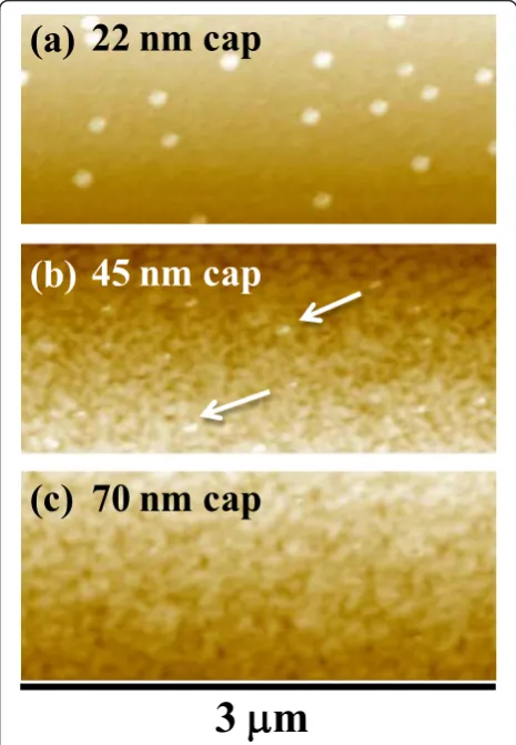
[image:3.595.305.538.360.696.2]For low-density GaAs DE QDs, as shown in Figure 1c, d, the surface of Al0.3Ga0.7As-capped GaAs DE QDs was investigated by AFM. Figure 2 indicates AFM images of low-density GaAs DE QDs, with a 22, 45, and 70-nm capping. At 22- and 45-nm capping, the position of low-density GaAs DE QDs was observed. Flat and uniform
Figure 2AFM images (3μm × 3μm) of a surface. (a)22-nm,
AFM surfaces were found with the Al0.3Ga0.7As capping thickness of 70 and 105 nm (not shown here).
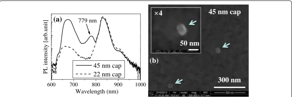
For low-density GaAs DE QDs with 22- and 45-nm cap-ping, a macro-PL at a low temperature (approximately 12 K) was measured, to verify an emission of low-density GaAs DE QDs, as shown in Figure 3a. Low-density GaAs DE QDs with a 45-nm-thick capping layer showed an emis-sion at approximately 779 nm. However, 22-nm-capped GaAs DE QDs had no emission peak of QDs. An emission at approximately 779 nm for low-density GaAs DE QDs with a 45-nm capping matches the macro-PL result of 773-nm emission in Figure 1c. The PL bands around 660 and 830 nm shown in Figures 1c and 3a are attributed to Al0.3Ga0.7As and GaAs, respectively. The larger intensity of the PL band near 660 nm is found with the thicker AlGaAs capping layer in Figure 3a.
Figure 3b shows a SEM image of low-density GaAs DE QDs with a 45-nm cap, and arrows point out the position of GaAs DE QDs. Since SEM is widely used for a post-fabricating process, such as electron-beam lithography to form special structures like mesa or micro-pillar, it is signifi-cant that the position of QDs is observed on a SEM image. Furthermore, the wavelength of 779 nm is suitable for pick-ing up appropriate spick-ingle QDs in conventional cathode-luminescence apparatus, usually connected to modern SEM. The noteworthy result is that the density of GaAs DE QDs with a 45-nm-thick Al0.3Ga0.7As capping on the SEM image of Figure 3b corresponds to the density of Ga DE QDs (ap-proximately 4 QDs/μm2) on the AFM image of Figure 1b. No change of density of QDs from droplets is due to i) im-mediate injection of As4at near room temperature after Ga droplet growth and ii) suppression of Ostwald ripening con-siderably depending on growth temperature and growth interruption time [22]. This result mentions that prediction of the density of GaAs DE QDs at the step of Ga droplet formation is reliable, even after capping.
Here, it should be pointed out that the author cannot expect the optical properties of GaAs DE QDs with thin AlGaAs capping layer (45 nm) are the identical to that of GaAs DE QDs with 105-nm-thick AlGaAs capping layers. There will be the increasing effect of the surface as the thickness of AlGaAs decreases. The authors ar-gued that the confinement of carrier by GaAs DE QDs was found as thin as 45 nm of AlGaAs capping by macro-PL, which was useful to plasmatic coupling appli-cation and can be locatable in SEM. In the near future, the authors will focus on the effect of thinness of cap-ping on the individual QDs withμ-PL.
Conclusions
In conclusion, 45-nm Al0.3Ga0.7As-covered GaAs DE QDs (approximately 4 QDs/μm2) have been retrievable on a SEM and an AFM. Low-density GaAs DE QDs with a 45-nm-thick capping layer showed the emission of a macro-PL at approximately 779 nm. For fully capped GaAs DE QDs (105-nm Al0.3Ga0.7As cap), a macro-PL shows an emission peak at approximately 773 nm, and an exciton/biexciton peak was verified at approximately 1.656 and approximately 1.655 eV, respectively, by μ-PL. Observation of these low-density GaAs DE QDs, that is, retrieving of an optically ac-tive single QD on the capped surface, would be of consider-able impact to the mass production of devices using a single QD.
Competing interests
The authors declare that they have no competing interests.
Authors’contributions
EHL, IKH and JDS grew the samples. EHL, SKC, and JSK carried out the structural and optical measurements. FL, SH, AF, and MK carried out the micro-PL for measuring optical properties. JDS participated in its design and coordination and helped to draft the manuscript. All authors read and approved the final manuscript.
600 700 800 900 1000
779 nm
45 nm cap
22 nm cap
PL intensity [arb.unit]
Wavelength (nm)
(a)
50 nm
(b)
4
[image:4.595.58.539.89.249.2]300 nm
45 nm cap
Acknowledgements
This work was mainly supported by the Ministry of Education, Science and Technology through the Global Research Laboratory Program and by collaboration within the Center for Photonics and Nanostructures, KIST-CNRS International Associated Labs. The authors in KIST acknowledge the partial support from the KIST institutional program.
Author details
1Center for Opto-Electronic Convergence Systems, Korea Institute of Science and Technology, Seoul 136-791, South Korea.2Institute of Physics and Applied Physics, Yonsei University, Seoul 120-749, South Korea.3Technische Physik, Universität Würzburg, Am Hubland, 97074 Würzburg, Germany. 4Department of Physics, Yeungnam University, Gyeongsangbuk-Do 712-749, South Korea.
Received: 27 August 2014 Accepted: 17 February 2015
References
1. Michler P, Kiraz A, Becher C, Schoenfeld WV, Petroff PM, Zhang L, et al. A quantum dot single-photon turnstile device. Science. 2000;290:2282. 2. Cavigli L, Abbarchi M, Bietti S, Somaschini C, Sanguinetti S, Koguchi N, et al.
Individual GaAs quantum emitters grown on Ge substrates. Appl Phys Lett. 2011;98:103104.
3. Jo M, Mano T, Sakoda K. Two-step formation of gallium droplets with high controllability of size and density. Cryst Growth Des. 2011;11:4647. 4. Liang BL, Wang Zh M, Lee JH, Sablon K, Mazur Yu I, Salamo GJ. Low density
InAs quantum dots grown on GaAs nanoholes. Appl Phys Lett. 2006;89:043113.
5. Ishikawa T, Nishimura T, Kohmoto S, Asakawa K. Site-controlled InAs single quantum-dot structures on GaAs surfaces patterned by in situ electron-beam lithography. Appl Phys Lett. 2000;76:167.
6. Mano T, Abbarchi M, Kuroda T, Mastrandrea CA, Vinattieri A, Sanguinetti S, et al. Ultra-narrow emission from single GaAs self-assembled quantum dots grown by droplet epitaxy. Nanotechnology. 2009;20:395601.
7. Moon P, Lee JD, Ha SK, Lee EH, Choi WJ, Song JD, et al. The effect of post-growth thermal annealing on the emission spectra of GaAs/AlGaAs quantum dots grown by droplet epitaxy. Phys Status Solidi Rapid Res Lett. 2012;6:445.
8. Dousse A, Lanco L, Suffczyński J, Semenova E, Miard A, Lemaître A, et al. Controlled light-matter coupling for a single quantum dot embedded in a pillar microcavity using far-field optical lithography. Phys Rev Lett. 2008;101:267404.
9. Nogues G, Merotto Q, Bachelier G, Lee EH, Song JD. Fabrication and tuning of plasmonic optical nanoantennas around droplet epitaxy quantum dots by cathodoluminescence. Appl Phys Lett. 2013;102:231112.
10. Badolato A, Hennessy K, Atatüre M, Dreiser J, Hu EL, Petroff PM, et al. Deterministic coupling of single quantum dots to single nanocavity modes. Science. 2005;308:1158.
11. Hennessy K, Badolato A, Winger M, Gerace D, Atatüre M, Gulde S, et al. Quantum nature of a strongly coupled single quantum dot-cavity system. Nature. 2007;445:896.
12. Mano T, Koguchi N. Nanometer-scale GaAs ring structure grown by droplet epitaxy. J Cryst Growth. 2005;278:108–12.
13. Mano T, Watanabe K, Tsukamoto S, Koguchi N, Fujioka H, Oshima M, et al. Nanoscale InGaAs concave disks fabricated by heterogeneous droplet epitaxy. Appl Phys Lett. 2000;76:3543–5.
14. Mano T, Kuroda T, Sanguinetti S, Ochiai T, Tateno T, Kim JS, et al. Self-assembly of concentric quantum double rings. Nano Lett. 2005;5:425–8. 15. Yamagiwa M, Mano T, Kuroda T, Tateno T, Sakoda K, Kido G, et al.
Self-assembly of laterally aligned GaAs quantum dot pairs. Appl Phys Lett. 2006;89:113115.
16. Gazzano O, Michaelis de Vasconcellos S, Gauthron K, Symonds C, Bloch J, Voisin P, et al. Evidence for confined tamm plasmon modes under metallic microdisks and application to the control of spontaneous optical emission. Phys Rev Lett. 2011;107:247402.
17. Ha SK, Song JD, Kim SY, Lee JI, Bounouar S, Dang LS, et al. Optical characterization of the excitonic states in low-density droplet GaAs quantum dots for single photon sources. J Korean Phys Soc. 2011;58:1330–3.
18. Abbarchi M, Troiani F, Mastrandrea C, Goldoni G, Kuroda T, Mano T, et al. Spectral diffusion and line broadening in single self-assembled GaAs/AlGaAs quantum dot photoluminescence. Appl Phys Lett. 2008;93:162101. 19. Hu YZ, Koch SW, Lindberg M, Peyghambarian N, Pollock EL, Abraham FF.
Biexcitons in semiconductor quantum dots. Phys Rev Lett. 1990;64:1805. 20. Kuroda K, Kuroda T, Watanabe K, Mano T, Kido G, Koguchi N, et al.
Distribution of exciton emission linewidth observed for GaAs quantum dots grown by droplet epitaxy. J Lumin. 2010;130:2390–3.
21. Tighineanu P, Daveau R, Lee EH, Song JD, Stobbe S, Lodahl P. Decay dynamics and exciton localization in large GaAs quantum dots grown by droplet epitaxy. Phys Rev B. 2013;88:155320.
22. Heyn C, Stemmann A, Schramm A, Welsch H, Hansen W, Nemcsics Á. Regimes of GaAs quantum dot self-assembly by droplet epitaxy. Phys Rev B. 2007;76:075317.
Submit your manuscript to a
journal and benefi t from:
7Convenient online submission
7Rigorous peer review
7Immediate publication on acceptance
7Open access: articles freely available online
7High visibility within the fi eld
7Retaining the copyright to your article