Rochester Institute of Technology
RIT Scholar Works
Theses
Thesis/Dissertation Collections
2-1-1979
A Synchronous Data Compression System
Joseph Calcagno
Follow this and additional works at:
http://scholarworks.rit.edu/theses
This Thesis is brought to you for free and open access by the Thesis/Dissertation Collections at RIT Scholar Works. It has been accepted for inclusion
in Theses by an authorized administrator of RIT Scholar Works. For more information, please contact
.
Recommended Citation
Approved by:
A SYNCHRONOUS DATA COMPRESSION SYSTEM
by
Joseph S. Calcagno
A Thesis Submitted
in
Partial Fulfillment
of the
Requirements for the Degree of
MASTER OF SCIENCE
in
Electrical Engineering
Prof. George A. Brown
(Thesis Advisor)
Prof.
E.
R.
Salem
Prof. George
L.
Thompson
Prof.
Harvey E. Rhody
(Department Head)
DEPARTMENT OF ELECTRICAL ENGINEERING
COLLEGE OF ENGINEERING
ROCHESTER INSTITUTE OF TECHNOLOGY
ROCHESTER, NEW YORK
PREFACE
A
unique sequence of events madethe
subject ofthis
thesis
possible.In
June
of1974
my
supervisor(at
Xerox
Corporation)
asked meto
develop
a specificationfor
a general purposedata
acquisition system(D.A.S.).
This
was a
low priority
task
and required about six months of sparetime
to
complete.The
D.A.S.
system was not continuedbecause
ofhigher
priority
work.Because
ofmy
interest in D.A.S.
systems,I
continuedto
develop
the
system
design
onmy
own.In
July
of1975
I
transferred to
a newdepartment.
An
engineerin
this
department
wasin
the
process ofordering three
chart recordersto
be
usedfor
a series ofexperiments.After showing him
the
advantages ofusing my
D.A.S.,
he
cancelledhis
order and gave methe
go-aheadto
build
the D.A.S.
Since
this
was notmy
primary
assignment,I
gotmy
supervisor's approvalto
undertakethis task
onthe
conditionthat
it
wouldbe
operationalin four
months, wouldbe
100%
designed, built,
anddebugged
by
me, and would notinterfere
withmy
primary
activities.The
D.A.S.
was made operationalby
December
1975,
but
requiredmany
nights and weekends.I
enteredthe
Master's degree
program(M.S.
E.E.)
in
the
winter quarter of1975.
Professor George A.
Brown
agreedto
be
my
lead
advisorfor
athesis
onthe
data
acquisition system andthe thesis
was startedin March 1977.
I
wishto thank Professor
George
Brown
for his
guidance and assistanceduring
the
18
monthsthat
I
worked onthe thesis.
I
also wishto thank
Dr.
Swaminathan
Madhu
whois
the Director
ofGraduate Programs for
the
College
ofEngineering
atthe Rochester
Institute
ofTechnology
for allowing
meto
usethe
D.A.S.
asthe
subjectfor my thesis.
I
wishespecially to thank my
wifefor her
support,
encouragement, and sacrifice.A
specialthanks
goesto my
sisterMarge Hodges for
typing
the thesis.
Last
but
notleast
aremy two
childrenDavid
andJanet,
who understoodwhy their
father's
presence was so scarceduring
the
preparation ofthis thesis.
ABSTRACT
This
thesis
discusses
in detail
the
steps requiredfor
the
design
of a general purposeData
Acquisition
System
(D.A.S.).
This
D.A.S.
is
called aSynchronous
Data
Compression
System
(S.D.C.S.)
because
of some specialfeatures.
The S.D.C.S.
is
designed
to
acceptdata in analog
ordigital
form.
A
simple control panelinterface
is
developed,
and areas of primeinterest
such asinput/output interface
control, analog-to-digital conversion,data
compression,and
data
sampling
modes arediscussed in detail.
?The
primary
logic
type
usedfor
the
S.D.C.S.
is
the
CMOS
type
4000
Series
whichwas
developed
by
R.C.
A.
TABLE OF CONTENTS
Page
LIST OF
TABLES
vLIST OF FIGURES
viLIST OF SYMBOLS
x1.
INTRODUCTION
1
2.
HISTORICAL
REVIEW
2
3.
DATA
ACQUISITION
SYSTEM DEVELOPMENT
4
3.1
Development
ofthe
System Specification
4
3.2
Choosing
Between Various
Sub-System
Design
Approaches
....17
3.2.1
Selection
ofthe
Data Compression
Control
Sub-System
.21
3.2.2
Selection
ofthe
Control
Panel
Interface
Sub-System
.33
3.2.3
Selection
ofthe
Data
Channel
Monitor
Sub-System
...42
3.2.4
Selection
ofthe
Data Tolerance
Memory
Sub-System
. .45
3.2.5
Selection
ofthe
Data Compression
Rate
andSample
Rate Sub-System
48
3.2.6
Selection
ofthe
A/D
Conversion
Sub-System
54
3.2.7
Selection
ofthe
Data
Channel
Interface
Sub-System
. .62
3.2.8
Selection
of aMethof
for
BCD
Conversion
andfor
Transmission
ofthe
Floating
Decimal
Point
74
4.
SYSTEM TIMING AND
CONTROL
85
4.1
Primary
System
Timing
85
4.2
Secondary
System
Timing
89
5.
SUB-SYSTEM
DESIGN
92
5.1
Data Channel
Monitor
Control
92
5.2
Data
Compression Rate
andSample Rate Control
101
5.3
Data Compression Sub-System
103
5.4
The
A/D
Conversion Sub-System
126
5.5
Line
Printer
Sub-System
146
5.6
Data Channel
Input
-Interface
Control
152
5.7
Miscellaneous
System Functions
154
6.
RESULTS
156
7.
SUMMARY
166
APPENDIX
A
-REFERENCES
167
LIST
OF TABLES
TABLE
Page
3.1
MATRIX MODEL SELECTION
CHART
15
3.2
MATRIX ASCII CODE
75
3.3
PRINT FORMAT FOR TIME AND DATA
77
5.1
FIVE COMPARE
CONDITIONS
110
5.2
FINAL STAGES
OF
SIGNAL H
115
5.3
(a)
PRINTER
MUX
SELECTION CODES
151
LIST
OF FIGURES
Figure
Page
3.1
FIRST-LEVEL
BLOCK DIAGRAM
OF THE S.D.C.S
18
3.2
SECOND-LEVEL
BLOCK DIAGRAM
OF THE
S.D.C.S
19
3.3
SUB-SYSTEM
COMPONENTS
OF THE S.D.C.S
20
3.4
DATA TOLERANCE
WINDOW EXAMPLE
23
3.5
DATA
COMPRESSION
WITH
PROGRAMMABLE AMPLIFIER
...26
3.6
DATA COMPRESSION WITH BCD RATE MULTIPLIER
28
3.7
DATA COMPRESSION USING TIME-SHARED
D/A,
ADD/SUB.
LOGIC,
AND COMPARITORS
30
3.8
DATA
COMPRESSION WITH
AN ALL-DIGITAL SOLUTION
31
3.9
CONTROL PANEL
LAYOUT
34
3.10
(a)
MAXIMUM-WIRE
INTERFACE TO
LED DISPLAY
35
3.10
(b)
MULTIPLEXED INTERFACE TO
THE 7-SEGMENT DATA DISPLAY
. .38
3.11
FINAL
MULTIPLEXER
DESIGN
41
3.12
DATA CHANNEL MONITOR
CONTROL
WITH BINARY
COUNTERS
. .43
3.13
DATA
CHANNEL MONITOR CONTROL WITH
BCD
COUNTERS
....44
3.1.4
DATA
TOLERANCE
MEMORY
.47
3.15
SAMPLE RATE
SUB-SYSTEM
49
3.16
SAMPLE RATE
REGISTER
NO.
1
50
3.17
SAMPLE RATE
REGISTER
NO.
2
51
3.18
SAMPLE RATE
REGISTER NO.
3
53
3.19
ONE
A/D CONVERTER
CYCLE
56
3.20
V/F
CONVERTER SUB-SYSTEM
59
3.21
DUAL SLOPE
A/D
CONVERTER SUB-SYSTEM
61
3.22
BASIC
MODULE
INTERFACE
64
LIST OF FIGURES
Figure
Page
3.23
(a)
MODULE-SIDE
ANALOG
MULTIPLEXING
65
3.23
(b)
SYSTEM-SIDE ANALOG
MULTIPLEXING
65
3.24
(a)
MULTIPLEXED
PARALLEL DIGITAL
DATA
66
3.24
(b)
MULTIPLEXED
SERIAL DIGITAL DATA
66
3.25
SERIALLY
MULTIPLEXED DIGITAL DATA
.68
3.26
MODULE
CONNECTOR SIGNALS
70
3.27
DUAL
AC/DC
VOLTMETER CHANNELS
73
3.28
(a)
PRINT MULTIPLEX
SOLUTION
NO.
1
80
3.28
(b)
TYPICAL
DATA
FORMAT
80
3.29
MULTIPLEX
SEQUENCE
FOR
C, D.P.,
B,
A
81
3.30
MULTIPLEX SOLUTION
NO.
2
83
4.1
PRIMARY
SYSTEM
TIMING
87
4.2
MULTIPLEXED
AND
ENCODED
CHANNEL
SELECT
90
5.1
BLOCK DIAGRAM OF
CHANNEL
NUMBER
SELECTION AND CHANNEL
TOLERANCE MEMORY
CONTROL
93
5.2
PRIMARY
TIMING,
COMPARE,
AND
MEMORY
TOLERANCE SUB-SYSTEMS
.95
5.3
TOLERANCE MEMORY TIMING
97
5.4
DATA MONITOR MULTIPLEXER
100
5.5
SAMPLE
RATE
SELECTION
LOGIC
102
5.6
BASIC LIMIT COMPARE FUNCTIONS
104
5.7
LIMIT COMPARE STEPS
105
5.8
FUNCTIONAL BLOCK DIAGRAM
OF
UPPER/LOWER
LIMIT DETECTION
. .107
5.9
SERIAL
ADDER AND TIMING
109
LIST OF FIGURES
Figure
Page
5.10
LOGIC DESIGN FOR
UPPER/LOWER
LIMIT DETECTION
112
5.11
TIMING FOR
UPPER/LOWER LIMIT
DETECTION LOGIC
113
5.12
MODIFICATION
OF AA
COUNTER
117
5.13
BINARY COUNTER
FOR DATA
VALUE A
WITH
"INH-0"ADDITION
119
5.14
LIMIT
COMPARE
LOGIC
121
5.15
LIMIT COMPARE
TIMING
122
5.16
FINAL
DATA
COMPRESSION
SUB-SYSTEM
125
5.17
BLOCK
DIAGRAM
OF A/D CONVERSION SUB-SYSTEM
127
5.18
ANALOG MUX
AND VOLTAGE
FOLLOWER
129
5.19
ABSOLUTE
VALUE
CIRCUIT
131
5.20
A/D CONVERSION
SUB-SYSTEM
132
5.21
FUNCTIONAL
DIAGRAM
OF A/D CONVERSION
134
5.22
DUAL
SLOP
A/D CONVERSION WAVEFORMS
134
5.23
MCI
505
SYSTEM TIMING DIAGRAM
136
5.24
DIGITAL SUB-SYSTEM TIMING FOR
A/D CONVERTER
137
5.25
A/D COMPARE TIMING
141
5.26
LINE PRINTER SUB-SYSTEM
147
5.27
ASCII CHARACTER TIMING
148
5.28
DATA CHANNEL
I/O
CONTROL
153
5.29
MISCELLANEOUS FUNCTIONS
155
6.1
S.D.C.S.,
FRONT VIEW
160
LIST OF FIGURES
Figure
Page
6.3
S.D.C.S.,
TOP-BACK VIEW
162
6.4
S.D.C.S.,
BACK VIEW
163
6.5
S.D.C.S.
AND LINE
PRINTER
.164
LIST
OF SYMBOLS
SYMBOL
N
D
E
VD
VR
'f
Vcc
Pt
f
Tl
T2
Rf
RIN
I
'o
T
Columns
perline.
Data
value.Compare
tolerance.
Analog
data
value.Analog
value equalto
.075% offull
'scale.
LED
digit
segment current.Logic
supply
voltage of +5VDC.
Power
dissipation
of oneLED
seven-segmentdigit.
Clock
for A/D
converter.Period
off
.Total
conversiontime.
Feedback
resistance.Input
resistance.Charge
current.Offset
Current
1.
Introduction
This
thesis
describes
the
design
and construction of a generalpurpose
Data
Acquisition
System
(D.A.S.)
which canbe
usedto
monitor
analog
anddigital
data.
The development
ofthe D.A.S.
is
dependent
uponexisting
hardware,
andthe
latest CMOS integrated
circuits
in
the
4000, 4500,
and74C00 families.
Other integrated
circuit
types
are used wherehigher
power orswitching
speeds arerequired.
The D.A.S.
is designed
to
acquiredata
in
a synchronous manner sothat
data
plots canbe
moreeasily
obtained automatically.Print-out
of
data
is
accomplishedin
any
offour
data
acquisition modes.The
primary
(and
mostuseful)
modeis
the
"data
compression"mode which
is
explainedin
paragraph5.3.
Because
ofthe two
important features
of synchronous
data
acquisition and ofdata
compression,
this
systemis
described
as aSynchronous
Data Compression
System
(S.D.C.S.).
The
subject ofthis
thesis
has
been
organizedin four
parts.The
first
part(para.
3.1)
develops the
system specification.The
second part
(para.
3.2)
develops
two
or more solutionsto
eachsub-system requirement and selects
the
best
solution.The
third
part
(para.
4)
develops
the primary
andsecondary
systemtiming,
Historical
Review
Data
acquisition associated withengineering
development
of componentsand products
has
accelerateddramatically
sinceits
primitivebeginning
which
essentially
startedduring
the early
1900's.
Companies
such asGeneral
Electric, Westinghouse,
andRCA
wereamong the
pioneersin
this
field.
Data
acquisition requirestransducers to
convert a physical phenomena ofinterest into
aneasily
measured electrical signal.Transducers
developed
in step
withthe necessity to
measurenewly
discovered
phenomena.It is
not
surpising
to
note,therefore,
that
long
before
there
wasany
suchthing
as asteady
electric current,that
is before
1800,
attempts werebeing
madeto
estimatethe
strength of a magnet andthe
value of a staticpotential .
Today
there
areliterally
hundreds
oftransducers
usedfor
measuring
temperature,
force,
time,
pressure,flow,
velocity,acceleration,
humidity,
viscosity, and
literally
hundreds
of other physical measurements.Data
acquisition, evaluation, reduction, and presentation
has become
moresophisticated as
the
data
acquisition systems evolvedfrom
the
vacuumtube,
to
the
transducer,
then to the
integrated
circuit.The
mostsophisticated systems
employ
computers and massdata
storage.The
microprocessoris
rapidly replacing the
medium sizedata
acquisitionsystem
in
the
laboratory.
Many
companies areintroducing
microprocessor-based
data
acquisition systems.Tailored
data
acquisition systems canbe
Motorola,
Digital
Equipment, Pro-Log
orZilog,
with ananalog
I/O
board from
companies such asBurr-Brown,
Analog
Devices,
Datel
andAnalogic.
The
addition oftransducers,
control panelinterface,
storage
-such as
disc
or magnetictape,
and a printoutdevice
willprovide a
full
-fledged,data
acquisition system.Many
companies areintroducing
microprocessor-baseddata
acquisitionsystems which require
only the
addition oftransducers
and an output3.
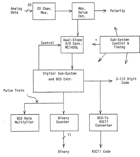
Data Acquisition System
Development
A data
acquisition systemhas little
valueif it does
notsatisfy the
requirements of
the
user.In
this
case,the
useris
testing
an electromechanical piece of equipment and
is
monitoring
analog
anddigital
forms
ofdata from it.
He is
primarily interested
in instantaneous
printout of alldata for
visual examination.3.1
Development
ofthe
System Specification
The Synchronous Data
Compression
System
(S.D.C.S.)
requirementsare as
follows:
3.1.1
Data
Input
The
system shallbe designed
to
acceptanalog
anddigital
data.
The analog
signalconditioning
electronics shallbe
mounted on a printed circuit
board
and willbe
located
in
the
bottom-half
ofthe
S.D.C.S.
chassis.Interface
requirements
for
digital
data
channels can alsobe
mounted on aninput
printed circuitboard.
3.1.2
Data Output
A line
printer shallbe
usedto
obtain a printout ofthe test
data.
The
control panel can alsobe
usedto
monitor a selecteddata
channel .3.1
.3Print Format
3.1.4
Data Sample
andPrint Rate
All data
channels willbe
sampled at a rate which shall notexceed
the
maximum print rate.The
maximum print rateis
dependent
uponthe
line
printer which willbe
selectedlater.
3.1.5
Data
Compression
In
this
mode ofoperation,
data
willbe
printedonly
if
one(or
more)
data
channel(s)
exceeds a specified percentage ofchange with respect
to the
last
printeddata
value(s).Data
compression
is
explainedin detail
in Section
3.2.1,
Page 21
thru 32.
3.1.6
Selectable
Data
Rate
In
this
mode of operation,time
and alldata
channelscan
be
printedin
oneline
atany
one ofthe
following
fixed
rates:a.
One line
per second.b.
One line
per10
seconds.c.
One line
per minute.d.
One line
per10
minutes.The
S.D.C.S.
can operatein
the Data
Compression
mode,in
the fixed
rate mode, orin
both
modes simultaneously.3.1.7
Manual
Print Request
One line
ofdata
shallbe
printed whenthe
PRINT REQUEST
3.1.8
Automatic
One line
ofdata
shallbe
printed when adigital
channelhas
validdata.
This
can occur atthe
maximum print ratewhich will
be
determined
later.
3.1.9
Control
Panel
Features
a.
Channel
Monitor
Capability
The
control panel shall containLED
digits
to
display
the
selecteddata
channel number,data
compressiontolerance,
anddata
value,including
sign.The
monitorfunctions
shall operate asfollows:
1.
Channel
Number
Selection
andDisplay
Two
touch
buttons
are availablefor
incre
menting
ordecrementing
the
channel number ata rate of
two
counts per second.Channel
0
is
usedto
display
the
real-time clock.Channel
number
1
thru
N
shall monitordata
channels1
thru
N
respectively.Channels
N+l
,N+2,
andN+3
shall contain reference voltagesfor
calibration
ofthe
A/D
converter.2.
.Channel
Data
Display
The
selected channeldata
value andpolarity
shall
be
displayed
onL.E.D.
digits.
Analog
channels are updated
every
0.5
seconds.When
a
digital
channelis
selected,
the
display
will3.
Data
Channel
Tolerance
Display
The
tolerance
ofthe
selecteddata
channel willbe
displayed
ontwo
L.E.D.
digits.
Two
touch
buttons
are availablefor
incrementing
ordecrementing
the tolerance
ofthe
selectedchannel at a rate of
two
percentage counts persecond.
The
tolerance
rangefor
each channelis
1
thru
15
percent and99
(or
OFF)
percent.When
poweris
turned on,
all storeddata
tolerances
shallbe initialized
to
99
percent.b.
Data Compression Sample Rate
At
this
time
anarbitrary
number offour
switchesshall
be
usedfor selecting
one of ourdata
compression rates.
The data
compression rates willbe
selected whenthe
maximum print rateis deter
mined.
The four
switches shallbe
momentary
andmade
to
function
asinterlock
switches.An L.E.D.
lamp
shallbe
located
above each switchfor
the
purpose of
indicating
the
selecteddata
compressionrate.
When
poweris
turned on,
alldata
compressionrate
indicators
willbe
turned
off.c.
Fixed Data Sample Rate
A
touch-button switchis
availablefor
selection ofeach of
the
data
sample rates.The
four
requiredinterlock
switches.An
L.E.D.
lamp
shallbe located
above each switch
for
the
purpose ofindicating
the
selected
data
sample rate.The S.D.C.S.
shallbe
made
to
operatein
the data
compression mode only,in
the
data
sample rate mode only, orin
both
modessimultaneously.
When
poweris
turned on, alldata
rate
indicators
willbe
off.d.
Data Request
One line
ofdata
shallbe
printed whenthe DATA
REQUEST
switchis
activated.An
L.E.D.
lamp
shallbe
located
abovethis
switch and shallilluminate
when
the
switchis
activated.e.
Control
Panel
Lock Switch
A
LOCK
switch shallbe
usedto
prevent accidentalactivation of
the
Data
Compression
andData
Sample
Rate
switches.An L.E.D.
lamp
shallbe located
above
the
LOCK
switch and shallilluminate
whenthe
LOCK
switchis
activated.When
poweris
turned on,
the
LOCK
switch shallbe
activated.f.
Printer
ON/OFF Switches
Activation
ofthe PRINTER
ON
switch shall enabledata
transfer
to the
line
printer.Activation
ofthe
PRINTER OFF
switch shallinhibit data
transfer
to the
line
printer.An L.E.D.
lamp
shallbe located
above each switch
to
indicate
which switchis
activated.When
poweris
turned on, the PRINTER
OFF L.E.D.
lamp
shall
be illuminated.
g.
Control
Panel
Switches
The
operator shallbe
allowedto
changethe
channelnumber,
data
tolerance
memory,data
compression ordata
sample rates whilethe
printeris
on(or
off)
without
causing
irregular
orfalse
printout.Activa
tion
ofthe
PRINTER OFF
switch shall not causefalse
or partial printout.
3.1.10
Common I/O Interface
The I/O
interface
to the analog
anddigital
printedcircuit
boards
shallbe designed
to
allowany
printedcircuit
board type to
plug into
any
connectorlocation.
3.1.11
Data
Channel
Inputs
The
following
factors
willdetermine
the
number ofdata
channels:
a.
Selection
of a standard(commonly
used)
type
ofb.
The
requirementto
printtime
and alldata
channels
in
oneline.
c.
The
number of characters required perdata
channel.
This is dependent
uponthe
following
factors:
1.
Data
resolution required.2.
Requirement
ofpolarity indication
anddecimal
point.3.
Separation
ofdata
channelsby
atleast
oneletter
space.4.
Special
characters,
if
required.d.
The
type
ofhardware
whichis
availablefor data
channel plug-in modules.
e.
The
number ofdata
channels per plug-in module.3.1.12
Analog
Data Conversion
Accuracy
The
primary
aim ofthe
Synchronous Data Compression
System
(S.D.C.S.)
is
to
monitorthose types
of systemswhere
high
accuracies are not required.Using
present-day
components, adata
system with an overallaccuracy
of
0.1
to
.15 percent offull
scale shouldbe
considered.This
includes
signal conditioning,multiplexing,
andto-digital
(A/D)
conversion.Polarity
is
adesirable feature
and should,therefore,
be
included.
Measurements
such as +D.C.
volts,temperature,
deceleration
anddifferential
pressure areonly
afew
examples of
bipolar
measurements.Resolution
andpolarity
requirementsdictate
that
the
A/D
converter must
have
anaccuracy
of +.05percent,
+1
bit,
andanalog conditioning
would alsohave
a +^.05 percent accuracy.The A/D
converter mustthen
have
atleast
an11
bit
binary
or a3-1/2
digit
BCD
resolution.In
eithercase, printout will
be
a3-1/2 digit
signed value withdecimal
point.Considering
that
data
printout shouldhave
at
least
oneletter
spacebetween data
channels,
atotal
of seven columnsis
required perdata
channel.The
logic
design
canbe
simplifiedby
using the
same number ofcolumns
for
time
anddata.
The
equationfor
the
number ofdata
channels(X)
which canbe
printedin
oneline
ofN
columns
is
then:
7
(X
+1)
=N
or:
X
=(N/7)
-1
N
=80
for
the
standard80
column printer and:X
=(80/7)
-1
=10.43
=10 data
channels.For
a standard132
column printer:X
=(132/7)
-1
=17.86
=17 data
channelsHardware is
another consideration.Vector Corporation
makes a
19 inch
wide card cage which canhold
eight2.0
inch
wide card modules orten
1.6 inch
wide card modules.A
card moduleis
a metalbox
whichhouses
aP.C.
board
and can
be
placedinto
aVector
cajrd cage.The P.C.
board
has
an edge connector which extendsbeyond
the
back
side ofthe
card module and whichinserts into
amating
connectoron
the
back
ofthe
card cage.On
the
assumptionthat
Vector's
standard9.6 inch
long by
4.5 inch
wide componentcard can
hold
the
required electronicsfor
the
signal conditioning
oftwo
data
channels,
the
1.6
inch,
ten
module cagelooks
most attractive.This
arrangement allows a maximumof
20 data
channels vs.16 for
the
2.0
inch,
eight modulecage.
Previous
calculationshave
shownthat only
17 data
channelscan
be
printedin
oneline for
a132
column printer.This
number can
be increased
if
we allowthe
decimal
pointto
be
replacedby
another symbol whenthe
most significantdigit
ofthe
3-1/2 digit
valueis
a one,i.e.
whenthe
data
valueis 1,000
or greater.This
symbol willindicate
that
a "1" mustbe inserted
immediately
to the
right ofthe
plus
(or
minus)
sign.Selection
ofthe
"$" symbol willbe
characteristics
to
be
printed and alsobecause it has
the
sameASCII
upper -MSB
code(excluding
Bit 8).
This numbering
technique
limits
the
data
valueto
1999,
which corresponds
to the
maximum value of a3-1/2
digit
number.Full
scaleis
then
defined
asthe
maximum3-1/2
digit
value of1999.
The
following
are examples ofthe
actual number andthe
printed number:ACTUAL
NO.
+12.68
-1024.
+1.997
-62.4
PRINTED NO.
+2$68
-024$
+$997
-62.4
This format
allowstime
anddata
valuesto
be
printedin
only
six columns each.A 132
column printer canthen
printthe
following
number of channels:Let X
=No.
ofCHANNELS
Let
N
=132
columnsThen 6
(X+l)
=N
=132
'.
X
=(132/6)
-1
=21
data
channels
A line
of printeddata
willthen
consist oftime
andtwenty
data
channels.An
example of a partialline
ofprintout
showing time
(in
seconds)
andthree
data
channelsis
shownbelow.
(SP)
431.6
(SP)
+26.4
(SP)
-9.44
(SP)
-1$27
TIME
(IN
SEC.)
DATA
DATA
DATA
Note:
(SP)
=Letter
Space
To
obtain atime
printoutto
atenth
of a secondrequires a printer which
is
capable ofprinting
at arate of at
least 10 lines
per second.Versatec is
acompany
which manufacturesline
printers and wasrecently
acquired
by
Xerox Corporation.
Versatec
is
then the
logical
company to
selectfor
the
purchase of aline
printer.Table 3.1
is
the
Matrix Model
Selection Chart
for
the
Versatec
printerline.
No
132
column printers areavailable at
the
10 line
per second(600
LPM)
speed.The
only
choiceis
the Model
LP-D1175
whichis
a1000
LPM
(16-2/3
lines
persecond),
132
column printer.This
unithas
a one-linebuffer
which canbe loaded
at a maximumrate of one million characters
(ASCII
code)
per second.This buffer
canbe
usedto
storetime
anddata
atthe
maximum rate of
10 lines
per second.After
eachline is
stored
the decision to
printthe
line buffer
or clearit
can
be
made.The
data buffer
canbe
cleared with aCLEAR
signal or printed with a carriage return
(CR)
ASCII
character or
the
transmission of132
characters.When
the
print modeis initiated
the
line
printer sends aBUSY
signalto the S.D.C.S.
whichlasts for
60
milliseconds.
Since
the
line buffer
cannot receive newdata
during
the BUSY
time,
alldata
mustthen
be transferred
TABLE 3.1
MATRIX MODEL SELECTION CHART
LPM
11
x8.5
INCH
PAPER
300
LP-D1616
500
LP-D1150
LP-D1250
600
1000
LP-D1175
COLUMNS
PER LINE
132
100
132
during
the
remainder ofthe
100
millisecond perline
period
(40
milliseconds).If
only
20
channels ofdata
were printed
in
oneline,
then
each channel couldbe
processed and
transmitted every
2
milliseconds.Each
line
ofdata
also requires a printout oftime.
If
time
is
transmitted
atthe
same rate asdata,
then
1.9
milliseconds
is
the
maximum allowabledata
processtime
per channel.It is
very
desirable to
use a processtime
whichis
an even multiple of10 because
eachdata
channelis
processed at a rate of
10
times
persecond,
orevery
100
milliseconds.
A
mastertiming
system which usesBCD
countersis ideal
in
this
system.The logical
time
selection
for processing
each channelis
then
1.0
milli second.3.2
Choosing
Between
Various
Sub-System
Design
Approaches
The Synchronous
Data Compression System
(S.D.C.S.)
design
will
be developed
using
the
Top-Down design
technique.
Top-Down design
starts a solution atthe
highest
level,
or mostglobal view of a problem, and proceeds
downward
to
levels
ofincreased detail
only
afterthe
analysis anddecision
processhas been
completed athigher levels.
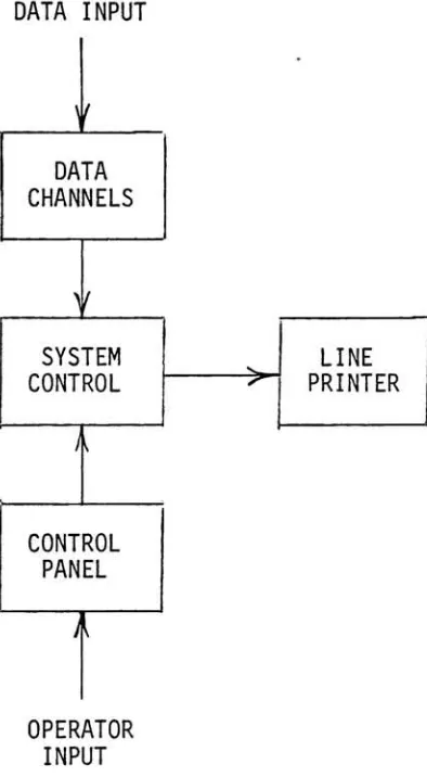
The first level
block diagram
ofthe
S.D.C.S.
is
shownin
Fig.
3.1.
At
this
level,
only the
primary
elements are shown,and
include
the
controlpanel,
data input
conditioners, systemcontrol, and
the
line
printer.The
nextlevel
ofcomplexity
is
shownin Fig.
3.2.
This level
showsthe
system elementsrequired
for interface
to
the
control panel,data
signalconditioning
section, andthe
line
printer.The
requirementfor
systemtiming
and controlis
shownhere,
but
will notbe
developed
untilthe
final
design
approachto
all sub-systemfunctions
is
determined.
The
nextstep
(Fig.
3.3)
in
the
design is
to
define
allthe
functional
elements andtheir
logical
interconnections.
This
design
stageis
still conceptual, without considerations ofimplementation.
Figure
3.3
shows allthe
sub-system componentsof
the S.D.C.S.
The
nexttask
involved
selection ofthe
optimum
digital
oranalog design for
each sub-system.1.
Matthew L.
Fichtenbaum
DATA INPUT
Y
DATA
CHANNELS
^f
SYSTEM
CONTROL
^.LINE
PRINTER
s*1
cCONTROL
PANEL
OPERATOR
INPUT
[image:29.546.220.417.219.577.2]oi LU
X1
CD Q
LU -^
Z 1 LU CL. Q
O o
s:cc
1
LU Z Z i<
WQ.K
< 1 1 1
_lQ Z
fiK V
1 z
o s:cj UJ
ii CC s < => Z O
I Cl. Q Z< U
2*
1 Q
OO z
A
oor
N*
ii1 CC
>
/
HHS! LU>-hh a: o;_i <
s LU 1 a: LU "-^
< o a.
Ts-1 s:Q s a z
<LUZO ^.o
QS<U C CJ
/
S.
A
N
<\
^CC _J -J cc
LUO CDO LU
X cc LU (J z a: X
LUI 1 >-1 Z JS
CJHH 1 eC CD
HH | 2: z
LU 1
V.
O <Q.O O 31 Ll. O HHO CD Q.
CC 1_li CJ
O"
_JCJ Qi _J Io O ii
I lu a. i 1 LU| LU 1|
ZZl/lJQ ZZH(-Q OQ et |
o<ci-hr> z OeC 3 Z Z z 2 3
OD-QS< cj a. OOii ec "<
c s:
1
y,
j
Vj
<
>
r
>
f
_J
eC CD
1
Z
HH i i
co CD et z
O"
Q eC
f-^
oeC CO 1 1
1 1 1>- _l LU
Q
>
_J 1
O =C< car O I eC hh
CC _lCJ Q_l a: _ji cj Zh ^
= Z 0
1 luii a. t LU=") | C =3 1 CD Z
Z Z O O OO ZZO-f* Q. <HO
O et Z Zhh OeC ZT3 CS Z O OOCJ
UQ.h<Q UHmW O HH
_l <C Z 00 o a oo U_ o CD < SC CJ o I ca LU > LU -J I Q O CJ LU oo CM CO LU CC CD
indNi
uoivbBdo
3
CONTROL
PANEL
\1/
CHANNEL
SEL.
SWITCH
DATA TOL.
SWITCH
TOL.
SAMPLE
RATE SWITCH
PRINT RATE
SWITCHES
PRINT REQUEST
PRINT ON/OFF
SWITCHES
DATA DISPLAY
AND
SWITCH
LED
INDICATORS
UP
OPERATOR INPUT
DN
UP
DN
Y~ON
ANALOG
AND
DIGITAL
SUPPORT
MODULES
DIG.
ANAL.
<-/
20
>
OFF
>
CHANNEL
SELECT
CONTROL
DATA TOL.
MEM.
AND
CONTROL
SAMPLE
RATE
CONTROL
RATE
CONTROL
PRINTER
CONTROL
CONTROL
PANEL
INTERFACE
TIME,
DIGITAL,
AND ANALOG
MULTIPLEXER
ANALOG
MULTIPLEXER
vA/D
CONVERTER
INTERFACE
CONTROL
ANALOG
AND
DIGITAL
INPUTS
-2*TIME
> VV ->LINE
PRINTER
SYSTEM
TIMING
AND
CONTROL
t.
SYSTEM
CLOCK
(SECONDS)
DATA
COMPRESSION
CONTROL
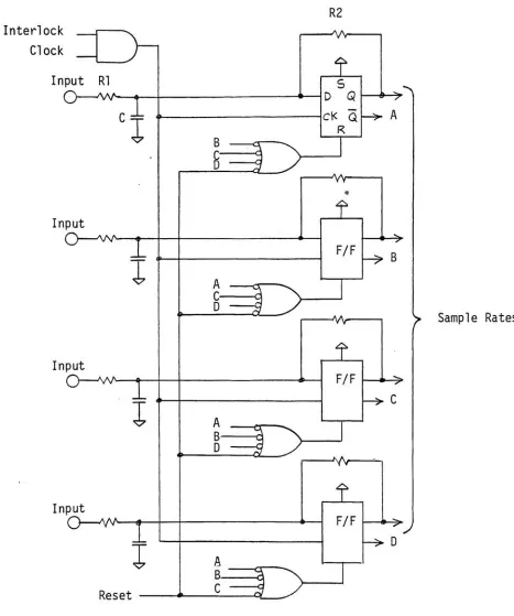
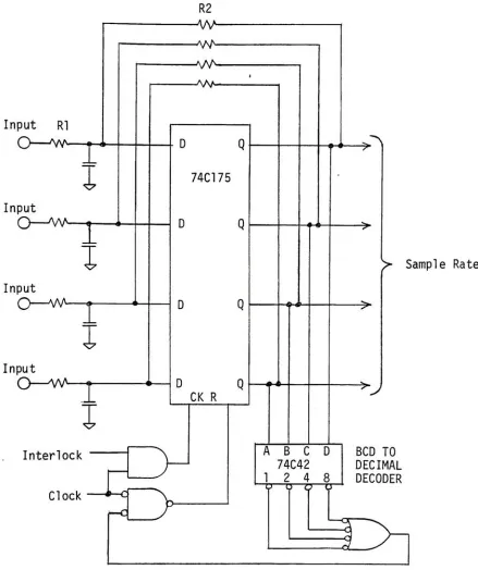
3.2.1
Selection
ofthe
Data Compression Control
Sub-System
This
sub-systemis
selectedfirst
because
it
is
the
most
interdependent
of all sub-systems.The
solutionto this
sub-system will require a specific partialsolution
to
inter-related
sub-systems as willbe
shown.At
this
point, adescription
ofthe
data
compressionfunction is in
order.Data
compressionis
simply
amethod of
reducing
the
amount ofdata
to
be
considered(printed)
for
evaluation.If
a number ofdata
channelsare monitored,
it is
important
to
print alldata
channelsevery time
one or moredata
channels changesby
a"Specific
amount."
This
"specified
amount"can
be defined
asany
ofthe following:
a.
A fixed
amount such as +2C,
+.3VDC, + .27 oz.
-in., etc.
b.
A
percentage ofthe
last
value which caused printout.c.
A
fixed
upper andlower
value.d.
A
limited
number offixed
upper andlower
values.e.
Any
combination of para. a.thru
para. e.The
most acceptable method ofdata
compression wouldbe
one
in
which adata
channel would cause a printout eachtime
it
changedby
a specific amount.This
specificationwould eliminate
the
choices of para. c. andd.
Para.
d.
could
be
used,but
wouldbecome
impractical
if
a greatThe data
compressiontechnique
listed in
para. a.looks
good at
first,
but has
disadvantages because
ofthe
lower
and upper range considerations.
If
anincrement
equalto
one percent of
full
scale(1999)
is
chosen,then
data
at5
percent offull
scale wouldhave
to
changeby
20
percent
to
gofrom 5
to
6
percent offull
scale.Yet,
when
data
changesfrom 50
to 51
percent offull
scale,it has
only increased
by
2
percent offull
scale.Para.
b.
solves
this
problemby
requiring that the
data
changeby
a
fixed
percentage ofthe
last
valueit
had
which causedprintout.
Figure 3.4 illustrates
this.
Note
that
full
scaleis
equalto the
maximum number ofdigital
countsfrom
the
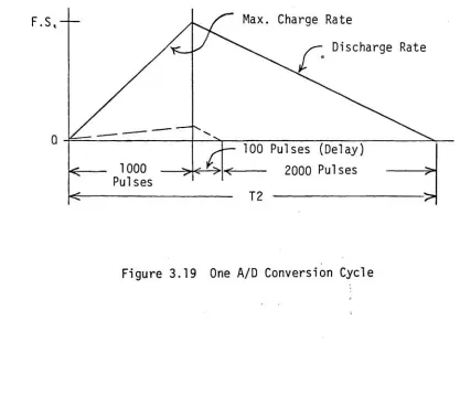
A/D
converter.No
change canbe
less
than
one countfrom
the
A/D
converter.Full
scalehas
been
defined
as a3-1/2
digit
number, or1999
counts.Assume
that
data
channel1
has
atolerance
of10
percent.If
a value of40
counts(point
A)
caused printoutthen
channel
1
cannot cause printout again untilit
changedby
10
percent, orfour
counts.When
channel1
finally
reachesa
10
percentlimit,
printout occurs and a new10
percentwindow
is
created(see
Figure 3.4).
The
methoddescribed
in
para.b.
looks
very good,
but
aproblem can exist on
the
lower
end ofthe
data
range.As
an example, assume
that
a5
percent changeis
selectedfor
channel
1
andit is
presently
at a count(value)
of9.
If
A
LU
<
X
o o
LU
o z
<
cc LU
eC O
-1-ro
cu -. =3 cn
o o
o o
CO
o
r-o CO
o uo
o
-i-o oo
O CM
31V0S llfld
JO lN30U3d
occur each
time
a change of one count occurs.This
canbe
a
very
undesirablefeature.
A
solutionto this
problemcan
be
to
define
the
data
change as a combination ofvariables as
indicated
in
para. e.The
following
combination of variables
may
be
chosento
initiate
printout:
A
percentage(of
the
data
value)
change.t
A
change of atleast
two
countsifrom
the
A/D
conversion),An
absolutedata
value of atleast
15
counts(from
the
A/D
conversion).This
combination of requirementsis
avery
effectivecompromise of all
the
stated options, and willtherefore
be
used.The data
compression system nowhas
adefined
"WINDOW"in
whichdata
may
change withoutcausing
printout.This
"WINDOW"
is
proportionalto
the
data
value(percentage
ofdata),
yethas
a minimum value(+2
counts)
andis
only
active when
the
absolutedata
valueis
greaterthan
aspecified value
(15
counts).As
an example,if
channel10 has
a percentage voltage ofX
and printoutlast
occurred at valueD,
then the
newwindow
is:
D
+(XD
+2)
where
D
>
15
countsA
sub-system solutionto
data
compressiondesign
caninvolve
any
combination ofanalog
anddigital
solutions.An
attempt willbe
madeto
solve eachfunction
using
analog
and/ordigital
solutions.The
requirementfor
the
digital
data
valueto
changeby
at
least
two
countsis
then
an absolutenecessity
because
an
A/D
converteris
required, andA/D
converters alwayshave
a minimum conversionaccuracy
of atleast
+_
.5LSB.
A
typical
A/D
of modest costhas
atotal
accuracy
of + .05percent
(of
full
scale)
+ .5LSB.
For
a3-1/2
digit A/D
converter,
this
translates to
anaccuracy
of +1.5
LSB.
Now that this
part ofthe
data
compression sub-systemis
defined,
we can now consider solutionsfor
the
remainderof
this
sub-system.A
system whichfavors
analog
solutionsis
shownin Figure
3.5.
The
only
function
whichdictates
the
use of adigital
solutionis
the memory for the digital data
anddelta
(/)
data
values.The
closestanalog
solutionto
data
storageis
a sample/holdcircuit.
This is
impossible to
implement because data
may
need
to
be
storedfor
severalhours.
Because the
A/D
converter mustbe
usedfor
the
digital
storage,
the
next questionto
be
askedis
whetherto
selecta
dual
slope or a successive approximationA/D
converter.Present
day
technology
dictates that
adual
slope approachQ.
E eC
CU r XL
s-o> o s-Q.
c
o .
CO cn
CU
s-Q. E o CJ
ra
+->
(C
Q
LO
ro
cu
s-gives
the
mostaccuracy
perdollar
providedthat the
conversion speed requirement can
be
obtained.Another
advantage
to the
dual
slopeA/D
converteris
its
inherent
noise
immunity
due
to the
effectiveintegration
ofthe
data
signal.This
is
a well-knownfeature
and will notbe discussed.
Figure 3.5
showstwo
A/D
converters.One
is
usedto
convertthe
analog
value,
whilethe
secondVd
converteris
usedto
convert a
fractional
value ofthe data
whichis
equalto
the
desired
data
tolerance.
This
methodhas
the disadvantages
of complex
circuitry
andinherent
conversion errors whichexist
in
the
programmable amplifier andthe
additionalA/D
converter.
Figure 3.6
shows abetter
solutionfor obtaining the
data
tolerance
value.This
is
adigital
solution which requiresa
BCD
Rate
Multiplier,
aninput
pulsetrain
from
the
A/D
converter which
is
equalto the
conversion value, and anoutput counter.
The detailed
solutionfor
obtaining the
data
tolerance
value willbe
shownin
section5.3.
The analog
solution(Figure
3.6)
introduces
errorsin
eachD/A
conversion(at
least
+ .05 percentfull
scale,
+ .5LSB),
each amplifier
(+
.1 percentlinearity),
andin
each comparator
(+
.02 percent,long
term).
s-cu
Q.
+J
<U
+J
(O
Q
O CJ CQ
<a
sz (->
c
o
r-CO CO
CU
s-
Q-E
o
CJ
<T5
03 O
CO
CO
CU
Worst
case calculation ofthe
comparetolerance,
E,
is
then:
E
=2
[(.05
+.1 + .02}% + .5
LSB]
=
2
(.17%
+.5
LSB)
=.34 percent
full
scale +1
LSB
This
erroris
tolerable.
The
only shortcoming to this
approach
is
that there
is
no noiseimmunity
for
the
newdata input
to the
comparators, and each comparator wouldrequire an offset
to
widenthe
compare windowby
2
LSB's
as
defined
earlier.The
compareinhibit
signal(Figure 3.6)
is
true
aslong
asnew
data
[VQ
(NEW)]
is
less
than
VR.
The
value ofVR
is
set
to
.75 percent ofthe
full
scaleanalog
voltage.This
circuit satisfies
the
requirementthat
printout shall notbe initiated
whenthe
absolute value ofdata is
equalto
orless
than
15
counts, or .75 percent offull
scale.One
possible modificationto the
sub-systemin Figure 3.6
is
a substitution of oneD/A
converter andthe
analog
ADD/
SUBTRACT
functions
with adigital
solution.Figure 3.7
showsone possible solution.
The
ADD/SUB LOGIC function
eliminatesany
non-linearities which existed whentwo
D/A's
were used,and also eliminated
the
ADD/SUBTRACT
amplifiers andtheir
inherent
errors.At
this
point,
one can seethat the
next possible modification
to the
Data
Compression
Sub-System
wouldinvolve
a100
percentdigital
solution.Figure
3.8
shows a100
LL
O
.Or
to
s-o ->
(O
s-fB Q. E
o CJ
(C
cn O
jQ 00 "O T3 eC
Q "O <u
s-"3
00 cu
cn c
r CO
c o
I to to
cu s-Q.
E
O cj
+J Q
OO cu s_ =3 cn
o oo
(0 Dl
I
to to oi s-Q. E O
CJ
<o M (O O
CO
oo
cu s-3 cn
The ADD/SUBTRACT
andCOMPARE logic
functions
canbe
designed
using
a serial or parallel method.Whichever
method
is
used,both
functions
willbe
accomplishedusing
binary
codeddata because I.C.
manufacturershave favored
a
binary
solutionfor
the
ADD/SUBTRACT function.
The
serial solution
is
attractivebecause less
ICs
arerequired
for
the
ADD/SUBTRACT
and#COMPAREfunctions,
andmuch
less
wiring
is
requiredto
performthe
arithmeticfunctions.
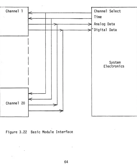
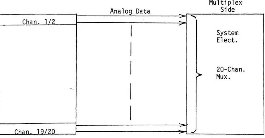
3.2.2
Selection
ofthe
Control
Panel
Interface
Sub-System
a.
Selection
ofControl
Switches
The
control panelis
the
operatorinterface
to the
S.D.C.S.
For
this
reasonits
operation anddata
display
mustbe
easily
understood.Figure 3.3
showsthe
various operatorinput
controls andthe
feedback
control of
the
switchindicators
anddata display.
The
control panellayout is
shownin Figure 3.9.
The
operator canincrement
ordecrement
the
channelnumber and channel
tolerance
tt) the
desired
selection, withthe
data
value ofthe
selected channeldisplayed
with a
3-1/2
digit
pluspolarity
display.
The
switchesand
indicators for
Data
Compression Sample
Rate,
Fixed
Data
Sample
Rate,
Data
Request,
Control
Panel
Lock,
andPrinter
ON/OFF
are onthe
right side ofthe
Control
Panel
.The input
controls canbe
mechanicalswitches,
capacitivetouch
plateswitches,
Hall
effectswitches,
conductivetouch
switches,
etc.Since CMOS logic is
the
primary
I.C.
type
selectedfor
the
S.D.C.S.,
conductivetouch
switches will
be
usedto take
advantage ofthe
high
input impedance
ofCMOS.
b.
Selection
ofthe
Data
Display
Interface
The data
display
interface
is
shownin Figure
3.10
(a).
The
data
display
includes
data
channel number selection(two
digits),
data tolerance
selection(two digits),
and asigned
3-1/2
digit
display
as shown onthe
left
side ofthe
Control
Panel.
A
method mustbe
selectedfor
trans
ferring
this
data
(eight
digits)
from
the
mainlogic
to
the
eightL.E.D.
digits
which arelocated
onthe
control paneldisplay
board.
V au.
O
LULl_ I O CCZ a-o Q- eC S CC O CJ LU _l eC Cl.55
Q 00o
o
o
o
o
CD
Z eC< 1
CD
a: ca:
CD
z
cn
et _!
31O
CJ 1
CD
cn
o
o
CJ
o
o
< O 1 1
eC
LU
o
O
Q
LU
o
O
eC h-\- <C
<C CC Q
LU
o
o
Q J
LU O-X S!
hh eC
o
o
REGISTERS
DIGIT
0
INTERFACE
LED DIGITS
(TYPE
TIL
311)
4
L-/ ^^
DIGIT 1
4
*w
1
/
^'
"
1
DIGIT
7
DECIMAL
POINTS
POLARITY
>
DECIMAL
POINT
^-
TO
"+1"DIGIT
FIGURE
3.10
(a)
MAXIMUM-WIRE
INTERFACE
TO L.E.D.
DISPLAY
A brute-force
methodis
shownin
Figure 3.10(a).
The
(2)
L.E.D.
digits
canbe Texas
Instruments
type
TIL 31
r 'hexidecimal
display
withlogic.
The TIL 311
is
a14-pin
dual-in-line
I.C.
whichpresently
has
a100
piece cost of$6.50
each.The I.C.
containsa
four-bit
latch,
BDC
to
7-segment
decoder,
7
constant-currentdrivers,
andthe
7-segment L.E.D.
display.
The
advantages ofthis
design
are:1)
alow P.C.
board
real-estate requirement,2)
low
assembly
cost,3)
easy to troubleshoot.
The
disadvantages
are:1)
high
cost,2)
37 interface
wires required,3)
high
power
dissipation
of525
milliwatts perI.C.
(nominal),
4)
the
"+ 1"digit is
not availablein
this
series andmust
be separately driven
withdiscrete
components,5)
the
characterheight
of .27inches limits
the
viewing distance
to
10 feet.
This
design
canbe improved
by
replacing
the
TIL
311
display by
the
Type MAN 4610
display^ 'which
is
manufactured
by
Monsanto.
This
L.E.D.
display
has
acharacter
height
of .4inches
and a40
percenthigher
luminous
efficiency than the
TIL 311
for
a segmentcurrent of
five
miHi
amperes.Each L.E.D.
display
requires a
SN74LS47
driver
and seven currentlimiting
resistors.
The
SN74LS47, MAN4610,
and seven resistors costapproximately
$5.00
andhas
atotal
(typical)
(3)
Monsanto,
1977
Solid
State
Optoelectronics,
pp.93-96.
power
dissipation
of210
milliwatts.Disadvantages
of
this
approach are: moreP.C.
board
real estateand
higher
assembly
costthan
the
TIL 311
design.
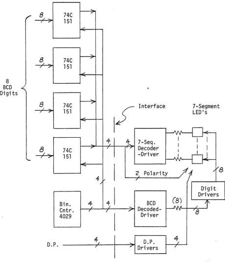
Multiplexing
is
an alternativedesign
approach.With
this
methodonly
oneBCD to
seven segmentdecoder
driver SN7446A
and seven resistors are requiredto
drive
all eightL.E.D.
displays.
The
interface wiring
is
also reducedto
12
signals,
whichinclude four
separate
decimal
point signalsfor
the
3-1/2 digit
data display.
The disadvantage
to this
approachis
the
requirement ofmultiplexing logic
[see
Figure
3.10(b)],and
the
addition ofdigit drivers.
According
to the manufacturers,
whenN
digits
aremultiplexed,
eachdigit
requires .85Ntimes
the
ratedcontinuous current
to
obtainthe
same apparentbrightness.
The
desired L.E.D.
brightness
requires aconstant current of
five
milliamperes per segment.When
multiplexing is
usedfor
eightdigits,
the
required current
(If)
per segmentbecomes:
If
=(.85) (N)
(.005)
=(.85) (8) (.005)
=
.034 amperes
CEq.,
3-1)
8
BCD
J
Digits
74C
151
>
8
74C
151
8
-P>
74C
151
4
4
4
7^D.P.
Interface
7-Segment
LED's
%
7-Seq.
Decoder
-Driver
h-
/W-I
W-2
Polarity
->
BCD
Decoded-Driver
(8)
>
D.P.
Drivers
4
~P
/&
Digit
Drivers
.-f--t
Figure
3.10
(b)
Multiplexed
Interface
to
the
7-Segment
Data Display.
[image:49.546.55.515.66.603.2]The
total
digit
power requirementsis
then:
7
If Vcc
=(7)
(.034) (5)
=1.19
wattsor
149
milliwatts perdigit,
whereVcc
= positivelogic
supply
voltage.The
Texas
Instruments SN7446A
is
aBCD-to-seven-segment decoder/driver
with eachoutput capable of
sinking
40
milliamperes.The Texas
Instruments
SN7445 BCD-to-decimal
decoder/driver
is
required
to
drive
the
digits
viadigit
driver trans
istors.
Both
I.C.'s
require atotal
power of535
milliwatts.
Since
the
National
MM74C151
eight channeldigital
multiplexer andthe RCA CD4029A
presettableup/down counter requires negligible
power,
the total
power
(P.)
perdigit is
then:
P+
=I
-:
Vo
+ .535/8 = .149 + .067t T CC
=
.216 watts per
digit
(Eq.
3-2)
The
multiplex control costsapproximately
$22.00,
or$2.75
perdigit.
Each
digit
costs$2.25,
therefore
the total
costis
$5.00
perdigit.
This
cost andpower
dissipation is
equalto the
previousdesign
approach,
but
requiresless P.C.
board
real estateand much
less
interface
wiring.This design
approachwill
then
be
used.The detailed design
ofthis
function
canbe
accomplished at
this
time
because its
operationis
notsystem-dependent.
Figure 3.11
showsthis
sub-systemdesign.
Note
that the transistors
and resistors arein I.C.
form,
andthat
nodiscrete
components aremounted
directly
onthe
P.C.
board.
This
requirementmakes
it
very
convenientto
replacedefective
components
because
all components are mountedin I.C.
sockets.
OOOO
;aj <jQ
jj j-j UlInlu Ul
<