This is a repository copy of
Analytical formulation for the shielding effectiveness of
enclosures with apertures
.
White Rose Research Online URL for this paper:
http://eprints.whiterose.ac.uk/90051/
Version: Accepted Version
Article:
Robinson, M P orcid.org/0000-0003-1767-5541, Benson, T M, Christopoulos, C et al. (5
more authors) (1998) Analytical formulation for the shielding effectiveness of enclosures
with apertures. IEEE Transactions on Electromagnetic Compatibility. pp. 240-248. ISSN
0018-9375
https://doi.org/10.1109/15.709422
[email protected] https://eprints.whiterose.ac.uk/
Reuse
Items deposited in White Rose Research Online are protected by copyright, with all rights reserved unless indicated otherwise. They may be downloaded and/or printed for private study, or other acts as permitted by national copyright laws. The publisher or other rights holders may allow further reproduction and re-use of the full text version. This is indicated by the licence information on the White Rose Research Online record for the item.
Takedown
If you consider content in White Rose Research Online to be in breach of UK law, please notify us by
Analytical Formulation for the Shielding
Effectiveness of Enclosures with Apertures
Martin Paul Robinson, Trevor M. Benson, Christos Christopoulos,
Member, IEEE, John F. Dawson,
M. D. Ganley, A. C. Marvin, S. J. Porter, and David W. P. Thomas,
Member, IEEEAbstract—An analytical formulation has been developed for the
shielding effectiveness of a rectangular enclosure with an aper-ture. Both the magnetic and electric shielding may be calculated as a function of frequency, enclosure dimensions, aperture di-mensions and position within the enclosure. Theoretical values of shielding effectiveness are in good agreement with measurements. The theory has been extended to account for circular apertures, multiple apertures, and the effect of the enclosure contents.
Index Terms— Apertures, circuit modeling, electromagnetic
compatibility, electrical equipment enclosures, electromagnetic shielding.
I. INTRODUCTION
E
LECTROMAGNETIC shielding is frequently used to re-duce the emissions or improve the immunity of electronic equipment. The ability of a shielding enclosure to do this is characterized by its shielding effectiveness, defined as the ratio of field strengths in the presence and absence of the enclosure. At each point in an enclosure, we can define an electric shielding effectiveness and a magnetic shielding effectiveness .For an infinite conducting sheet illuminated by a plane wave, and are equal and depend only on the frequency and on the conductivity, permeability, and thickness of the sheet. However, if an enclosure is made from the sheet, then and are generally different and become dependent on the position within the enclosure. Furthermore, it is practically found that the shielding is determined mainly by penetration of energy through apertures in the enclosure rather than through the walls, although an exception to this finding can be at audio frequencies. In this paper, we assume that the conductivity of the enclosure walls is sufficiently high that only aperture penetration is important.
Shielding effectiveness can be calculated by numerical sim-ulation or by analytical formsim-ulations. Numerical methods can model complex structures but often require much computing time and memory in order to model a problem with sufficient
Manuscript received March 26, 1997; revised May 27, 1998. This work was supported by the Engineering and Physical Sciences Research Council under Grants GR/J09086 and GR/J10396.
M. P. Robinson, J. F. Dawson, M. D. Ganley, A. C. Marvin, and S. J. Porter are with the Department of Electronics, University of York, Heslington, York, Y010 5DD U.K.
T. M. Benson, C. Christopoulos, and D. W. P. Thomas are with Department of Electrical and Electronic Engineering, University of Nottingham, Notting-ham, NG7 2RD U.K.
Publisher Item Identifier S 0018-9375(98)06191-2.
detail. This means that although they are good at predicting the shielding of a particular enclosure, it is difficult for designers to use them to investigate the effect of design parameters on and . Numerical methods that have been used to calculate shielding include transmission-line modeling [1], finite-difference time-domain (FDTD) method [2], and method of moments (MoM) [3].
Analytical formulations provide a much faster means of cal-culating shielding effectiveness, enabling the effect of design parameters to be investigated (we use the term formulation rather than solution, as they often use empirical relationships rather than fundamental principles). Many of these are derived from Bethe’s theory of diffraction through holes [4] and apply only to electrically small apertures. Other formulations include that of Hill et al. [5], derived from a power-balance method and the widely quoted formula of Ott [6], where is wavelength and is aperture length.
Our aim here has been to derive a relatively simple for-mulation that incorporates all the relevant design parameters without placing inconvenient restrictions on their range. We follow Mendez [7] in considering the enclosure as a wave-guide, and assume a single mode of propagation (the mode). However, our formulation applies above the cutoff frequency for this mode as well as below. Both electric and magnetic shielding are calculated as functions of frequency, aperture dimensions, enclosure dimensions, wall thickness, and position within the enclosure. Simple modifications enable multiple apertures and internal losses to be included. At present, our formulation applies only to rectangular enclosures, but these comprise a large proportion of shields used in practical electronic design. It may be applied to electrically large and small apertures.
II. THEORY
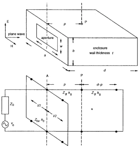
A rectangular aperture in an empty rectangular enclosure is represented by the equivalent circuit of Robinson et al. [8], which is shown in Fig. 1. The longer side of the slot is shown normal to the -field, which is the worst case for shielding. The electric shielding at a distance from the slot is obtained from the voltage at point in the equivalent circuit, while the current at gives the magnetic shielding. The radiating source is represented by voltage and impedance and the enclosure by the shorted waveguide whose characteristic impedance and propagation constant are and . We
©1998 IEEE. Personal use of this material is permitted. Permission from IEEE must be obtained for all other uses, in any current or future media, including reprinting/republishing this material for advertising or promotional purposes, creating new collective works, for resale or redistribution to servers or lists, or reuse of any copyrighted component of this work in other works.
Fig. 1. Rectangular box with aperture and its equivalent circuit.
proceed by first finding an equivalent impedance for the slot and then using simple transmission line theory to transform all the voltages and impedances to point .
A. Slot Impedance
The aperture is represented as a length of coplanar strip transmission line, shorted at each end (implying that we need only consider the transmission line currents on the front face of the enclosure). The total width is equal to the height of the enclosure and the separation is equal to the width of the slot . Its characteristic impedance is given by Gupta et al. [9] as , where and are elliptic integrals. The effective width is given by
(1)
where is the thickness of the enclosure wall. If
(which is true for most practical apertures) then, according to Gupta et al., the following approximation may be used:
[image:3.612.319.540.69.228.2](2)
Fig. 2 shows this variation of with .
To calculate the aperture impedance , we transform the short circuits at the ends of the aperture through a distance to the center. This is represented by point in the equivalent circuit. It is necessary here to include a factor to account for the coupling between the aperture and the enclosure
(3)
[image:3.612.363.556.413.477.2]This accounts for the connection between transmission line and waveguide.
Fig. 2. Characteristic impedanceZ0sof aperture as a function ofwe=b.
B. Electric and Magnetic Shielding Effectiveness
By Th`evenin’s theorem, combining , , and gives
an equivalent voltage and source
impedance . For the mode
of propagation, the waveguide has characteristic impedance and propagation constant , where . Note that and are imaginary at frequencies below the cutoff (equal to ). We now transform , , and the short circuit at the end of the waveguide to , giving an equivalent voltage , source impedance , and load impedance
(4)
(5)
(6)
The voltage at is now , and the current
at is .
In the absence of the enclosure, the load impedance at is simply . The voltage at is and the current is , The electric and magnetic shielding are, therefore, given by
(7)
(8)
C. Extensions to the Formula
We have extended the theory to account for electromagnetic losses, circular apertures, and multiple apertures.
TABLE I
ENCLOSURES USED FORSHIELDINGMEASUREMENTS
characteristic impedance and propagation constant
(9)
(10)
These can be substituted for and in the calculations in Section II-B.
Turner et al. [12] have found that the shielding effectiveness of a round hole is approximately the same as that of that of a square aperture of the same area. The formulation can, therefore, be applied to circular apertures by letting
(11)
where is the diameter of the aperture.
If there are similar apertures in one face of the enclosure, then the individual aperture impedances must be combined. We have assumed that the individual impedances may simply be combined in series, giving a total impedance
(12)
The calculations then proceed as in Section II-B. This simple approach ignores the mutual admittance between apertures and may not be applicable if the apertures are too close together.
III. MEASUREMENTS
The shielding effectiveness of a range of enclosures and apertures was measured. Apertures were either cut into the walls of the enclosures or into removable plates. These were attached with finger stock to ensure good contact at the joints. The lids of the enclosures were fastened with gaskets, finger stock, or closely spaced screws for the same reason. Table I lists the relevant parameters of the enclosures. The aperture length ranged from 40 to 200 mm and the width from 4 to 80 mm.
[image:4.612.315.544.64.214.2]Shielding measurements were made by placing sensors in the enclosure, or by observing the emissions from a radiating circuit within the enclosure. Measurements with sensors were made in screened rooms. The source of the field was a network analyzer connected via an amplifier to a stripline [13], log periodic, or Bilog [14] antenna. The rooms were dampened with absorbing material to reduce the effects of resonances. To measure , a monopole antenna in the lid of the enclosure sensed the field. It was coupled via a cable or an optical link to the second port of the network analyzer. Fig. 3 shows the
Fig. 3. Method of measuring electric shieldingSE.
[image:4.612.76.263.86.157.2]Fig. 4. Method of measuring magnetic shieldingSM.
Fig. 5. Digital circuit used for measurement of shielding. Oscillator fre-quency 10 MHz.
[image:4.612.321.545.259.381.2]Fig. 6. CalculatedSEat three positions in 3002 120 2 300 mm enclosure with 1002 5 mm aperture.
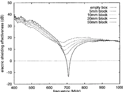
The monopole sensor was also used to measure of the 300 120 300 mm enclosure containing lossy elements. To introduce electromagnetic losses, various unpowered circuit boards were placed in the enclosure. Blocks of radio absorbing material (RAM) were also used. These were placed on the floor of the enclosure, and offset from the center to prevent them touching the sensor. The blocks were 130 mm wide (i.e., parallel to the slot), 60 mm high (i.e., perpendicular to the slot), and 5–50 mm thick (i.e., along the direction of propagation). The effect of block thickness on the shielding was investigated.
IV. RESULTS
A. Electric Shielding Effectiveness
[image:5.612.64.272.67.226.2]Fig. 6 shows the calculated at three positions within the unloaded 300 300 120 mm enclosure with a 100 5 mm aperture. The calculations show that the enclosure resonates at approximately 700 MHz, leading to negative shielding (field enhancement) around this frequency. Below the resonant frequency, decreases with frequency and increases with distance from the aperture.
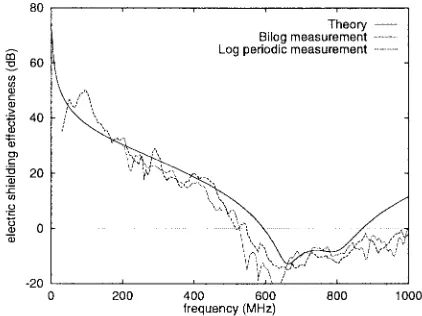
Fig. 7 shows the calculated and measured at the center of the box ( mm). We can see that there is good agree-ment, both above and below the cutoff frequency of 500 MHz. Note that much of the variation in the measurements is due to the imperfect damping of resonances in the screened room. These shift in frequency when the enclosure is placed in the room, leading to the “noisy” appearance of the plots of shield-ing versus frequency. The agreement at the two other positions ( mm and mm) was also good. Fig. 8 shows the calculated and measured for a larger aperture, size 200 30 mm. The resonance is broader and the low-frequency shielding is worse at than that of the smaller aperture.
[image:5.612.325.536.278.436.2]Fig. 9 shows the calculated and measured at the center of the 222 55 146 mm box while Fig. 10 shows these quantities at the center of the 483 120 483 mm box. In each case the aperture was 100 5 mm. It can be seen from these figures that the smaller box does not resonate below 1 GHz, while the larger box shows resonances at 440 and 980 MHz.
Fig. 7. Calculated and measured SE at center of 3002 120 2 300 mm enclosure with 1002 5 mm aperture.
Fig. 8. Calculated and measured SE at center of 3002 120 2 300 mm enclosure with 2002 30 mm aperture.
Fig. 9. Calculated and measured SE at center of 2222 55 2 146 mm enclosure with 1002 5 mm aperture.
B. Magnetic Shielding Effectiveness
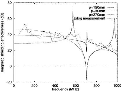
Fig. 11 shows of the 300 300 120 mm enclosure with a 100 5 mm aperture, calculated at
[image:5.612.326.538.492.652.2]Fig. 10. Calculated and measuredSE at center of 4832 120 2 483 mm enclosure with 1002 5 mm aperture.
Fig. 11. CalculatedSMat three positions in 3002 120 2 300 mm enclosure with 1002 5 mm aperture, and measured SM at center of enclosure.
resonance at 700 MHz can be seen at mm and mm, but is less pronounced at the center of the box ( mm). This is expected from the mode structure of the resonance. At low frequencies, increases with distance from the aperture (as does ), but is almost independent of frequency.
Fig. 11 also shows that there is good agreement between calculated and measured at the center of the box ( mm). Agreement was also good at mm, where the resonance at 700 MHz was seen in the measurements. Agreement was slightly worse just behind the slot ( mm), with the calculated values of being 5–10 dB higher than the measurements at low frequencies.
C. Change in Emissions
Fig. 12 shows the shielding of the 300 120 300 mm enclosure with a 150 40 mm aperture obtained from the difference in emissions between the shielded and unshielded circuit. The enclosure resonance can be seen, although its frequency is some 50 MHz lower, presumably because of the loading effect of the circuit on the enclosure. The
cal-culated values of and are also shown in Fig. 12. At low frequencies, the reduction in emissions lies between the calculated and . This might be expected as a typical circuit board is a source of both electric and magnetic fields.
D. Effect of Electromagnetic Losses
Introducing the loss term into the formulation does not greatly affect the calculated shielding effectiveness, except around the resonant frequencies. Fig. 13 shows at the center of the 300 300 120 mm enclosure with a 100 5 mm aperture for various values of . We can see that increasing the loss damps the resonance, improving the shielding. It also lowers the resonant frequency.
[image:6.612.65.272.64.223.2]Fig. 14 shows of this enclosure and aperture with various sized blocks of RAM inside. We see that as the thickness increases, the resonant frequency shifts in the manner predicted by the theory and shown in Fig. 13. Placing single-sided circuit boards in the enclosure had a similar effect on the shielding. Fig. 15 shows this for two boards, one (PCB 1) loaded mainly with integrated circuits, resistors and capacitors, the other (PCB 2) a power supply board carrying a mains
Fig. 13. Effect of loss term ζ on calculated SE.
[image:6.612.322.533.276.436.2] [image:6.612.64.273.284.442.2]transformer. Note how PCB 2 introduces a second resonance at approximately 860 MHz.
E. Circular Apertures
We measured at the center of the 300 300 120 mm enclosure with a square aperture of side 77 mm and a circular aperture diameter 88 mm. Each aperture’s area was approximately 6000 mm . The values of for these apertures did not differ by more than 2 dB over the frequency range of 200–1000 MHz.
Fig. 16 shows the measured and calculated at the center of the enclosure with the circular aperture. Also shown are the values calculated from Ott [6] and from Hill et al. [5]. Although these show the right frequency dependence at low frequencies, they do not predict the resonance at 700 MHz. The new formulation gives better agreement both at low frequencies and at the resonance.
We also compared our formulation with measurements described in the literature. Steenbakkers et al. [15] measured the magnetic shielding effectiveness at various positions in a 150 150 150 mm enclosure with a round aperture in one wall. Our analytical formulation gives values of
TABLE II
REDUCTION INSE DUE TONUMBER OFAPERTURES
within 10 dB of their results. Steenbakkers et al. found that increasing the hole diameter from 30 to 60 mm reduced by 12 dB. The analytical formulation predicts a reduction of 14 dB. The measurements of Steenbakkers et al. also show that at subresonant frequencies, increases with distance from the aperture—an effect predicted by our formulation and seen in Fig. 11.
F. Multiple Apertures
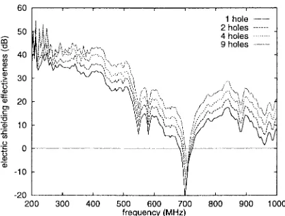
We measured at the center of the 300 300 120 mm enclosure with one, two and three 160 4 mm apertures. For these measurements, the box with a single aperture was used as the calibration standard. This greatly reduced the artifacts due to the resonances of the room, because merely changing the number of apertures did not significantly alter the frequencies of these resonances. Increasing the number of apertures was found to reduce the shielding effectiveness. Table II shows the calculated reduction in at 400 MHz compared to measurements over the range 200–600 MHz.
The analytical solution predicts that and are in-creased by increasing the number of apertures while keeping the total area the same. Fig. 17 shows the measured at the center of the 300 300 120 mm enclosure with one, two, four, and nine apertures. In each case the total area was 6000 mm . As predicted, having more but smaller holes improves the shielding.
[image:7.612.325.536.59.219.2]We investigated the effect of dividing a 100 5 mm slot into several shorter slots using the same enclosure as above. Table III shows the calculated and measured increase in and . The measured increase is slightly more than predicted.
Fig. 15. Measured SEwith two different circuit boards in enclosure.
[image:7.612.64.272.65.221.2]
Fig. 16. Measured and calculated SEat center of 300x120x300 mm
[image:7.612.64.272.286.444.2]TABLE III
IINCREASE INSE ANDSMDUE TODIVIDINGSLOT
Fig. 18 shows at the center of the same enclosure with two designs of ventilation plate, one with three 160 4 mm slots, the other with 20 12-mm-diameter holes. Although the total area of metal removed is about the same, is up to 30 dB greater for the circular holes than for the slots. The “jagged” appearance of the measured results is due to resonances in the screened room. The agreement between theory and measurements is surprisingly good, considering the simple treatment of multiple apertures in (12).
V. DISCUSSION
The analytical formulation presented here provides a fast means of investigating the effect of design parameters on the shielding effectiveness of an enclosure. It confirms that long thin apertures are worse than round or square apertures of the same area. For a typical sized enclosure, the theory predicts that doubling the length of a slot reduces and by about 12 dB, while doubling the width only reduces and by about 2 dB. Calculations using the new formulation show that doubling the number of apertures reduces both and by about 6 dB. However, dividing a long slot into two shorter ones increases and by about 6 dB.
The theory predicts that the size of the enclosure is also im-portant to shielding performance. At subresonant frequencies, doubling the enclosure dimensions while keeping the aperture constant is predicted to increase by about 6 dB and by about 13 dB. However, doubling the dimensions of both enclosure and aperture is predicted to reduce by about 6 dB and by about 1 dB. Furthermore, doubling the enclosure
size halves the lowest resonant frequency. A small enclosure is, therefore, generally preferable to a large one.
There are two points to make concerning the contents of the enclosure. First, and are lower nearer the aperture, so noisy or sensitive circuits should be placed as far from the aperture as possible. Secondly, the contents damp the enclosure resonances, mitigating the negative shielding seen at the resonant frequencies of an unloaded (i.e., empty) enclosure. Our calculation has assumed that the conductivity of the walls of the enclosure is so high that the only significant path of energy is through the aperture. This may not always be so, particularly for low frequency magnetic fields. Field [16], following Kaden [17], gives equations for the electric and magnetic shielding of conducting spherical shells. These indicate that of an unbroken shell is always high unless the walls are very thin or are poor conductors. However is zero for static magnetic fields if the shell is made from nonmagnetic material. The magnetic shielding rises with frequency, first because of field cancellation by eddy currents, and then also because of the skin effect. For the enclosures and apertures investigated in this study, the frequency at which the “finite conductivity” becomes comparable to the “aperture” is at 10–100 kHz. Our assumption of aperture dominance is therefore valid over our measurement frequency range of 1–1000 MHz. The results of Steenbakkers et al. [15] suggest that there is a smooth transition between the two effects. If the enclosure was made from a coated plastic or a conductive polymer the transition would be at a higher frequency.
The analytical formulation assumes a single, mode of propagation. Higher order modes would be able to propagate at frequencies greater than . For all but the largest enclosure studied, the and higher modes could not propagate below 1000 MHz. For the 483 120 483 mm enclosure, the cutoff frequencies of the and modes are 621 and 931 MHz, respectively. However, Fig. 10 shows that the theory gives good agreement with measurement up to 1000 MHz. This may be because the coupling to the higher order modes is not significant for the enclosures and apertures studied. Multimode propagation in a shielded enclosure has been successfully modeled [18], but considerable work would
Fig. 18. Calculated and measured SE for ventilation plates with either three 160mm long slots or twenty 12mm diameter holes (centre of 300x120x300mm enclosure).
[image:8.612.65.273.65.223.2][image:8.612.327.540.66.226.2]
be needed to incorporate such calculations into the formulation discussed here.
In this study, we have placed the aperture centrally in one face of the enclosure, and considered the electromagnetic fields along the midline. For an off-center aperture (e.g., a gap underneath a lid), there might be transverse as well as longitudinal propagation. Further work is needed in this area. An advantage of the formulation is that it accounts for the thickness of the enclosure walls. This is often difficult in numerical methods, which assume infinitesimally thin walls. The formulation might however be inaccurate if the width of the aperture were small compared to the wall thickness . The aperture would itself then act as a waveguide operating below its cutoff frequency, leading to attenuation within the aperture and giving greater shielding than predicted.
VI. CONCLUSION
The formulation described above gives good agreement with measurements over a wide frequency range. It can predict the electric and magnetic shielding effectiveness of a rectangular enclosure with one or more apertures in one wall, both at low frequencies and at resonance. It can be applied to round, square, and rectangular apertures and the size of the aperture need not be small compared to the enclosure. A loss factor has been introduced to describe the damping of resonances by the contents of the enclosure, although further work is needed to characterize this factor for typical electronic equipment. The calculation of electric and magnetic shielding depends upon the frequency and polarization of the applied field, the dimensions of the enclosure and the aperture(s), the number of apertures, and the position within the enclosure. The formulation will, therefore, be of use to designers of shielded enclosures.
REFERENCES
[1] C. H. Kraft, “Modeling leakage through finite apertures with TLM,” in IEEE Int. Symp. Electromagn. Compat., Chicago, IL, Aug. 1994, pp. 73–76.
[2] K. S. Kunz and R. J. Luebbers, The Finite Difference Time Domain
Method for Electromagnetics. Orlando, FL: CRC, 1993.
[3] G. Cerri, R. De Leo, and V. M. Primiani, “Theoretical and experimental evaluation of the electromagnetic radiation from apertures in shielded enclosures,” IEEE Trans. Electromagn. Compat., vol. 34, pp. 423–432, Nov. 1992.
[4] H. A. Bethe, “Theory of diffraction by small holes,” Phys. Rev. 2nd
Ser., vol. 66, pp. 163–182, 1944.
[5] D. A. Hill, M. T. Ma, A. R. Ondrejka, B. F. Riddle, and M. L. Crawford, “Aperture excitation of electrically large, lossy cavities,” IEEE Trans.
Electromagn. Compat., vol. 36, pp. 169–178, Aug. 1994.
[6] Henry W. Ott, Noise Reduction Techniques in Electronic Systems, 2nd ed. New York: Wiley, 1988 (ISBN 0-471-85068).
[7] H. A. Mendez, “Shielding theory of enclosures with apertures,” IEEE
Trans. Electromagn. Compat., vol. 20, pp. 296–305, May 1978.
[8] M. P. Robinson, J. D. Turner, D. W. P. Thomas, J. F. Dawson, M. D. Ganley, A. C. Marvin, S. J. Porter, T. M. Benson, and C. Christopoulos, “Shielding effectiveness of a rectangular enclosure with a rectangular aperture,” Electron. Lett., vol. 32, no. 17, pp. 1559–1560, 1996. [9] K. C. Gupta, R. Garg, and I. J. Bahl, Microstrip Lines and Slotlines.
Norwood, MA: Artech House, 1979, ch. 7.
[10] J. F. Dawson, J. Ahmadi, and A. C. Marvin, “Reduction of radiated emissions from apertures in resonant enclosures by the use of absorptive materials,” in 8th Int. Conf. Electromagn. Compat., Edinburgh, U.K., Sept. 1992, pp. 207–212.
[11] I. D. Woods, “Admittance transformation using precision air-dielectric coaxial lines and connectors,” Proc. Inst. Elect. Eng., vol. 118, pp. 1667–1674, 1971.
[12] J. D. Turner, T. M. Benson, C. Christopoulos, D. W. P. Thomas, M. P. Robinson, J. F. Dawson, M. D. Ganley, A. C. Marvin, and S. J. Porter, “Characterization of the shielding effectiveness of equipment cabinets containing apertures,” in Int. Symp. EMC, Rome, Italy, Sept. 1996, pp. 574–578.
[13] Int. Electrotech. Commission, Int. Standard IEC 801 Part 3: “Method of evaluating susceptibility to radiated electromagnetic energy,” 1984. [14] S. J. Porter and A. C. Marvin, “A new broadband EMC antenna for
emissions and immunity,” in Int. Symp. EMC, Rome, Italy, Sept. 1994, pp. 75–79.
[15] L. W. Steenbakkers, M. P. de Goeje, and J. Catrysse, “The influence of slots and holes on the shielding efficiency of a housing,” in 10th Int.
Symp. EMC, Zurich, Switzerland, Mar. 1993, pp. 469–474.
[16] J. C. G. Field, “An introduction to electromagnetic screening theory,” in
Inst. Elect. Eng. Colloq. Screening Shielding, London, U.K., Nov. 1983,
pp. 1/1–1/15.
[17] H. Kaden, Wirbelstr¨ome und Schirmung in der Nachrichtentechnik. Berlin, Germany: Springer-Verlag, 1959.
[18] M. C. Render and A. C. Marvin, “A multiple mode equivalent trans-mission line model of crosstalk between conductors in shielded envi-ronments,” IEEE Trans. Electromagn. Compat., vol. 37, pp. 488–494, Aug. 1995.
Martin Paul Robinson was born in Oxford, U.K., in 1963. He received the B.A. and M.A. degrees from the University of Cambridge, U.K., in 1986 and 1990, the M.Sc. degree in medical physics from the University of Aberdeen, U.K., in 1990, and the Ph.D. degree in dielectric imaging from the University of Bristol, U.K., in 1994.
From 1986 to 1988, he worked for at the National Physical Laboratory, U.K., and from 1990 to 1993 at the Bristol Oncology Centre, U.K. Since 1993 he has been a Research Fellow at the University of York, U.K. His research interests include design for electromagnetic compatibility, dielectric measurements, and the interaction of electromagnetic radiation with biological tissues.
Trevor M. Benson was born in Sheffield, U.K., in 1958. He received the first class honors degree in physics and the Ph.D. degree in electronic and elec-trical engineering from the University of Sheffield, U.K., in 1979 and 1982, respectively.
After spending over six years (1986–1989) as a Lecturer at University College Cardiff, U.K., he joined the University of Nottingham, U.K., as a Se-nior Lecturer in electrical and electronic engineering in 1989. He was promoted to the Reader of Photon-ics in 1994 and Professor of optoelectronPhoton-ics in 1996. His present research interests include experimental and numerical studies of electromagnetic fields and waves, with particular emphasis on propagation in optical waveguides, silicon based photonic circuits and electromagnetic compatibility.
Dr. Benson received the Clark Prize in Experimental Physics from The University of Sheffield in 1979.
Christos Christopoulos (M’92) was born in Patras, Greece, on September 17, 1946. He received the Diploma degree (electrical and mechanical bngineering) from the National Technical University of Athens, Athens, Greece, in 1969, and the M.Sc. and D.Phil. degrees from the University of Sussex, U.K., in 1970 and 1974, respectively.
John F. Dawson is a member of the Applied Electromagnetics Research Group, University of York, U.K. His research interests include transmission-line matrix (TLM) modeling, electromagnetic compatibility prediction for circuits and systems, and electromagnetic compatibility test environments.
M. D. Ganley, photograph and biography not available at the time of publication.
A. C. Marvin has five years research experience as a graduate student and Research Fellow in the Department of Electrical and Electronic Engineering, University of Sheffield, U.K., on the development of active superdirective array antennas. He spent two years with the Electromagnetic Compatibility (EMC) Group at B.Ae Filton working on EMC ATE system calibration. He was an Aappointed Lecturer in the Department of Electronics, University of York, U.K., in 1979, a Senior Lecturer in 1986, and a Professor in 1995 at the same university. He worked in the Concordia University EMC Laboratory, Montreal, Canada, for a five month period in 1985, using numerical techniques to solve radiated emission problems. He is the joint inventor of the BILOG series of EMC measurement antennas produced by Chase EMC which is sold worldwide. His research activities have included improvements to EMC emission measurement techniques in screened enclosures and open area test sites, the structure of fields close to radiating sources, and the development of CAD tools for EMC design. More recently, he has been involved with the reduction of radiated emissions from equipment enclosures by spurious energy absorption and the development of calibration procedures for screened room-antenna combinations for radiated emission measurements. This latter work is directed toward a revision of Def Std 59/41 now in the final stages of preparation. He was the Applied Electromagnetics Research Group Leader, the Master of Science EMC Course Director, the Technical Director of York EMC Services Ltd., York, U.K.
Dr. Marvin was an Associate Editor for IEEE TRANSACTIONS ON
ELECTROMAGNETIC COMPATIBILITY, Chairman of IEE Professional Group S4 (Fundamental aspects of measurements) for the 1997/1998 session, Vice Chairman of the COST 243 (EMC) Management Committee, and the External Ph.D examiner at the Universities of Liverpool, Sheffield, Nottingham, Surrey, Dublin, Leeds, East Anglia, and Preston Polytechnic (CNAA).
S. J. Porter, photograph and biography not available at the time of publication.
David W. P. Thomas (M’95) was born in Padstow, U.K., on May 5, 1959. He received the B.Sc. degree in physics from Imperial College of Science and Technology, London, U.K., the M.Phil. degree in Space Physics from Sheffield University, U.K., and the Ph.D. degree in electrical engineering from Nottingham University, U.K., in 1981, 1987, and 1990, respectively.
In 1990, he joined the Department of Electrical and Electronic Engineering at the University of Nottingham, U.K., as a Lecturer. His research interests are in electromagnetic compatibility, electrostatic precipitation, and the protection and simulation of power networks.