Processors for Energy Efficient High
Performance Computing: The Texas
Instruments Keystone II
Gaurav Mitra
A thesis submitted for the degree of
Doctor of Philosophy (Computer Science)
The Australian National University
First, I would like to thank my supervisor, Prof. Alistair Rendell for his in-valuable guidance and encouragement throughout my time at the ANU. This thesis would not have been possible without Alistair’s continued support and unwavering patience.
I would like to thank Dr. Eric McCreath, Dr. Josh Milthorpe, Dr. Ashvin Parameswaran and Dr. Joseph Antony for reviewing parts of my thesis and pro-viding useful feedback. My colleagues, Anish Varghese and Arindam Sharma also reviewed portions of my thesis, for which they have my gratitude.
The Australian National University and the Australian Government have supported me financially with an undergraduate scholarship, an Australian Postgraduate Award and numerous teaching opportunities throughout the du-ration of my studies in Australia. I am deeply grateful. I would also like to thank CSIRO for the financial support I received from the ICT Centre Postgrad-uate Research Scholarship during the first six months of my PhD. In addition, I would like to acknowledge financial support from the Australian Research Council Discovery Project (DP0987773).
Major elements of this work were made possible with support from Texas Instruments Inc. In particular, I would like to thank my managers at TI, Ajay Jayaraj and Dr. Eric Stotzer for their guidance throughout my internship at TI. My work with nCore HPC enabled significant parts of this work. I would like to thank Ian Lintault for providing me with the opportunity to work on the nCore BrownDwarf system.
My time at the ANU has been very enjoyable and in particular with the Computer Systems Group and the Research School of Computer Science. I have had spirited discussions with many colleagues at the university which have led to new and interesting ideas. I would like to thank all my friends and colleagues at the ANU for enriching my time here.
For final months of my PhD, I was employed full-time at the National Com-putational Infrastructure where I found immense encouragement. In particular, I would like to thank Dr. Roger Edberg and Dr. Muhammad Atif.
Finally, I would like to thank my mother, Dr. Rupa Mitra; my father, Dr. De-basis Mitra; and my wife Arya Bhattacharjee for their endless love, inspiration, and optimism. This journey would not have been possible without them.
The High Performance Computing (HPC) community recognizes energy con-sumption as a major problem. Extensive research is underway to identify means to increase energy efficiency of HPC systems including consideration of alterna-tive building blocks for future systems. This thesis considers one such system, the Texas Instruments Keystone II, a heterogeneous Low-Power System-on-Chip (LPSoC) processor that combines a quad core ARM CPU with an octa-core Dig-ital Signal Processor (DSP). It was first released in 2012.
Four issues are considered: i) maximizing the Keystone II ARM CPU perfor-mance; ii) implementation and extension of the OpenMP programming model for the Keystone II; iii) simultaneous use of ARM and DSP cores across multiple Keystone SoCs; and iv) an energy model for applications running on LPSoCs like the Keystone II and heterogeneous systems in general.
Maximizing the performance of the ARM CPU on the Keystone II system is fundamental to adoption of this system by the HPC community and, of the ARM architecture more broadly. Key to achieving good performance is exploitation of the ARM vector instructions. This thesis presents the first detailed comparison of the use of ARM compiler intrinsic functions with automatic compiler vector-ization across four generations of ARM processors. Comparisons are also made with x86 based platforms and the use of equivalent Intel vector instructions.
Implementation of the OpenMP programming model on the Keystone II sys-tem presents both challenges and opportunities. Challenges in that the OpenMP model was originally developed for a homogeneous programming environment with a common instruction set architecture, and in 2012 work had only just begun to consider how OpenMP might work with accelerators. Opportunities in that shared memory is accessible to all processing elements on the LPSoC, offering performance advantages over what typically exists with attached ac-celerators. This thesis presents an analysis of a prototype version of OpenMP implemented as a bare-metal runtime on the DSP of a Keystone I system. An implementation for the Keystone II that maps OpenMP 4.0 accelerator directives to OpenCL runtime library operations is presented and evaluated. Exploitation of some of the underlying hardware features of the Keystone II is also discussed. Simultaneous use of the ARM and DSP cores across multiple Keystone II boards is fundamental to the creation of commercially viable HPC offerings based on Keystone technology. The nCore BrownDwarf and HPE Moonshot
systems represent two such systems. This thesis presents a proof-of-concept implementation of matrix multiplication (GEMM) for the BrownDwarf system. The BrownDwarf utilizes both Keystone II and Keystone I SoCs through a point-to-point interconnect called Hyperlink. Details of how a novel message passing communication framework across Hyperlink was implemented to support this complex environment are provided.
An energy model that can be used to predict energy usage as a function of what fraction of a particular computation is performed on each of the available compute devices offers the opportunity for making runtime decisions on how best to minimize energy usage. This thesis presents a basic energy usage model that considers rates of executions on each device and their active and idle power usages. Using this model, it is shown that only under certain conditions does there exist an energy-optimal work partition that uses multiple compute devices. To validate the model a high resolution energy measurement environment is developed and used to gather energy measurements for a matrix multiplication benchmark running on a variety of systems. Results presented support the model.
Acknowledgments vii
Abstract ix
1 Introduction 1
1.1 Chapter Summary . . . 5
1.2 Publications . . . 8
2 Background & Related Work 11 2.1 The TI Keystone Architecture . . . 12
2.1.1 The C66x DSP Core . . . 13
2.1.2 The Keystone Memory Hierarchy . . . 14
2.1.3 The Keystone I SoC . . . 14
2.1.4 The Keystone II SoC . . . 15
2.2 Commercial HPC systems using Keystone SoCs . . . 17
2.2.1 The nCore BrownDwarf System . . . 17
2.2.1.1 Using the Hyperlink Interconnect . . . 18
2.2.1.2 Using a 36-bit address space with 32-bit DSP cores 21 2.2.2 The HPE Moonshot System . . . 23
2.3 Single Instruction Multiple Data Operations . . . 23
2.3.1 Using SIMD Operations . . . 26
2.3.2 NEON and SSE Operations . . . 27
2.3.3 Intrinsic Data Types . . . 28
2.3.4 Naming and classification of intrinsic functions . . . 28
2.4 Programming models for Heterogeneous HPC systems . . . 30
2.4.1 OpenMP . . . 30
2.4.1.1 The bare-metal OpenMP runtime library for TI C66x DSPs . . . 32
2.4.2 OpenCL . . . 37
2.5 Related Work . . . 38
2.5.1 Low-power System-on-chip processors for HPC . . . 38
2.5.2 Use of SIMD instructions to improve performance . . . 40
2.5.3 Use of OpenMP on accelerators . . . 41
2.5.4 Collaborative use of multiple devices to increase
energy-efficiency . . . 42
2.5.5 Measuring Energy Consumption . . . 45
2.5.6 Modeling Energy Consumption . . . 45
3 SIMD operations on ARM CPUs 49 3.1 Benchmarks . . . 50
3.1.1 Benchmark 1: Measuring effect of data read latency . . . . 51
3.1.2 Benchmark 2: Measuring effect of data size . . . 52
3.1.3 Benchmark 3: Binary Image Threshold . . . 54
3.1.4 Benchmark 4: Gaussian Blur . . . 55
3.1.5 Benchmark 5: Sobel Filter . . . 55
3.1.6 Benchmark 6: Edge Detection . . . 55
3.2 Methodology . . . 55
3.2.1 Experimental Platforms . . . 55
3.2.2 Software Configuration . . . 56
3.2.3 Experiment Configuration . . . 58
3.3 Results & Observations . . . 59
3.3.1 Benchmark 1: Memory Read Latency . . . 59
3.3.2 Benchmark 2: Measuring effect of data size . . . 61
3.3.3 Benchmarks 3-6 . . . 64
3.4 Analysis and discussion . . . 67
3.4.1 Advantage of using compiler intrinsics . . . 67
3.4.2 Effect of memory read latency on SIMD operations . . . 70
3.4.3 Comparing generations of ARM processors . . . 72
3.5 Summary . . . 73
4 Development and Implementation of OpenMP 4.0 on the Keystone II SoC 75 4.1 Evaluating the Bare-Metal OpenMP runtime on TI C66x DSP . . . 76
4.1.1 Hardware Platforms . . . 77
4.1.2 Compilers and Tools . . . 77
4.1.3 Results . . . 78
4.1.4 Analysis . . . 82
4.2 OpenMP 4.0 on Keystone II . . . 82
4.2.1 Mapping OpenMP 4.0 to OpenCL . . . 85
4.2.2 OpenMP 4.0 runtime environment . . . 88
4.2.2.1 Source-to-source translator: omps2s . . . 88
4.2.2.3 Meta-compiler: clacc . . . 92
4.2.3 OpenMP Runtime Optimization: Allocating buffers in shared memory . . . 95
4.2.4 OpenMP runtime optimization: Utilizing target scratch-pad memory . . . 96
4.2.5 Evaluation . . . 96
4.2.5.1 Performance . . . 100
4.3 Summary . . . 103
5 Exploiting multiple Keystone SoCs on BrownDwarf 105 5.1 A Data Transfer API for Hyperlink . . . 106
5.1.1 Performance Evaluation . . . 109
5.2 Communication Framework Design . . . 113
5.2.1 Message Passing Communication Protocol . . . 114
5.2.2 Use of mailbox communication . . . 115
5.2.3 Keystone II ARM Library: libk1comms . . . 116
5.2.4 Keystone I DSP Library: k1dspmonitor . . . 116
5.3 Building a hybrid fat binary for execution on BrownDwarf . . . 118
5.4 Evaluation . . . 119
5.4.1 Partitioning GEMM: Adaptive search for best partition . . . 120
5.4.2 Work partitioning across BrownDwarf nodes . . . 123
5.4.3 Performance Analysis . . . 124
5.4.3.1 Using only K1 SoCs . . . 126
5.4.3.2 Communication Overhead . . . 130
5.4.3.3 Data Transfer Bandwidth . . . 130
5.4.3.4 Using all processing elements . . . 131
5.5 Summary . . . 133
6 Energy efficiency and optimality on LPSoC processors 135 6.1 Energy Measurement Framework for LPSoC systems . . . 137
6.1.1 Hardware modifications to theµCurrent Gold . . . 140
6.2 Energy Usage Model . . . 141
6.2.1 Theoretical Evaluation . . . 143
6.2.2 Adaptation to LPSoC platforms . . . 145
6.2.3 Critique of Energy Usage Model . . . 146
6.3 Hardware platforms . . . 147
6.4 Experimental Setup . . . 150
6.5 Results and Analysis . . . 152
6.6 Summary . . . 160
7 Conclusions & Future Work 165
7.1 Critique . . . 167 7.2 Future Work . . . 172
Appendix A SIMD benchmarks 175
A.1 Binary Image Thresholding . . . 175 A.2 Gaussian Blur . . . 175 A.3 Sobel Filter . . . 176
Appendix B Utility Functions for Keystone I DSP Application Code 177
2.1 A typical Low-power System-on-chip . . . 11
2.2 The TI C66x DSP core [Texas Instruments Inc., 2010a] . . . 13
2.3 The TI Keystone I C6678SoC [Texas Instruments Inc., 2010b] . . . 15
2.4 TI Keystone II 66AK2HSoC [Texas Instruments Inc., 2012] . . . 16
2.5 nCore BrownDwarf System . . . 19
2.6 BrownDwarf Blade and Chassis Configuration . . . 20
2.7 Hyperlink Memory Transfer Window . . . 21
2.8 Hyperlink Data Transfer using MPAX Address Translation . . . 22
2.9 HP Moonshot Proliant m800 Cartridge . . . 24
2.10 Scalar vs. SIMD Vector Addition . . . 25
2.11 target construct . . . 31
2.12 Fast synchronization mechanism using coherent shared memory . 36 2.13 Sense reversing barrier . . . 36
3.1 Hand-tuning OpenCV saturate_cast with ARM NEON intrinsic functions . . . 53
3.2 Intel Memory Latencies . . . 62
3.3 ARM Memory Latencies . . . 63
3.4 Relative speed-up factors for OpenCV Benchmarks . . . 66
3.5 Analysis of AUTO vs HAND vectorized Intel assembly code for Benchmark 2 . . . 69
3.6 Analysis of AUTO vs HAND vectorized ARM assembly code for Benchmark 2 . . . 71
4.1 Measuring CPU cycles on the DSP . . . 79
4.2 Cost comparison of OpenMP constructs in CPU cycles . . . 83
4.3 OpenMP 4.0 to OpenCL: mapped functions . . . 87
4.4 OpenMP 4.0 environment components . . . 89
4.5 OpenMP 4.0 source-to-source lowering using omps2s . . . 90
4.6 High-level Design: libompacc . . . 91
4.7 Low-level Design: libompacc . . . 93
4.8 The CLACC meta-compiler . . . 94
4.9 __malloc_ddr and __malloc_msmc API . . . 95
4.10 __malloc_ddr()speed-up vs. malloc() . . . 97
4.11 Target region for GEMM . . . 98
4.12 EDMA Manager 2D transfer API . . . 100
4.13 GEMM Performance on Keystone II using OpenMP 4.0 runtime environment . . . 101
4.14 DSP GEMM performance scaling . . . 102
5.1 Hyperlink Data Transfer API . . . 108
5.2 Hyperlink DMA transfer . . . 110
5.3 Hyperlink DMA block offset . . . 111
5.4 Hyperlink DMA block’d transfer . . . 112
5.5 BrownDwarf Application Software Stack . . . 114
5.6 Software design of libk1comms . . . 117
5.7 BrownDwarf Data transfer and work offload API . . . 118
5.8 Build Sequence for Hybrid BrownDwarf Binary . . . 120
5.9 Execution Sequence for Hybrid BrownDwarf Binary . . . 121
5.10 K1 work setup . . . 124
5.11 Work Distribution using OpenMP Tasks on ARM . . . 125
5.12 K1 result retrieval . . . 126
5.13 GEMM performance on two K1 SoCs . . . 127
5.14 Weak Scaling Across BrownDwarf using only K1 DSP cores . . . . 128
5.15 Overhead of Communication Framework - SGEMM . . . 130
5.16 DMA Bandwidth . . . 131
5.17 GEMM strong scaling across BrownDwarf . . . 132
6.1 LPSoC power measurement environment . . . 139
6.2 Energy Usage Model: Active (CPU & GPU = ?); Idle (CPU & GPU = 3W); GFLOPS (CPU & GPU = 100) . . . 147
6.3 Energy Usage Model: Active (CPU = ?, GPU = 10W); Idle (CPU & GPU = 3W); GFLOPS (CPU & GPU = 100) . . . 148
6.4 Energy Usage Model: Active (CPU = 10W, GPU = ?); Idle (CPU & GPU = 3W); GFLOPS (CPU & GPU = 100) . . . 148
6.5 Energy Usage Model: Active (CPU & GPU = 10W); Idle (CPU & GPU = ?); GFLOPS (CPU & GPU = 100) . . . 149
6.6 Energy Usage Model: Active (CPU & GPU = 10W); Idle (CPU & GPU = 3W); GFLOPS (CPU = ?, GPU = 100) . . . 149
6.7 Partitioned GEMM: Performance and Energy - Keystone II . . . 156
6.8 Partitioned GEMM: Performance and Energy - NVIDIA K1/X1 . . 157
6.11 Energy Efficiency: TX1 . . . 162
6.12 Energy Efficiency: Haswell + K80 . . . 163
B.1 K1 DSP: Initializing EDMA Channels . . . 177
B.2 K1 DSP: Cache operations used . . . 178
B.3 K1 DSP: Cycle counter . . . 179
C.1 K2 ARM: Initializing communications channels to K1 . . . 183
C.2 K2 ARM: Setting up computation parameters for K1 DGEMM . . . 184
C.3 K2 ARM: Invoking K1 DGEMM . . . 185
C.4 K2 ARM: Retrieving K1 DGEMM Results . . . 185
C.5 K2 ARM: Releasing K1 resources . . . 186
C.6 K2 ARM: Closing communications channel to K1 . . . 186
C.7 K1 DSP: Extracting job parameters to setup DGEMM . . . 188
3.1 Platforms used in SIMD benchmarks . . . 57 3.2 Time (in seconds) to perform conversion of float to short-integer . 65 3.3 Time (in seconds) to perform Binary Thresholding, Gaussian Blur,
Sobel Filter and Edge Detection benchmarks on 8mpx (3264x2448) images . . . 68
4.1 Platforms used in benchmarks to evaluate bare-metal OpenMP runtime . . . 77 4.2 Cost of software managed cache coherency operation for DSP
(cy-cles) . . . 79
5.1 Hyperlink data transfer speed . . . 113
6.1 Platforms use to experimentally validate energy usage model . . . 151 6.2 Platform Characteristics: Performance and Power . . . 153
Introduction
High Performance Computing (HPC) seeks to solve complex real world prob-lems, such as material design, climate science and financial modeling, in a timely fashion. Leading supercomputing systems are massively parallel, containing hundreds of thousands of nodes that are themselves composed of many individ-ual processing elements. They are also becoming increasingly heterogeneous, in that each node often combines several conventional CPUs with a number of at-tached accelerator devices, such as Graphics Processing Units (GPU). Addition-ally, the embedded HPC space is rapidly expanding with artificial intelligence (AI) and computer vision leading the way. For example, autonomous and semi-autonomous vehicles available today require significant amounts of processing capability on-board in order to perform real-time scene recognition and object detection.
Both these communities, HPC and embedded, are facing the common chal-lenge of energy consumption. At the high end are warehouse scale modern supercomputing systems. The ongoing cost and environmental impact of their energy usage and cooling requirements are rapidly becoming a major prob-lem [Attig et al., 2011]. At the other end embedded solutions, particularly those operating in a mobile environment, are also constrained on a limited energy budget while being faced with ever increasing computing workloads. It is there-fore not surprising that the HPC community is investing heavily in research to increase the energy-efficiency of current HPC systems along with the explo-ration of alternative energy-efficient building blocks for futureexascale[Bergman et al., 2008; Shalf et al., 2011] HPC systems.
The primary metric used to measure energy-efficiency in the HPC domain is double-precision floating-point operations per second per watt i.e. FLOPS/watt. In 2012, Dongarra and Luszczek [2012] performed experiments on an Apple iPad 2 housing a dual-core ARM Cortex-A9 processor. Their observations led to a three-tier categorization of system performance based on energy-efficiency: i) 1 GFLOPS/watt: desktop and server processors, ii) 2 GFLOPS/watt: attached
GPU accelerators, and iii) 4 GFLOPS/watt: ARM Cortex-A processors (where 1 GFLOPS equals 109 floating point operations per second). At the time the vast majority of HPC systems were based on x86 technology possibly with attached GPU accelerators, and ARM processors had little penetration in this market; in spite of the fact that ARM Holdings reported sales of over 8 billion devices in that year [ARM Ltd., 2013].
The mainstream market success of the ARM architecture indicated a paradigm shift in computing with ARM systems replacing x86 [Rajovic et al., 2013a]. Inter-estingly, the x86 architecture, however, had previously been the beneficiary of a similar paradigm shift. Between year 1990 and 2000, HPC hardware experienced this shift. Complex instruction set (CISC) commodity micro-processors replaced special purpose vector, reduced instruction set (RISC), and SIMD processors primarily because of economic factors such as the commodity cores being 30×
cheaper than its vector counterparts. As the commodity processors had signif-icantly lower per-processor performance than vector ones, this transition was made possible by new programming models such as the message passing inter-face (MPI) that allowed multiple commodity processors to work together over a network, initiating the so calledBeowulf clusterrevolution [Becker et al., 1995].
Today, the majority of ARM processors are found in mobile devices such as smart-phones and tablets. These devices are invariably composed of CPU cores alongside accelerator cores such as Graphics Processing Units (GPU) in so called heterogeneous Low Power System-on-Chip (LPSoC) processors.
Intel has embraced this paradigm shift and has recently been manufacturing LPSoCs aimed for mobile devices consuming under 4.5 watts [Intel Corpora-tion, 2014]. This economic driver, the need to constrain energy consumption in very high end HPC systems, and increasing environmental concerns around the energy usage in large scale data centers, will inevitably lead to the widespread adoption of cheap low-power processors in all future HPC systems. The ques-tion is simply when [Rajovic et al., 2013a].
energy-efficiency of 6.05 GFLOPS/watt.
The most energy-efficient supercomputer in the world, theTSUBAME 3.0[Green500] uses attached GPU accelerators and performs at 14.1 GFLOPS/watt. The
TSUB-AME 3.0 comprises Intel Xeon CPUs and NVIDIA Tesla P100 GPU cards. Such PCiE attached GPU accelerators, however, suffer from a serious problem of their on-board memory being physically separate to the host CPU memory which is often responsible for mandatory memory transfer delays during computation. In spite of this disadvantage, attached GPU systems have high energy-efficiency. A glaring similarity between both the TaihuLight and the TSUBAME 3.0 state-of-the-art systems is the use of many low-power cores. In fact, a major-ity of other systems in the current Top500 and Green500 lists use accelerator cards composed of thousands of low-power cores. Nine out of the top ten sys-tems in the June 2017 Green500 list are composed of NVIDIA P100 GPUs. The other system in the top 10 on this list, the Gyoukou, is composed of a many-core PEZY-SC2 CPU similar to the Sunway TaihuLight many-core CPU.
Looking towards future supercomputers, the next Fujitsu Post-K [Fujitsu, 2016] supercomputer, due to be operational in 2020, is set to incorporate 64-bit ARM v8 based processors specifically designed for HPC. Another novel future HPC system, The Machine [Courtland, 2016], is set to be manufactured by HPE. It is designed to tackle massive memory bound problems by providing a global shared address space memory in the order of Petabytes and aims to herald the so calledmemory-drivencomputing era. The first iteration of The Machine is also composed of ARM v8 SoC processors. Other notable initiatives such as the Eu-ropean MontBlanc project [Grasso et al., 2014; Rajovic et al., 2013c] are pursuing similar directions.
significant power, reliability, and speed advantages.
In 2011, the Texas Instruments Keystone I LPSoC composed of an octa-core C66x digital signal processor (DSP) was demonstrated to provide 7.4 GFLOP-S/watt [Igual et al., 2012] of energy-efficiency. In 2012, the Keystone II SoC was introduced. It integrated the C66x octa-core DSP with a quad core general purpose ARM Cortex-A15 processor and a variety of other devices.
Targeted towards the embedded signal processing market, one of the Key-stone II SoC’s most important design features was its ability to perform double-precision floating-point operations. As such it promised higher energy effi-ciency compared to supercomputers in the Green500 list [Green500] and there-fore raised significant interest in the HPC community.
Whether LPSoC processors are suitable for HPC applications dominated by floating-point calculations and whether they can actually be programmed in an energy-efficient and portable manner are open questions. The overall objective of this work was to evaluate the suitability of the Keystone II architecture for HPC applications. This included the design and implementation of its HPC programming environment.
The work presented in this thesis began in 2012 as a collaboration with TI. A portion of this work was completed alongside compiler engineers at TI offices in Houston, Texas. Key contributions from this work also enabled nCore HPC, a Silicon Valley start-up, to bring to market the first HPC system using both the Keystone I and Keystone II SoCs, theBrownDwarf in 2013.
Several issues exist that have prevented LPSoCs such as the Keystone II from being readily adopted by the HPC ecosystem. Contributions of this thesis ad-dressing these specific issues include:
ARM CPU Performance. This thesis demonstrates the use of compiler
intrin-sic functions to improve ARM NEON code vectorization and application performance across four generations of ARM processors. Comparisons are drawn with Intel SSE2 operations.
Suitability of OpenMP for C66x DSP Accelerator. This thesis evaluates the OpenMP
HPC programming model on C66x multi-core DSP and demonstrates the first successful mapping of OpenMP 4.0 constructs to OpenCL runtime li-brary operations through an implementation of the OpenMP 4.0 runtime on Keystone II SoC.
Commercial proof-of-concept. This thesis demonstrates the simultaneous use
communica-tion framework for the first commercially available system using Keystone SoCs, the nCore BrownDwarf system.
Measuring energy consumption. This thesis demonstrates building a novel high
resolution energy measurement environment for LPSoC systems that en-ables measurement of energy similar to measurement of process time.
Modeling energy consumption. This thesis defines an energy usage model for
heterogeneous systems such as LPSoCs. This model factors in the cost of using multiple processing elements simultaneously for computation through work partitioning.
Predicting an energy-optimal work partition. Using the energy model this
the-sis shows that an energy-optimal work partition that uses multiple com-pute devices, does not always exist on a heterogeneous system. It further defines an equation to apriori predict its existence. This is validated using multiple LPSoC systems alongside current Intel and NVIDIA GPU based HPC systems.
Demonstrating application performance and energy-efficiency. This thesis
demon-strates use of the Keystone II SoC for Level-3 BLAS matrix multiplication, a critical HPC building block. Measured energy efficiencies with compar-isons to other contemporary LPSoC systems as well as state-of-the-art Intel based HPC systems are also reported.
1.1
Chapter Summary
Chapter 2 provides a detailed literature review covering features of
process-ing elements present in LPSoC systems. Programmprocess-ing models includprocess-ing OpenMP and OpenCL are described alongside technical aspects of their runtime environments. Related work spanning all facets of this thesis is also provided.
Chapter 3 presents the first detailed analysis and evaluation of ARM NEON
SIMD instructions contrasted against Intel SSE SIMD instructions and presents a case for using compiler intrinsic functions to maximize performance, while maintaining code portability.
cores are crucial to extracting maximum performance from the TI Key-stone II and LPSoCs in general. Chapter 3 also presents insights into how data size affects ARM CPU performance while comparing across four gen-erations of ARM CPUs.
Chapter 4 presents the first evaluation of an alpha version of TI’s bare-metal
OpenMP runtime on the Keystone II SoC’s C66x octa-core DSP with com-parisons drawn against other OpenMP runtimes on contemporary Intel HPC systems as well ARM systems. This chapter also presents the first implementation of the OpenMP 4.0 runtime environment on the TI Key-stone II, in fact the first on any LPSoC.
The C66x octa-core DSP used in the TI Keystone II SoC was primarily de-signed and implemented for signal processing workloads in wireless base-stations along with other embedded computing scenarios. Traditionally, embedded computing domains used hand-optimized codes, often pro-grammed in assembly language, intended to perform a single task with the best possible efficiency throughout the lifetime of the system. As a conse-quence programming models used in HPC such as OpenMP, OpenCL and MPI have generally not been supported by LPSoC manufacturers and pro-grammers. To bring the C66x DSP within reach of HPC programmers, TI implemented a bare-metal OpenMP runtime for the octa-core C66x which is evaluated in this work.
In 2013, the OpenMP 4.0 specification was released which proposed accel-erator specific targetdirectives designed to offload computation from host CPU cores to targetaccelerator cores. The implementation of OpenMP 4.0 for Keystone II presented in this work takes advantage of shared physical memory between ARM and DSP cores. A new OpenMP construct, thelocal keyword, is also proposed to make use of fast local memory available to DSP cores.
Chapter 5 presents the first and only available implementation of a HPC
pro-gramming environment for the nCore BrownDwarf system. Using this environment, a proof-of-concept implementation and evaluation of Level-3 BLAS matrix multiplication (GEMM) is also presented across a cluster of four BrownDwarf nodes.
mass-ing protocol. Usmass-ing this framework, Level-3 BLAS matrix multiplication is implemented to utilize all processing elements on BrownDwarf and its performance is measured and evaluated across four nodes.
Chapter 6 presents a high resolution energy measurement framework capable
of measuring power fluctuations at the micro-watt level for any LPSoC. This chapter presents an energy consumption model that factors in the cost of using multiple processing elements simultaneously in order to ex-plore conditions under which optimal energy-efficiency can be achieved. This chapter also presents strategies to achieve performance and energy-optimal work distribution across multiple processing elements of the Key-stone II.
In order to study energy-efficiency, it is imperative to be able to measure energy consumption. While it is easily made possible on contemporary HPC systems, for e.g. Intel Running Average Power Limit (RAPL) pro-vides CPU counters that report energy consumption, it is rare to find an LPSoC system with built in current sensors and energy measurement sup-port. To address this problem, a novel energy measurement framework is described for LPSoC systems. Its measurement API is designed such that measurement can be triggered at an instruction level directly from the application during runtime similar to measuring process time.
Optimal performance on the Keystone II requires all ARM and DSP cores to be used simultaneously. For a certain work distribution, using all ARM and DSP cores always leads optimal performance compared to using them in isolation. Whether this work distribution also corresponds to optimal energy-efficiency is not clear however. The energy consumption model developed in this chapter outlines empirical conditions under which op-timal energy-efficiency is possible based only on relative performance of processing elements and their active and idle power consumption.
Chapter 7 summarizes key contributions of this thesis, critiques aspects of this work while reflecting upon implications for the wider HPC community, and discusses future work.
1.2
Publications
Contributions from work presented in this thesis have been published across multiple peer-reviewed workshops and conferences. A list of publications in reverse chronological order and the chapter associated with its contribution are given below:
• Chapter 5: Gaurav Mitra, Jonathan Bohmann, Ian Lintault, Alistair P.Rendell. Develop-ment and application of a hybrid programming environDevelop-ment on an ARM/DSP system for High Performance Computing, (Submitted to) 32nd IEEE International Parallel and Distributed Processing Symposium, IPDPS 2018
• Chapter 6:Gaurav Mitra, Andrew Haigh, Anish Varghese, Luke Angove, Alistair P.Rendell. Split Wisely: When work partitioning is energy-optimal on heterogeneous hardware, The 18th IEEE International Conference on High Performance Computing and Communications, HPCC 2016
• Chapter 4:Gaurav Mitra, Eric Stotzer, Ajay Jayaraj, Alistair P. Rendell.Implementation and Optimization of the OpenMP Accelerator Model for the TI Keystone II Architecture, The 10th International Workshop on OpenMP, IWOMP 2014.
• Chapter 4: Eric Stotzer, Ajay Jayaraj, Murtaza Ali, Arnon Friedmann, Gaurav Mitra, Alistair P. Rendell, Ian Lintault. OpenMP on Low-Power TI Keystone II ARM/DSP System-on-chip, The 9th International Workshop on OpenMP, IWOMP 2013.
• Chapter 3: Gaurav Mitra, Beau Johnston, Alistair P. Rendell, Eric McCreath, Jun Zhou. Use of SIMD Vector Operations to Accelerate Application Code Performance on Low-Powered ARM and Intel Platforms, The 3rd International Workshop on Accelerators and Hybrid Exascale Systems, AsHES Workshop, IPDPS 2013.
Three other publications were accomplished in collaboration with colleagues. However, contributions from these publications, even though being closely re-lated are not presented in this thesis. These are listed below:
• Kristopher Keipert,Gaurav Mitra, Vaibhav Sunriyal, Sarom S. Leang, Masha Sosonkina, Alistair P. Rendell, Mark S. Gordon. Energy-efficient computational chemistry: Comparison of x86 and ARM systems, Journal of Chemical Theory and Computation, JCTC 2015.
Background & Related Work
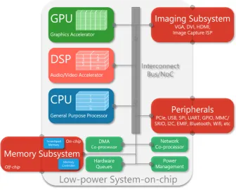
[image:31.595.155.492.439.709.2]A System-on-chip (SoC) processor is composed of multiple on-chip compute devices often with disparate Instruction Set Architectures (ISA). Each such de-vice is designed for a specialized task such as running an operating system or rendering graphics. These devices are connected together via a high speed in-terconnect such as a Network-on-chip (NoC) communication subsystem. SoC processors are used in both mobile computing devices as well as desktop and server class systems. A low-power SoC (LPSoC) such as the TI Keystone II is ex-clusively used in energy constrained mobile computing devices or in embedded computing applications. Figure 2.1 portrays a typical LPSoC processor.
Figure 2.1: A typical Low-power System-on-chip
Two key devices constituting an LPSoC include the CPU and an accelerator such as a Graphics Processing Unit (GPU) or a Digital Signal Processor (DSP). A multi-core CPU with branch prediction, coherent caches and additional float-ing point units (FPU) is designed to run an operatfloat-ing system and networkfloat-ing stack. A many-core GPU capable of running hundreds of threads simultane-ously on multiple data items is well suited to render frames used to display graphics. A multi-core DSP capable of executing Very Long Instruction Word (VLIW) instructions is suited for low-latency real-time tasks such as audio codec processing.
This thesis considers the use of both ARM and DSP cores on the TI Keystone II LPSoC for HPC. An overview of the Keystone architecture and its processing elements is provided in section 2.1. Commercial HPC systems using Keystone SoCs, including the nCore BrownDwarf considered in this thesis, are described in section 2.2.
Methods to improve the use of Single Instruction Multiple Data (SIMD) op-erations to increase code vectorization on ARM CPU cores are considered in this thesis. Section 2.3 provides a historical overview of SIMD instructions on both ARM and Intel CPUs, categorizes them in terms of functionality.
This thesis considers the use of HPC programming models, OpenMP and OpenCL, to program the Keystone II DSP cores. An overview of both OpenMP and OpenCL is provided in section 2.4 with related work on their use across other LPSoC devices.
Related work is provided in section 2.5.
2.1
The TI Keystone Architecture
The Keystone architecture from Texas Instruments is an innovative platform in-tegrating RISC and C66x DSP cores along with application-specific co-processors and input/output peripherals. It is designed with adequate internal bandwidth enabling non-blocking access to all processing cores, peripherals, co-processors and I/O subsystems.
2
.
1
.
1
The C
66
x DSP Core
Figure 2.2: The TI C66x DSP core [Texas Instruments Inc., 2010a]
Figure 2.2 presents the architecture of single TI C66x DSP Core. This VLIW DSP core has two data-paths, each capable of executing four instructions per cycle on four functional units named L, S, M, and D. The L and S units perform addition and logical operations. The M unit primarily performs multiplication operations while the D-unit performs load/store and address calculations. The two data-paths appear as an 8-way VLIW machine capable of executing up to eight instructions in each cycle.
The instruction set also includes SIMD instructions allowing vector process-ing on up to 128-bit vectors. For example, the M unit can perform four sprocess-ingle- single-precision multiplies per cycles, whereas each L and S unit can each perform two single-precision additions per cycle. Together the two data-paths can issue 8 single-precision fused multiply-add FLOPs per cycle. The double-precision ca-pability is about one-fourth of the single-precision FLOPs. This is because only two double-precision fused multiply-add FLOP are possible per cycle compared to eight single-precision multiply-add FLOPs.
2
.
1
.
2
The Keystone Memory Hierarchy
Keystone SoCs have a Non-Uniform Memory Architecture (NUMA) [Hennessy and Patterson, 2003]. A C66x subsystem can access different memory regions, with accesses to memories that are physically closer to a processor being faster. The different levels of memory and their respective configurations and access times are described below:
• Level-1 program (L1P) and data (L1D): 32KB, 1-cycle access time, config-urable as mapped RAM, cache, or a combination of mapped and cached.
• Local-L2: 2-cycle access time, configurable as mapped RAM, cache, or a combination of mapped and cached, and shared between the L1D and L1P caches.
• Multi-core Shared Memory Controller (MSMC) Scratchpad RAM (SRAM): 2-cycle access time, shared memory on-chip.
• DDR3 RAM: multiple gigabytes of off-chip memory with greater than 60-cycle access time.
2
.
1
.
3
The Keystone I SoC
The Keystone I C6678 SoC [Texas Instruments Inc., 2010b] is composed of an octa-core C66x DSP running at 1.25GHz. The DSP cores do not maintain cache coherency amongst them and virtual memory support is absent due to the lack of a Memory Management Unit (MMU).
Figure 2.3 shows the block diagram of this device. It comprises a three-tier NUMA memory hierarchy common to Keystone SoCs with 512KB of L2 memory per DSP core and 4MB of MSMC SRAM.
The Keystone I comes with a set of standard interfaces like PCI express, Se-rial Rapid I/O (SRIO), multiple Gigabit Ethernet ports as well as a proprietary interface known as the Hyperlink that provides a 50 Gbps point-to-point con-nectivity. This SoC has one DDR3 memory controller.
The DSP cores are 8-way VLIW capable of eight single-precision fused multiply-add FLOP per cycle. They have a theoretical peak performance of 20 GFLOPS per core and 160 GFLOPS aggregate single-precision GFLOPS (at 1.25 GHz). The double-precision performance of the DSP cores is approximately one fourth single-precision, 40 GFLOPS.
Figure 2.3: The TI Keystone IC6678SoC [Texas Instruments Inc., 2010b]
2
.
1
.
4
The Keystone II SoC
The Keystone II66AK2HSoC [Texas Instruments Inc., 2012] shown in Figure 2.4 is composed of a quad-core ARM Cortex-A15 (up to 1.4 GHz) and an octa-core C66x DSP (up to 1.228 GHz) connected via a 2 Tb/s TeraNet bus.
Compared to Keystone I, DSP memory sizes are increased. The DSP cores still have 32KB of L1D and L1P, however the L2 memory size is increased to 1MB and MSMC SRAM is increased to 6MB. MSMC SRAM is shared by all ARM and DSP cores. Each of the C66x DSP L1 and L2 memories remain configurable and can be partitioned into SRAM and cache as needed. The DSP cores do not maintain cache coherency amongst them, similar to the Keystone I. Virtual memory support remains absent on the DSP cores as they still lack an MMU and do not share the ARM MMU. Section 2.1.1 describes the C66x DSP core.
The ARM cores have 32KB of L1D and L1P cache per core, and share a single 4MB L2 cache. These cores are fully cache coherent. This SoC provides two 72-bit DDR3 interfaces running at up to 1600 Mhz to the DDR3 memory DIMM. The Keystone II has an additional Hyperlink interface compared to the Keystone I.
RAM, MSMC SRAM, and L2 memory segments. Each EDMA controller has 64 DMA channels which support transfers triggered by both the user and inter-rupts/events in the case of chained transfers.
The ARM cores are capable of one double-precision fused multiply-add FLOP per cycle and therefore have a peak performance of 2.4 GFLOPS per core [Rajovic et al., 2013b] and 9.6 GFLOPS aggregate double-precision GFLOPS (at 1.2 GHz). Using the NEON extensions [ARM Limited, 2009], the peak single-precision per-formance would be approximately four times the double-precision perper-formance, 38.4 GFLOPS.
The DSP cores are 8-way VLIW with two 64-bit loads/stores and four single-precision FLOPS per cycle. They have a theoretical peak performance of 19.6 GFLOPS per core and 157.2 GFLOPS aggregate single-precision GFLOPS (at 1.228 GHz). The double-precision performance of the DSP cores is approxi-mately one-fourth the single-precision performance of 39.3 GFLOPS.
The Keystone II SoC consumes approximately 9-14 Watts of thermal design power (TDP) at 55 degrees C case temperature [tip]. Taking this TDP into con-sideration, the maximum energy efficiency achievable for the DSP cores would be between 2.86 and 4.37 double-precision GFLOPS/Watt. Counting the ARM cores, this aggregate efficiency ranges between 3.49 and 5.43 double-precision GFLOPS/Watt.
2.2
Commercial HPC systems using Keystone SoCs
Two commercially available HPC systems integrated the Keystone SoCs into their nodes. These are the nCore HPC BrownDwarf [nCore HPC, 2014] system, and HPE Proliant m800 server cartridge, part of HPE’s Moonshot [HP, 2014] project.
2
.
2
.
1
The nCore BrownDwarf System
The nCore BrownDwarf system consists of nodes containing both Keystone II and Keystone I SoCs. Each node has one Keystone II connected directly to two Keystone I SoCs via Hyperlink. A maximum of 24 GB of DDR3 memory, with 8GB available to each of the three SoCs, is possible on a node. Figure 2.5(b) portrays a single BrownDwarf node.
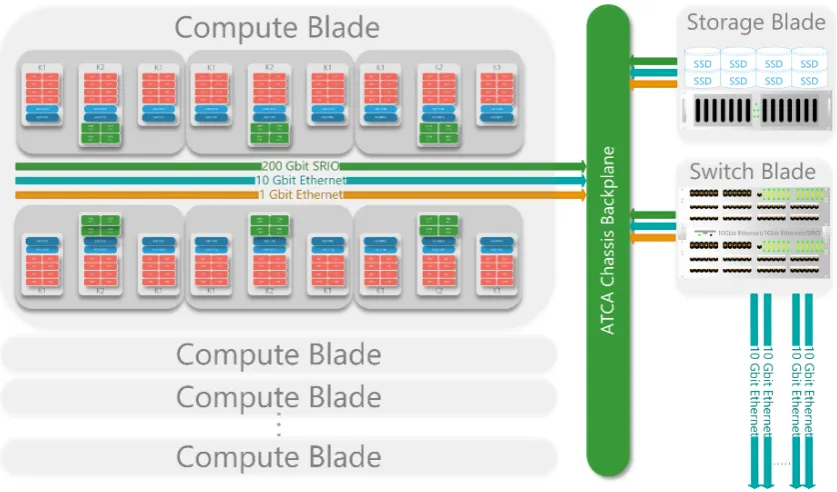
in-terconnect used for chip-to-chip and board-to-board communications. It has a theoretical bandwidth of up to 20 Gbit/sec.
A commercial off-the-shelf (COTS) PCMIG 3.0 ATCA standard chassis shown in Figure 2.5(a) is used to house BrownDwarfblades. Similar to the HPE Moon-shot cartridges, different kinds of blades are used in a BrownDwarf system. A compute blade comprises 6 nodes as shown in Figure 2.6. A storage blade provides SSD disk storage. A switch blade is used to route between the three BrownDwarf interconnection networks. Figure 2.6 presents a block diagram comprising different blades used in a BrownDwarf system. A BrownDwarf com-pute blade has the following specifications:
• 6 Processing Units (Compute Nodes or Tiles) with 1 x Keystone II and 2 x Keystone I SoCs per Unit
• 24 x ARM A15 cores @ 1.4GHz
• 144 x C66 DSP cores @ 1.2GHz
• 307.2GB/s Total Memory Bandwidth
• 156GB ECC Memory @ 1600MT/S
• 2TB/s Internal Bus
• 20Gb/s SRIO Compute Fabric (IDT SRIO SoCs)
• 7 x 10Gb Ethernet System Fabric (Broadcom Ethernet SoC)
• 1 x 1Gb Ethernet Front Panel
Any number of these blades can be combined in an ATCA chassis of the correct size to form an HPC cluster. A chassis switch connects all the blades together via the ATCA backplane in a point-to-point configuration.
2.2.1.1 Using the Hyperlink Interconnect
(a) BrownDwarf Chassis
[image:39.595.118.541.392.715.2](b) BrownDwarf Node
Figure 2.6: BrownDwarf Blade and Chassis Configuration
Hyperlink provides a point-to-point, packet-based, low latency data transfer channel. The Hyperlink protocol, similar to PCiE offers packet read, write and interrupt operations over memory mapped address ranges to a remote device from a local device.
Hyperlink has a Serializer-Deserializer (SerDes) interface but provides a more efficient encoding scheme of 8b9b compared to conventional 8b10b encoding. Between each K2 and K1 SoC there are four lanes of 10 Gbaud Hyperlink. These lanes are configured to run at a stable link rate of 6.25 Gbaud. They offer a combined theoretical bandwidth of 6.25*4*(8/9) Gbps = 22.2 Gbps = 2.78 GB/s of TX and RX between Keystone SoCs.
Hyperlink operates on 64-bit elements. Each word in Hyperlink is 64-bits and is used in two forms, either control words or data words. Each packet contains one to two control words as packet header and then followed by multiple data words.
Figure 2.7: Hyperlink Memory Transfer Window
The configuration of Hyperlink memory regions has restrictions. The size of a Hyperlink memory region must be at least 256 B and at most 256 MB. The size must also be a power of two and the region must start on a 64 KB boundary. Up to 64 memory segments are supported regardless of the total memory size. However, there is no restriction on the placement of memory regions across the entire address space. Flexible placement allows different local regions to map to different remote regions of equal size.
The BrownDwarf Hyperlink interface comes pre-configured with 64 memory regions of size 4MB. This provides an addressable window of 64×4 =256MB at a time on a remote node. In order to address a different part of the remote address space, this address window must be moved across. This is depicted in Figure 2.7.
2.2.1.2 Using a 36-bit address space with 32-bit DSP cores
Each SoC on a BrownDwarf node is attached to 8GB of DDR3 memory. Ad-dressing the 8GB requires more than 32-bits. Both Keystone ARM and DSP cores support addressing up to 36-bits. However, 36-bit addressing on the DSP cores is provided by a separate unit on the SoC rather than directly from within the DSP cores.
trans-Figure 2.8: Hyperlink Data Transfer using MPAX Address Translation
lated to the corresponding memory region in a 32-bit address space before it may be usable by a Keystone DSP. This translation is provided by the Mem-ory Protection and Address Extension Unit (MPAX) present on a Keystone SoC. MPAX provides registers that can be configured during runtime in order to map different segments of a 36-bit address space to a 32-bit address.
Figure 2.8 describes a data write operation originating from the Keystone II ARM cores using DMA engines to write to a Keystone I DSP DDR memory region on a BrownDwarf node. MPAX is used to perform address translation between 32 and 36 bit addresses in this case. First, a 36-bit source address on the ARM is mapped to a 32-bit source address using MPAX on the Keystone II SoC using akeystone_mmap()function call. A memory segment on the ARM is then mapped using Hyperlink to the remote Keystone I SoC’s MPAX registers in order to modify them.
The ARM then translates the remote K1’s 36-bit address to a 32-bit address by calling the keystone_mmap() function again, but this time with the base
address configured to be the mapped Hyperlink Segment 1. This modifies the remote MPAX to perform the address translation and designates a memory re-gion in the 32-bit address space to become the destination for the transfer.
2
.
2
.
2
The HPE Moonshot System
The HPE Moonshot project announced in 2013, comprised a number of different compute cartridges with different SoC processors composing each type of car-tridge. One such cartridge at the time was the m800. It was designed for HPC and was composed of four Keystone II SoCs as shown in Figure 2.9.
These Keystone SoCs were connected together via fast interconnects namely, TI Hyperlink and SRIO as shown in 2.9(b). Each Keystone II SoC had 8 GB of DDR3 memory and was connected externally via gigabit ethernet.
HPE used an in-house manufactured proprietary chassis that contained two types of server cartridges. The first was a compute cartridge, the m800. Recently, HPE updated their compute cartridge family [HPE, 2017] with newer SoCs such as the AMD X2150 Accelerated Processing Unit (APU), composing the m700 cartridge; or Intel Broadwell-DE and Skylake-H Xeon SoCs composing the m510 and m710x respectively. The second type was a storage cartridge providing SSD disk storage.
2.3
Single Instruction Multiple Data Operations
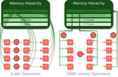
Augmenting a processor with special hardware that is able to apply a Single Instruction to Multiple Data (SIMD) at the same time is an effective method of improving processor performance. It also offers a means of improving the ratio of processor performance to power usage due to reduced and more ef-fective data movement and intrinsically lower instruction counts. This section describes characteristics of SIMD operations, how they are used and compares and contrasts the Intel SSE2 versus the ARMv7 NEON SIMD intrinsic functions. A SIMD operation acts simultaneously on multiple data elements of the same size and type (in a vector) that have already been fetched into SIMD registers. Compared to sequential or scalar processing, using a SIMD instruction can pro-vide a theoretical speed-up equal to the number of elements that can be operated on by a single SIMD instruction. This speed-up depends on the number of ele-ments of a particular data type that can be packed into a single SIMD register.
(a) Cartridge [HPE, 2013]
[image:44.595.79.499.342.696.2](b) Interconnects
On the right-hand side of Figure 2.10 the same task is performed using SIMD vector operations. In this approach a single load instruction is used to read four elements of A from memory and similarly for B. A single add instruction sums corresponding elements of A and B, with a final single store instruction used to write four elements of C back to memory. Overall, 16 separate instructions are reduced to four, giving a theoretical overall speed-up of four in the context of reduced instruction count. This notion of speed-up is simplified since it does not consider the effects of memory latency and levels of memory hierarchy that a data item needs to traverse before being operated on by a SIMD instruction.
Figure 2.10: Scalar vs. SIMD Vector Addition
The ability to load and store data as fast as possible is as critical as effec-tively operating on vectors of values using SIMD operations. This is significant given the increasing performance gap between the CPU and main memory. This problem is acknowledged in [Wulf and McKee, 1995] and is known as the mem-ory wall. This occurs when modern CPU speeds are vastly faster than resources external to the CPU chip.
as part of the instruction set included in the ubiquitous Intel x86 Complex In-struction Set Computer (CISC) processor. SIMD inIn-structions are also present in Reduced Instruction Set Computer (RISC) processors such as the SPARC64 VIIIFX [Maruyama et al., 2010] and the PowerPC A2 [Gschwind, 2012] that are used in the Fujitsu K and IBM BlueGene/Q supercomputer systems.
SIMD operations reduce the total instruction count and enable more efficient data movement which leads to increased energy efficiency [Ibrahim et al., 2009]. For example, in the context of mobile multimedia applications, audio data usu-ally exists in 16-bit data types, while graphics and video data exists in 8-bit data types. Processors used in mobile multimedia are primarily 32-bit such as the ARM Cortex-A8 and A9. Operations on 8 and 16-bit data are performed in 32-bit registers, using roughly the same energy requirements as when processing 32-bit data quantities.
By packing multiple 8 or 16-bit data types into a single 32-bit register and providing SIMD vector operations, the processor can produce multiple results with minimal increase in the required energy use. Further, as many operations are performed at once, the time for the entire computation to complete is short-ened, leading to greater reduction in the energy required to produce each result. SIMD operations are also central to heterogeneous computer systems such as the CellBE processor that was developed by Sony, Toshiba and IBM and used in the PlayStation 3 gaming console [Chen et al., 2007]. These operations are closely related to the Single Instruction Multiple Thread (SIMT) instructions supported on NVIDIA CUDA GPU systems [Kirk, 2007].
In 2009 ARM introduced enhanced floating point capabilities together with NEON SIMD technology into its Cortex-A series of microprocessors [ARM Lim-ited, 2009]. These processors were designed with the smart-phone market in mind. Inclusion of improved floating point and SIMD instructions recognized the rapidly increasing computational demands of modern multimedia applica-tions. In this environment SIMD is attractive since it leads to reduced and more effective data movement and a smaller instruction stream with corresponding power savings. The current range of Cortex-A microprocessors are capable of performing single-precision floating point operations in a SIMD fashion and have recently started supporting double-precision operations in the 64 bit ARM v8-A [ARM Limited, 2012] ISA.
2
.
3
.
1
Using SIMD Operations
intrinsic functions; and iii) compiler auto-vectorization. There exists another method to influence the generation of SIMD instructions through the use of OpenMP compiler directives. This method is fairly recent and was incorpo-rated in the OpenMP version 4.0 [OpenMP, 2007] standard released in July 2014. Given that compiler support for these directives, a mandatory pre-requisite for evaluating this technique, was non-existent during the course of this study, this method was not evaluated.
Writing low-level assembly code that use SIMD instructions and available registers is often considered the best approach for achieving high performance. However, this method is time consuming and error prone.
Use of compiler supported intrinsic functions provides a higher level of abstraction, with an almost one-to-one mapping to assembly instructions, but without the need to deal with register allocations, instruction scheduling, type checking and call stack maintenance. In this approach intrinsic functions are ex-panded inline, eliminating function call overhead. It provides the same benefits as inline assembly, improved code readability and less errors [Intel Corporation, 2007]. The penalty is that the overall performance boost becomes dependent on the ability of the compiler to optimize across multiple intrinsic function calls.
Finally, auto-vectorization leaves everything to the compiler, relying on it to locate and automatically vectorize suitable loop structures. Therefore, the quality of the compiler and the ability of the programmer to write code which aids auto-vectorization becomes essential.
2
.
3
.
2
NEON and SSE Operations
Prior to execution of SIMD compute operations, data elements of the same size and type must be fetched from memory into specific processor registers. As shown in Figure 2.10, elements A0 to A3 and B0 to B3 must fit into the special SIMD registers before the vector v operation can be performed. Vector load operation,vland store operation,vsare used to populate the registers.
Intel SSE2 operations work with 128-bit wide XMM registers and 64-bit wide MMX registers. There are eight XMM registers, XMM0-XMM7 and eight MMX registers, MM0-MM7. The newer AVX and AVX2 instruction use 256-bit wide YMM registers.
2
.
3
.
3
Intrinsic Data Types
Separate data types are defined to represent vectors used as operands in intrinsic functions. These types can only be used as parameters, assignments or return values for intrinsic functions and cannot be used in arithmetic expressions.
In C code, Intel SSE2 uses four types to represent packed data elements [Intel Corporation, 2007]: i) __m64 can hold eight 8-bit values, four 16-bit values,
two 32-bit values, or one 64-bit value; ii) __m128can hold four packed single-precision 32-bit floating point values or a scalar single-single-precision floating point value; iii)__m128dcan hold two double-precision 64-bit floating point values or a scalar double-precision floating point value; and iv)__m128ican hold sixteen 8-bit, eight 16-bit, four 32-bit, or two 64-bit integer values.
ARMv7 NEON data types [ARM Limited, 2009] are more descriptive and are named according to the pattern: < type >< size > x < number o f lanes > _t. Types representing integer data include int8x8_t, int8x16_t, int16x4_t,
int16x8_t,int32x2_t,int32x4_t,int64x1_tandint64x2_t. Unsigned
integer data is represented by similar types with uint instead of int as the
< type >. There are 2 floating point types, float32x2_t and float32x4_t, both for single-precision floating point values. NEON also provides 8 and 16-bit polynomial data types, poly8x8_t, poly8x16_t, poly16x4_t and
poly16x8_t. Further, NEON also provides data types representing arrays of
vector types following the pattern: < type >< size > x < number o f lanes > x <length o f array >_t. These types are treated as ordinary C structures. For example, int16x4x2_t represents a struct type with parameter int16x4_t
val[2]. Here,val[2]is an array of size 2 holdingint16x4_tdata.
2
.
3
.
4
Naming and classification of intrinsic functions
All intrinsic functions follow a naming convention. SSE2 intrinsics are named according to the pattern: _mm_[intrin_op]_[su f f ix]. Here, intrin_op refers to the basic operation of the intrinsic such as add orsub, whilesuffix denotes the type of data on which the intrinsic operates [Intel Corporation, 2007]. NEON intrinsics follow: [intrin_op][f lags]_[type]. The flag qdenotes that the intrinsic
is using quad-word (128-bit) Q registers [ARM Limited, 2009]. SIMD intrinsic functions can be classified under eight categories:
of vectors.
2. Arithmetic: Addition, subtraction, multiplication, absolute difference, max-imum, minmax-imum, and saturation arithmetic are provided by both SSE2 and NEON. Reciprocal and square root operations are also provided by both for floating point data. SSE2 also supports division and averaging instruc-tions for double-precision floating point data. NEON further implements different combinations of these operations such as halving add; multiply accumulate; multiply subtract; halving subtract; absolute difference and accumulate; folding maximum, minimum; operations with a scalar value; and single operand arithmetic.
3. Logical: Bitwise AND, OR, NOT operations and their combinations. Both SSE2 and NEON provide AND, OR and XOR operations. Further, SSE2 provides AND NOT operations and NEON provides NOT, bit clear, OR complement and bitwise select operations.
4. Compare: Data value comparisons =,<=,<,>=,>. Both NEON and SSE2 provide these operations. Further, SSE2 provides the 6= (neq) operation and NEON provides absolute value >,>=,<,<=operations.
5. Pack, Unpack and Shuffle: SSE2 and NEON both providesetinstructions that store data elements into vectors. NEON also supports setting individual items or lanes in vectors, and initializing vectors from bit patterns. SSE2 supports unpack and pack operations that interleave high or low data ele-ments from input vectors and place them in output vectors. NEON has similar vector extract operations. SSE2 also providesshuffleoperations that rearrange bits based on a control mask.
6. Conversion: Transformations between supported data types. Both SSE2 and NEON provide conversions between floating point and integer data types with saturation arithmetic and low/high element selection within vectors.
7. Bit Shift: Often used to perform integer arithmetic operations such as di-vision and multiplication. SSE2 and NEON both have bit shifts by a con-stant value. NEON further has bit shifts by signed variables; saturation and rounding shifts; and shifts with insert.
2.4
Programming models for Heterogeneous HPC
sys-tems
LPSoC manufacturers have clear preferences over which programming SDK they provide. Several factors dictate this. The most important factor is control over the SDK and the speed at which they can implement and push improve-ments, bug fixes and new features out to users.
Even though widely accepted and open standards of HPC programming models such as OpenMP and OpenCL have been adopted by most manufactur-ers, some choose to provide their proprietary ones such as CUDA by NVIDIA. Texas Instruments supports the OpenCL standard and provides a version 1.1 conformant runtime for the Keystone II SoC.
This work considers both OpenMP and OpenCL standards and sections 2.4.1 and 2.4.2 respectively describe the fundamental aspects of these two program-ming models.
2
.
4
.
1
OpenMP
The Open Multi-Processing (OpenMP) specification was designed primarily for shared memory programming across multi-core systems. It is a mature pro-gramming standard which was established in 1997 [Dagum and Menon, 1998]. Through the use of compiler directives specified in the OpenMP standard, it is possible to distribute sections of code orparallel regionsacross available process-ing elements.
The OpenMP 3.0 specification, released in 2008, also supported the notion of lightweight tasks that could be launched simultaneously and would be dis-tributed across available compute cores by the runtime either using a pre-defined or load-balancing scheduling policy.
The OpenMP 4.0 specification, released in 2014, added an accelerator model that enables a programmer to direct execution to heterogeneous processing ele-ments with separate address spaces. Using this model, programmers have the capability to identify the code segments that they want to run on a compute accelerator.
environ-ment to a target device data environenviron-ment. The model supports both shared and distributed memory systems between host and target devices.
Program execution begins on the initial host device. The target construct indicates that the subsequent structured block is executed by a target device. Buffers appearing in map clauses are mapped to the device data environment.
Themapclause has amap-typewhich may be specified before the list of variables. The map-type is one of to, from, tofrom and alloc and is used to optimize the mapping of buffers. Array section syntax is supported on pointer and array variables that appear in map clauses to indicate the size of the storage that is mapped.
In Figure 2.11 thetargetconstruct indicates that the subsequent structured block may execute on a target device. The array sections specified for the buffers A and B and the buffers N and sum are mapped to the target device data en-vironment. Use of the from map-type indicates that the corresponding buffer
sum on the target device is not initialized with the value of original sum buffer on the host.
Once execution begins on a target device, the iterations of the loop after the
parallel forconstruct are executed in parallel by the team of threads
execut-ing on the target device. When the targetregion is complete the value of the original buffersumon the host is assigned the value of the corresponding buffer sum on the target device and all previously mapped buffers are un-mapped.
The thread on the host device that encountered the target construct then continues execution after thetargetregion finishes execution.
1 double f(double * restrict A, double * restrict B, int N)
2 {
3 double sum;
4 #pragma omp target map(to: A[0:N], B[0:N], N) map(from:sum)
5 {
6 sum = 0.0;
7 #pragma omp parallel for reduction(+:sum) 8 for (int i=0; i<N; i++)
9 sum += A[i] * B[i];
10 }
11 return sum;
12 }
Figure 2.11: target construct
and target device share physical memory. Even if memory is shared, a pointer translation or memory coherence operation might still be required when map-ping a buffer.
The OpenMP 4.0 accelerator model supports hardware configurations with multiple address-spaces. When a buffer in a host data environment is mapped to a corresponding buffer in a device data environment, the model asserts that the host buffer and corresponding buffermayshare storage. Writes to the device buffer may alter values in the host buffer. Therefore, a program cannot assume that a mapped buffer results in a copy of that buffer being made in device memory.
Other device constructs include the target data and target update
constructs which are used to manage the placement and consistency of variables mapped to device data environments. The teamsand distributeconstructs are also added to facilitate a new type of work-sharing pattern that exploits accelerator style loop-level parallelism. These differ from previous loop-level work-sharing using thefor clause in that the for clause divides work amongst
homogeneous processing elements sharing memory, while teams and distribute clauses cater to heterogeneous sets of processing elements within an accelerator which may or may not be sharing memory.
2.4.1.1 The bare-metal OpenMP runtime library for TI C66x DSPs
TI implemented a bare-metal OpenMP runtime library for the multi-core C66x DSP using hardware queues on Keystone SoCs. The notion of being bare-metal refers to the absence of an underlying operating system. This runtime itself im-plements inter-process communication, memory allocation and other necessary mechanisms for program execution that a typical operating system would pro-vide. This runtime is used to execute OpenMP 3.0 regions on Keystone I and II DSP cores in work described in this thesis. This section describes the implemen-tation of this runtime and provides insight into an OpenMP runtime library’s internal structure.
Performance of OpenMP based applications depends heavily on the runtime library implementation. Most compilers translate OpenMP into multi-threaded code with calls to a custom runtime library, either via outlining [Brunschen and Brorsson, 2000] or inlining [Liao et al., 2006].
the compiler. An efficient runtime library which supports thread management, scheduling, synchronization, and fast use of shared memory is essential.
The basic hardware and operating environment of the DSP cores on the Key-stone I and II systems presents some special challenges when seeking to sup-port the OpenMP programming model. Notably the shared memory controller in Keystone devices does not maintain coherency between the C66x subsys-tems such as between two DSP cores, and it is the responsibility of the running program to use synchronization mechanisms and cache control operations to maintain coherent views of the memories.
Without OpenMP, application codes executing across multiple C66x subsys-tems are required to explicitly manage thread synchronization and cache coher-ence, and communicate via the shared-L2 and shared-L3 memories. A processor can transfer a data buffer to the local-L2 via a direct memory access (DMA) con-troller.
The hardware maintains L1D cache coherency with the local-L2 within each DSP core for DMA accesses. Also, the DMA transfer completion event can be used as a synchronization event between the data producer and data con-sumer. There is no virtual memory management unit (MMU), but a memory protection mechanism protects some shared memory from being accessed by a non-authorized processor.
TI provides a light-weight multi-core task dispatch API called Open Event Machine (OpenEM) which can be used to leverage hardware queues on Key-stone SoCs. OpenEM is designed to require minimal memory and CPU cy-cles [Ins, 2004]. Various types of interactions between cores, such as blocking, communication and synchronization, are implemented by OpenEM. OpenEM also provides a fast, shared, thread-safe memory management system that is used to allocate/deallocate memory in the runtime.
An understanding of the memory model used by OpenMP is fundamental to its implementation on the C66x multi-core DSP. OpenMP specifies a relaxed consistency memory model that is close to weak consistency [Hoeflinger and de Supinski, 2005]. In this model threads execute in parallel with a temporary view of shared memory until they reach memory synchronization orflushpoints in the execution flow.
At a flush point, threads are required to write back and invalidate their tem-porary view of memory. After the memory synchronization point, threads again have a temporary view of memory. Although the C66x provides shared memory, the hardware does not automatically maintain its consistency. It is the responsi-bility of the OpenMP runtime library to perform the appropriate cache control operations to maintain the consistency of the shared memory when required.
OpenMP requires that threads synchronize their local view of shared vari-ables with the global view at a set of implicit and explicit flush points defined in the OpenMP specification. The runtime performs this synchronization in software. The synchronization steps depend on whether the shared variable is placed in on-chip local memory (L2 SRAM) or on-chip/off-chip shared memory (MSMC SRAM/DDR) as follows:
• Shared variables in on-chip localscratch memory(L2 SRAM)
1. L2 SRAM on a core is accessible to external DSP cores via a global address space
2. Any updates to L2 scratch by external DSP cores are kept coherent by the memory subsystem
3. The runtime performs a write-back invalidate of L1 at all flush points.
• Shared variables in on-chip/off-chip shared memory (MSMC SRAM/DDR)
1. Shared memory regions are marked write-through
2. The runtime performs cache invalidate operations at all flush points. Since write-through is enabled shared memory has already been up-dated and there is no need to write-back data.
Consider the implementation of parallel regions. The essential parts of the OpenMP runtime library are implemented using the OpenEM API. For each parallel region, the OpenMP compiler divides the workload into chunks that are assigned to OpenEM tasks (micro-tasks) at runtime.
One of the DSP cores is treated as a master core and the other cores are worker cores. The master core runs the main thread of execution. It is responsi-ble for initializing the OpenMP runtime and starts executing the OpenMP pro-gram (main). The worker cores wait in a dispatch loop for OpenEM tasks to show up in a queue. The following steps implement a parallel region’s fork-join mechanism:
![Figure 2.2: The TI C66x DSP core [Texas Instruments Inc., 2010a]](https://thumb-us.123doks.com/thumbv2/123dok_us/1964360.157215/33.595.187.459.144.360/figure-ti-c-x-dsp-core-texas-instruments.webp)
![Figure 2.3: The TI Keystone I C6678 SoC [Texas Instruments Inc., 2010b]](https://thumb-us.123doks.com/thumbv2/123dok_us/1964360.157215/35.595.199.451.111.375/figure-the-ti-keystone-soc-texas-instruments-inc.webp)
![Figure 2.4: TI Keystone II 66AK2H SoC [Texas Instruments Inc., 2012]](https://thumb-us.123doks.com/thumbv2/123dok_us/1964360.157215/36.595.99.473.182.633/figure-ti-keystone-ii-soc-texas-instruments-inc.webp)