Int. J. Electrochem. Sci., 9 (2014) 700 - 709
International Journal of
ELECTROCHEMICAL
SCIENCE
www.electrochemsci.org
Short Communication
Drift and Diffusion Component Studies in CdTe Structure for
Photovoltaic Application
A. H. Reshak1,2,*, M. M. Shahimin3 and I. F. Fauzi3
1
New Technologies - Research Center, University of West Bohemia, Univerzitni 8, 306 14 Pilsen, Czech Republic
2
Center of Excellence Geopolymer and Green Technology, School of Material Engineering, University Malaysia Perlis, 01007 Kangar, Perlis, Malaysia
3
Semiconductor Photonics & Integrated Lightwave Systems (SPILS), Tun Abdul Razak Laser
Laboratory (TAREL), School of Microelectronic Engineering, Universiti Malaysia Perlis (UniMAP), Kampus Pauh Putra, 02600, Arau, Perlis, Malaysia.
*
E-mail: [email protected]
Received: 7 October 2013 / Accepted: 19 November 2013 / Published: 8 December 2013
A photovoltaic cell is designed to convert sunlight into electrical energy through the photoelectric effect. Solar cells are the most attractive source to harness solar energy; it is not only has high efficiency, but also protect our environment from pollution and producing zero greenhouse effect. There have been numerous studies on cadmium telluride (CdTe) compound in solar cell research. These studies have shown that CdTe can provide a good efficiency and yet be cost effective. This paper presents the investigation of cadmium telluride solar cells structure by using MATLAB software. Some important parameters such as drift component, diffusion component, thickness, and the efficiency of the cadmium telluride layer were investigated. The study concludes that in order to achieve an efficiency of 28-30%, the thickness of the CdTe layer, the uncompensated acceptor concentration and carrier lifetime should be ≥12µm, ≥1016cm-3 and ≥ 10-11s respectively.
Keywords: Photovoltaic structure, cadmium telluride, diffusion component, drift component, efficiency
1. INTRODUCTION
used in various forms, including amorphous [1], single-crystalline [2, 3], and multi-crystalline [4]. Another type of material is polycrystalline thin films, for example, copper indium diselenide (CIS) [5], cadmium telluride (CdTe) [6-8] and thin-film silicon [9]. There is also an emerging field utilizing organic material to create bulk [10] or hybrid solar cells [11, 12] with high efficiency.
Cadmium telluride have some advantages compared the others materials. CdTe have the necessary electric field, which stems from properties of two types of cadmium molecules, cadmium sulphide and cadmium telluride, which makes conversion of solar energy into electricity possible. The required properties of solar cells can be achieved through a simple mixture of those cadmium molecules, simplifying the manufacturing processes compared to the multistep process of joining two different types of doped silicon in the silicon solar panel [13]. This shows that CdTe is easier to be deposited and more suitable for large scale production. Furthermore, CdTe capture sunlight energy at shorter wavelength, stretching beyond what is possible with silicon panels. Cadmium is also easy to find, abundant and produced as a by-product of other important industrial metals such as zinc.
2. STRUCTURE AND FORMATION
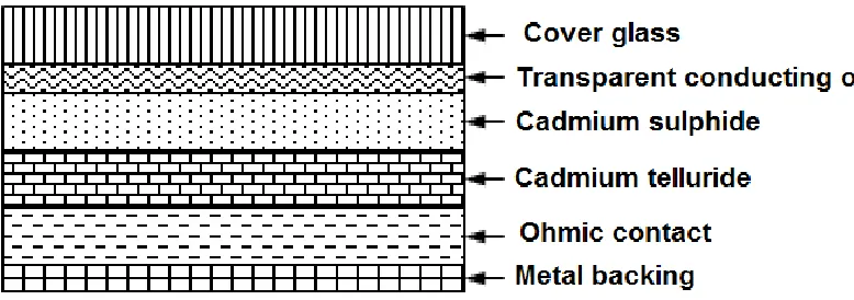
[image:2.596.92.481.398.535.2]2.1. Structure of CdTe Solar Cells
Figure 1. The structure of CdTe/CdS solar cells has a superstrate arrangement.
The structure of the CdTe solar cells has a superstrate arrangement as shown in Figure 1, with the active materials sandwiched between a cover glass and metal backing. The active materials are covered by a transparent conducting oxide (TCO) coated glass substrate as a protection from the harsh radiation environment. The TCO coated glass serves as a conductive contact to the window layer. Hence, the glass needs to have a high transparency in the visible region and a low sheet resistance [14]. The glass layer is applied to the top of the cell to reduce the reflection losses to less than 5 percent [15]. Semiconductor layers are grown on a TCA (typically stanum dioxide, SnO2) coated glass
temperature CdS and/or CdTe deposition processes since it is more stable in 450 - 550ºC region, which is for the deposition process [17]. Increasing the cover glass thickness has been known to reduce the power degradation of the solar cell [18].
Top of the active layer is an N-type, CdS or also known as the window layer as shown Figure 1. The window layer should be thin, have a wide bandgap (2.8 eV or more) in order to let all available light to the absorber layer while absorbing energy from the high-energy end of the spectrum. The absorber layer (usually doped with p-type material) must have a suitable bandgap to provide a feasible voltage and the ability to absorb photons for high current. The semiconductor in this case is cadmium telluride (CdTe), which, along with cadmium sulphide (CdS), creates the n-type and p-type layers required for the photovoltaic cell to function.
Light beam on the glass surface, passes through the front contact oxide layer and encounters a thin n-type CdS layer which is thin enough to minimize absorption without compromising the device voltage [19]. A much thicker CdTe layers have been required in order to yield devices with high solar conversion efficiency [19-21]. The thickness of the CdTe film is similarly controlled by varying deposition time. In order to increase the stability of thinner CdTe devices, aggressive etches like nitric-phosphoric (NP) need to be avoided while possibly incorporating other mechanisms like copper (Cu) oxidation as a means to reduce dopant mobility [22]. The back contact, usually made of metal, in the CdTe/CdS thin film solar cell is very important part of device fabrication. The back contact covers the entire back surface of the solar cell and acts as a conductor. Ohmic contact need to be of low resistance contact for majority carriers so it can pass the current easily. In fact, achieving low resistance back contacts remains as one of the most challenging aspects in fabricating a high performance CdTe cells.
2.2. Formation of Cadmium Telluride
There are a wide variety of methods for fabricating CdTe layer, including closed-space sublimation, electrodeposition, and chemical vapor deposition.
Closed-space sublimation
The advantage of this method is all components of the source material are directly transported to the substrate surface independently of the conditions elsewhere in the system and it also provides a high deposition rate [23].
Electrodeposition
This technique is a low cost method at low deposition rate, whereas high temperature vapor phase methods are more expensive but in return, allows high deposition rates.
Chemical vapor deposition (CVD)
2.3. Formation of Cadmium Sulphide
Heterojunction is a region of electrical contact between two different materials which have different energy bandgap and both lattice constants must be well match. This is because any lattice mismatch can introduce to dislocations resulting in interface states [24]. The heterojunction is made of two layers; top layer which acts as a window to allow light to pass through and absorbed by the bottom layer. Due to the specific roles, top layer have to be of high bandgap material, which in our case in CdS [25] and bottom layer to be low bandgap, CdTe [26]. Light shining on heterojunction generates electron-hole pairs very near to the junction. This effectively separates the electron-hole pair before recombination. There are variety of techniques in depositing CdS layer such as spray pyrolisis, thermal evaporation, chemical bath deposition and sputtering.
Spray Pyrolisis
This method requires the solution to be sprayed on a heated surface, where it reacts and forms a film of a chemical compound. It can also display a variety of morphologies from tenths of microns to hundreds of microns in size [27]. The technique is suitable for large area preparation [28].
Thermal Evaporation
Thermal evaporation is able to produce a pin-hole free films of various thickness while maintaining a good quality, adherent, uniform layer [29].
Chemical Bath Deposition (CBD)
CBD is a low material yield and produce a toxic CdS containing waste [30]. However, CBD is inexpensive and a simple process [31]. In glass based superstrate devices, the best cells are prepared with the chemical bath deposited CdS film [32].
Cadmium telluride is a low cost material compared to the others thin film such as copper indium gallium (di)selenide (CIGS) and gallium arsenide (GaAs). CIGS materials system is more complex than CdTe and has higher demands on the process control systems. For CIGS, it has to be doped with other materials to form a desired P-type but CdTe is automatically p-type doped. No dopant atoms need to be added during the film deposition process. GaAs is an expensive material, highly resistant radiation damage and unaffected by heat. This makes GaAs a perfect material for space applications and concentrator systems. However, the main issue of the CdTe solar cell is related to the toxicity of cadmium, even if proper recycling of the modules is offered by the module manufacturers.
2.4. Programming Structure
ηdrift =1 + S
Dp ∝ + W2φo − qVkT −1
1 + Dp S W2φo − qVkT −1
− exp −∝ W 1+∝ Ln
(3.1)
(3.2)
Prior to the looping function, all related constants need to be declared, where S is the recombination velocity at the CdS/CdTe interface, Dp is the hole diffusion coefficient, α is the absorption coefficient in the CdTe, k is the boltzman constant, Ln=(TnDn)½ is the electron diffusion length and W is the width of surface charge region [28-31]. In the drift component calculations, it was accepted that φo – qv = 1ev , Dp = 2cm2
/s, S = 107 cm/s and α = 150. The maximum possible value of the electron lifetime in CdTe single crystal is set to be Tn = 10-11, the electron diffusion coefficient Dn = 25 cm2/s and Boltzman constant kT = 0.0259 at the temperature 300 K. Value for α is varied between 101 and 106 to create 1500 points. The similar process is done for width space charge region, W. It is to investigate the drift component for W. Value of W is varied 0.01µm - 99µm.
For the diffusion component of the photoelectric effect in the solar cell, the surface recombination at the back surface of the CdTe layer is taken into account. Different between the drift and diffusion components is that drift component depends on the electric field applied while for diffusion component, it move using the thermal motion. Another process need to be carried out is the determination of the diffusion thickness of the CdTe absorber layer. Value of thickness, d = 1µm - 60µm. The thickness of the neutral part of the film is d–W. The summation of drift and diffusion components refers to the total photoelectric conversion in the absorber layer of the solar cell or the efficiency of solar cells.
Efficiency = ηdrift + ηdif (3.3)
Width space charge region, W is calculated via Equation 3.4,
𝑊 = 2 𝜀 𝜀𝑜 (𝜑𝑜 − 𝑞𝑣) 𝑞2 (𝑁𝑎 − 𝑁𝑑)
(3.4)
where ε = 10.6 is relative permittivity of the semiconductor, ε0 = 8.854 x 10⁻¹⁴ is permittivity of free space, q = 1.6 x10⁻¹⁹ is electron charge and Na - Nd is concentration of uncompensated acceptors in the CdTe layers. The value of Na - Nd is varying between 1016-1017 cm-3.
ηdif = αLn
α2 Ln2− 1exp −αW α Ln− SLn
Dn [cosh d − WLn − exp −α d − W + sinh d − WLn +αLn exp( −α(d − W)) SLn
Dn sinhd − WLn + coshd − WLn
3. RESULTS ANALYSIS AND DISCUSSION
Both drift and diffusion component are simulated against the absorption coefficient. Quantum efficiency of the solar cells is calculated from the summation of both drift and diffusion components. The crucial parameters need to be taken into account are; (i) free carrier and uncompensated acceptors concentrations, (ii) thickness of the CdTe layers, (iii) width space charge region and (iv) carrier lifetime.
0
2
4
6
8
10
x 10
50
0.2
0.4
0.6
0.8
1
alfa vs Drift component
D
ri
ft
C
o
m
p
o
n
e
n
t
alfa
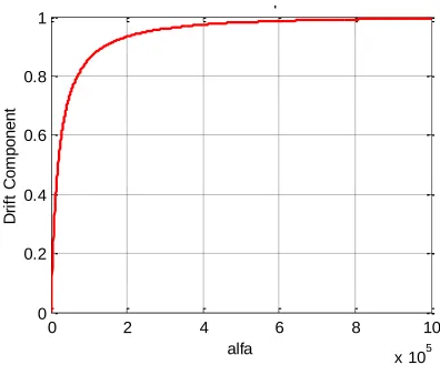
Figure 2. Drift component of the CdTe/CdS at the different absorption coefficient, α calculated at Na-Nd = 1016 cm-3, electron lifetime Tn = 10-11 and surface recombination velocity S=107 cm/s
As is seen from Figure 2, a stronger absorption coefficient near the surface indicates increment of drift component in the semiconductor. Absorption coefficient is the rate of decrease in the electromagnetic radiation intensity as light passes through a solar cell. The drift motion refers to the charged particle motion in response to an applied electric field. At the α = 5 x 10⁵
cm-1, the drift current slowly going to be saturated. The solar cell absorbs more light and the current increases correspondingly, however at maximum point, the current decreases uniformly. It is because of when light dislodging the electrons, electrons then moves freely; hence it can drift to the front contact through the CdS layer as a current.
Figure 3 represents a diffusion current increasing drastically until reached α = 1.7x105 cm-1 in the visible region. After α > 1.7x10⁵
[image:6.596.98.494.206.535.2]
the light only absorbs as much thus generating an optimum point. The optimum point at the graph shows the improvements that can be achieved by selecting specific absorption coefficient through material mixture to increase the efficiency of CdTe solar cell.
0 2 4 6 8 10
x 105 0
0.1 0.2 0.3 0.4 0.5 0.6 0.7
dataalfa vs datadff
D
if
fu
s
io
n
C
o
m
p
o
n
e
n
t
alfa
Figure 3. Diffusion component of CdTe/CdS at different absorption coefficient α calculated at Na-Nd = 1016 cm-3, electron lifetime Tn = 10-11 and surface recombination velocity S=107 cm/s.
0 2 4 6 8 10
x 105 0
0.2 0.4 0.6 0.8 1 1.2 1.4 1.6
alfa vs Efficiency
E
ff
ic
ie
n
c
y
[image:7.596.104.479.122.409.2]alfa
[image:7.596.125.470.456.744.2]
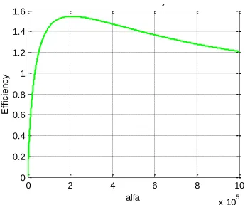
Figure 4 shows the efficiency against the absorption coefficient. The conversion efficiency increases dramatically to the peak at absorption coefficient 2.1 x 105 cm-1. This graph demonstrates the optimum value for drift and diffusion current. The ideal absorption coefficient for CdTe solar cell is 2.1 x 105 cm-1 under specified parameters stated in this paper. In the heterojunction, the absorbed solar radiation generates a free charge carriers (electron-hole pairs), which creates a current. The carriers flow towards the electrodes are done in two ways; diffusion on the outside of the solar cell and drift in the built-in electric field. The summation of both ways of carriers flow is used to obtain the efficiency of absorption coefficient. It is shows that drift current and diffusion material are important in making efficiency of the specific materials.
Factors that influence drift current are width space charge region and uncompensated acceptors. Uncompensated acceptor can be controlled by the amount of doping materials but at the same time, the width space charge region is uncontrollable. The theoretical limit of the solar to electrical energy conversion efficiency of a CdTe based device is about 28–30% [32, 33, 36]. The highest reported efficiency of a CdTe/CdS solar cell is 16.5% [32, 33, 36]. Hence, improvement to the efficiency of existing CdTe solar cells can be done via material selection of specific absorption coefficient.
4. CONCLUSION
The fabrication of CdTe is simple and cost effective in making high conversion efficiency solar cells. CdS is used side by side with CdTe as a window layer to guide light to the absorber layer. CdS/CdTe has been proven to be a good match in obtaining a high efficiency solar cell. However, so far, efficiency for CdTe/CdS solar cells is achieved around 10-16%. The study on efficiency of absorption coefficient carried out in this paper resulted in several important practical conclusions:
Drift component is obtained by utilizing Equation 3.1. It is found out that the drift component increases to the certain value and saturates afterwards. In the same time, width space charge region decreases.
Diffusion component is obtained by using Equation 3.2. It is observed that diffusion component increases to a certain value (optimum value) before decreasing with absorption coefficient. In the same time, thickness of the CdTe layer also increases.
Efficiency can be achieved around 30% with a 12µm thickness of CdTe layer, which sufficiently absorb 90% of the incident photons. In this case, the CdTe layer thickness, d should be greater than that typically used in the fabrication of CdTe/CdS solar cells (2-10µm). The 99% collection efficiency of the charge generated in the CdTe layer is achieved for d = 20-30µm.
Doping other material is the one method to increase the efficiency via improvement of the solar cell absorption coefficient. The studies carried out in this paper paved the way for further investigation in the improvement of CdTe solar cell.
ACKNOWLEDGEMENTS
UniMAP respectively, are acknowledged for the funding used for this investigation. For the author A. H. Reshak the result was developed within the CENTEM project, reg. no. CZ.1.05/2.1.00/03.0088, co-funded by the ERDF as part of the Ministry of Education, Youth and Sports OP RDI programme. References
1. A. Kiani, K. Venkatakrishnan, and B. Tan, Solar Energy, 85 (2011) 1817-1823. http://dx.doi.org/10.1016/j.solener.2011.04.020
2. A. H. Reshak, M. M. Shahimin, S. Shaari, and N. Johan, Progress in Biophysics and Molecular Biology, (2013) http://dx.doi.org/10.1016/j.pbiomolbio.2013.10.002
3. N. Johan, M. Mohamad Shahimin, and S. Shaari, in 2010 8th IEEE Student Conference on
Research and Development - Engineering: Innovation and Beyond, SCOReD 2010, December 13, 2010 - December 14, 2010, Kuala Lumpur, Malaysia. (2010) 377-380.
4. J. Yoo, J.-S. Cho, S. Ahn, J. Gwak, A. Cho, Y.-J. Eo, J.-H. Yun, K. Yoon, and J. Yi, Thin Solid Films, 546 (2013) 275-278. http://dx.doi.org/10.1016/j.tsf.2013.02.045
5. D. Diego-Vallejo, D. Ashkenasi, A. Lemke, and H. J. Eichler, Spectrochimica Acta - Part B Atomic Spectroscopy, 87 (2013) 92-99.
6. V. Krishnakumar, A. Klein, and W. Jaegermann, Thin Solid Films, 545 (2013) 548-557.
7. C. Li, J. Poplawsky, Y. Wu, A. R. Lupini, A. Mouti, D. N. Leonard, N. Paudel, K. Jones, W. Yin, M. Al-Jassim, Y. Yan, and S. J. Pennycook, Ultramicroscopy, 134 (2013) 113-125.
8. I. F. Fauzi, M. Mohamad Shahimin, and M. Mazalan, in 2010 8th IEEE Student Conference on Research and Development - Engineering: Innovation and Beyond, SCOReD 2010, December 13, 2010 - December 14, 2010, Kuala Lumpur, Malaysia. (2010) 392-396.
9. J. Sritharathikhun, S. Inthisang, T. Krajangsang, A. Limmanee, and K. Sriprapha, Thin Solid Films, 546 (2013) 383-386.
10.X. Zhang, L. Sun, W. Zheng, X. Bao, N. Wang, T. Wang, and R. Yang, Tetrahedron, 69 (2013) 9544-9550.
11.A. H. Reshak, M. M. Shahimin, N. Juhari, and R. Vairavan, Current Applied Physics, 13 (2013) 1894-1898. http://dx.doi.org/10.1016/j.cap.2013.07.023
12.R. Vairavan, M. Mohamad Shahimin, and N. Juhari, in 2011 IEEE Colloquium on Humanities, Science and Engineering, CHUSER 2011, Penang. (2011) 454-458.
13.F. Sass. (2009). A Bright Spot In A Dark Economy. Available: http://www.pddnet.com/articles/2009/10/bright-spot-dark-economy
14.G. Agostinelli, D. L. Bätzner, and M. Burgelman, Thin Solid Films, 431-432 (2003) 407-413. 15.D. Delorme. (2004). Lesson and Lab Activity with Photovoltaic Cells. Available:
http://www.ccmr.cornell.edu/ret/modules/documents/PhotovoltaicCells.pdf 16.A. Luque and S. Hegedus, 2nd ed.: John Wiley & Sons (2010).
17.A. Compaani, J. Sites, R. Birkmire, C. Ferekides, and A. Fahrenbruch, in Photovoltaics for the 21st Century: Proceedings of the International Symposium. (1999) 241.
18.S. W. Samwel, A. A. Hady, J. S. Mikhail, M. Ibrahim, and Y. S. Hanna, in First Middle East-Africa, Regional IAU Meeting. (2008).
19.S. J. Ikhmayies and R. N. Ahmad-Bitar, Solar Energy, 86 (2012) 2613-2619. http://dx.doi.org/10.1016/j.solener.2012.05.032
20.M. D. Archer and R. Hill: World Scientific (2001).
21.V. M. Fthenakis, Renewable and Sustainable Energy Reviews, 8 (2004) 303-334.
22.D. S. Albin, S. H. Demtsu, and T. J. McMahon, Thin Solid Films, 515 (2006) 2659-2668. http://dx.doi.org/10.1016/j.tsf.2006.05.042
23.T. L. Chu, S. S. Chu, S. T. Ang, and M. K. Mantravadi, Solar Cells, 21 (1987) 73-80. http://dx.doi.org/10.1016/0379-6787(87)90106-2
25.R. A. Joshi, V. S. Taur, A. V. Ghule, and R. Sharma, Solar Energy, 85 (2011) 1316-1321. http://dx.doi.org/10.1016/j.solener.2011.03.013
26.D. W. Lane, K. D. Rogers, J. D. Painter, D. A. Wood, and M. E. Ozsan, Thin Solid Films, 361–362 (2000) 1-8. http://dx.doi.org/10.1016/S0040-6090(99)00827-5
27.S. Pence, C. W. Bates Jr, and L. Varner, Materials Letters, 23 (1995) 195-201. http://dx.doi.org/10.1016/0167-577X(95)00042-9
28.J. De Merchant and M. Cocivera, Chemistry of Materials, 7 (1995/09/01 1995) 1742-1749. 10.1021/cm00057a026
29.N. Gaewdang and T. Gaewdang, Technical Digest of the International PVSEC, 14 (2004) 581-582. 30.D. Hariskos, M. Powalla, N. Chevaldonnet, D. Lincot, A. Schindler, and B. Dimmler, Thin Solid
Films, 387 (2001) 179-181. http://dx.doi.org/10.1016/S0040-6090(00)01705-3 31.J. Lee, Applied Surface Science, 252 (2005) 1398-1403.
http://dx.doi.org/10.1016/j.apsusc.2005.02.110
32.X. Mathew, J. P. Enriquez, A. Romeo, and A. N. Tiwari, Solar Energy, 77 (2004) 831-838. http://dx.doi.org/10.1016/j.solener.2004.06.020
33.L. A. Kosyachenko, A. I. Savchuk, and E. V. Grushko, Thin Solid Films, 517 (2009) 2386-2391. http://dx.doi.org/10.1016/j.tsf.2008.11.012
34.L. A. Kosyachenko, E. V. Grushko, O. L. Maslyanchuk, and X. Mathew, in Photovoltaic Specialists Conference, 2008. PVSC '08. 33rd IEEE. (2008) 1-4.
35.L. A. Kosyachenko, E. V. Grushko, and V. V. Motushchuk, Solar Energy Materials and Solar Cells, 90 (2006) 2201-2212. http://dx.doi.org/10.1016/j.solmat.2006.02.027
36.[Z. Fang, X. C. Wang, H. C. Wu, and C. Z. Zhao, International Journal of Photoenergy, 2011 (2011) 10.1155/2011/297350