International Journal of Innovative Technology and Exploring Engineering (IJITEE) ISSN: 2278-3075, Volume-8 Issue-7 May, 2019
CMOS Inverter with Second Function
J. Lakshmi Prasanna, K.Naga Jaya Lasya, M.Sohail Abbas, S.Sushmanth
Abstract: In this paper, the way to deal with plan of multifunctional computerized circuits is exhibited .It depends on reception of polymorphic hardware worldview which licenses advanced circuits to display in excess of one capacity while saving a similar structure .All things considered just segments of the circuit (gates) must be multifunctional. Singular gates have normally builtin effect to the event of a few wonders summoning the capacity change (e.g. control supply level and so on.), which implies that no devotednet is required for that reason . Besides,a first total arrangement of effectively reenacted two input polymorphic inputs were considered. These logic gates demonstrate the best parameters of all the recently distributed polymorphic entryways high information impedance and low yield impedance, brief time flag spread, low power utilization and low transistor count being utilized. Extensive variety of proposed polymorphic gates (work mixes) may acquire more proficient outcomes amid synthesis. The proposed strategy we have utilized as 180 nm technology utilizing TANNER Tools
I. INTRODUCTION
Boolean capacities might be for all intents and purposes executed by utilizing electronic doors. The accompanying focuses are critical to get it. Electronic entryways require a power supply. Gate INPUTS are driven by voltages having two ostensiblequalities,e.g.0V and 5V speaking to rational e 0 and rationale 1 separately. There is always a time delay between an input being applied and the output responding. The structure contemplations for a basic inverter circuit have been displayed in the beyond segment. In this phase, the structure of the inverter could be stretched out to address the combination of subjective advanced entryways, for example, NOR, NAND and XOR. The emphasis may be on combinational logic (or non-regenerative) circuits which have the property that when ever the yield of the circuit is identified with current information motions by using some Boolean expression (assuming that the homeless people through the rational doors have settled). No purpose full association Among yields and data sources is available. In some other class of circuits, known as consecutive or regenerative circuits to be examined in a later element of the yield isn't always just an element of the current information yet additionally of beyond estimations of the signal information. This is proficient by interfacing as a minimum one yields deliberately lower back to a few data sources. Thusly, the circuit recollects" beyond events and has a sense of history.
Revised Manuscript Received on May 06, 2019
J. Lakshmi Prasanna, Assistant Professor, Department of Electronics and Communications Engineering, Koneru Lakshmaiah Education Foundation Deemed to be University, Greenfields, Vaddeswaram, Guntur (Andhra Pradesh), India
K.Naga Jaya Lasya, B.Tech Student, Department of Electronics and Communications Engineering, Koneru Lakshmaiah Education Foundation Deemed to be University, Greenfields, Vaddeswaram, Guntur (Andhra Pradesh), India
M.Sohail Abbas, B.Tech Student, Department of Electronics and Communications Engineering, Koneru Lakshmaiah Education Foundation Deemed to be University, Greenfields, Vaddeswaram, Guntur (Andhra Pradesh), India
S.Sushmanth, B.Tech Student, Department of Electronics and Communications Engineering, Koneru Lakshmaiah Education Foundation Deemed to be University, Greenfields, Vaddeswaram, Guntur (Andhra Pradesh), India
A consecutive circuit contains a combinational cause parcel and a module that hold the kingdom. Model circuits are registers counters, oscillators, and memory. There are diverse circuit styles to actualize a given intent work. Likewise with the inverter, the normal plan measurements via which an entry way is classified contain region, velocity vitality and strength. Contingent upon the application, the accentuation might be on diverse measurements (e.G.,inelite processor, there placing tem poof superior circuits is the vital nine metricat the same time as in a battery labored circuit it's far the power dispersal). Not with standing these measurements, energy to clamor is moreover a vital idea. We will see that unique good judgment patterns (e.G., Dynamic common sense) can essentially decorate execution, however can be extra sensitive toclamor. As of overdue, control dispersal has moreover become a vital necessity and large accentuation is ready on expertise the well springs of depth and approaches to cope with manipulate manage.
Fig: 1.1 Block Diagram of Combinational Circuit
II. SECONDFUNCTION
Second function means usage of two gates in a single functionality .For second function we use polymorphic gates to design a function to reduce the area and to increase the power supply and time delay where MOS transistor exploited in a un coventional way where the circuit work determination depend just on the state of intensity supply voltage rails which is generally average for polymorphic circuits utilizing am bipolar transistor
Fig: 2.1 .Structure of NAND/XOR Gate
III. POLYMORPHICGATE
Structure of a polymorphic circuit is regularly contemplated on the entryway dimension of reflection. Simply the gates themselves have the conspicuous effect between coventional rationale and polymorphic
structure (amalgamation) techniques for polymorphic circuits, for example instructions to outline depiction in the conduct area to a portrayal in the basic space. A great deal of polymorphic circuits were planned utilizing transformative based strategies, particularly those including Cartesian Genetic Programming. Yet in addition non-transformative (conventional) design strategies were proposed.Going past the temperature sub ordinate AND/OR door, coming up next area couple of extra models of multi functionality that could be actualized in polytronics: • An advanced circuit could pass information in both of two inverse headings and play out a similar capacity or diverse capacities inthe two bearings.The methods of activity of a whole PC or other complex circuit could be changed momentarily by changing the temperature, supply voltage, or different parameter(s). • A circuit could be made to perform (at least one) concealed function(s) notwithstanding a promptly recognizable principle work. In the other mode, the circuit topologies are confined to those of field programmable transistor clusters (FPTAs). Development includes both (1) reproductions on computational models of FPTAs and (2) investigates genuine FPTAs that are built and tried in endeavors to actualize the models. The upsides of this mode are that circuits can be actualized by and by after development, and FPTA chips can be reconfigured to outline polymorphic entryways on to them, as required. The impediments of this mode are that (1) the topologies are confined and (2) at times, circuits developed assessing the non ideal qualities (e.g., nonzero "ON" protections 19 and limited "OFF" protections of transistor switches) of sensible segments can be more confused than those advanced through models of perfect parts.
IV. COMPLEMENTARY CMOS
[image:2.595.314.528.335.487.2]A static CMOS entryway is a mixture of structures rang the Pull Up Network and the Pull Down Network (PDN). The figure demonstrates a nonexclusive N input rationale door in which all statistics assets are dispersed to each the draw up and pull-down systems. The ability of the PUN is to offer an affiliation between the yield and VDD each time the yield the intent door is supposed to be 1 (in mild of the assets of data). Essentially, the potential of the PDN is to partner the yield to VSS when the yield of the intent do or is supposed to be 0.The PUN and PDN structures are developed in a very unrelated way with the give up purpose that unrivaled one of the systems is main in regular nation. Along-those strains, whilst the homeless humans have settled, a way dependably exists amongst VDD and the yield F, knowledge a excessive yield ("one"),or, alternatively, among VSS and F for a low yield ("0"). This is proportional to expressing that the yield hub is dependably a low-impedance hub in unfaltering element.
V. POLYMORPHICELECTRONICS
Polymorphic circuits peaks to particular sort of acomplicated circuit that presentations the every day ability to work in at the least two deliberately distinct modes, when superb (rationale) paintings is completed in each one of them. The structure (interconnections between individual elements in such circuit) stays unaltered forall the affordable modes/capacities.It is imperative to pressure now that the multi capability itself isn't perform edviastrategies for abusing there-configuration conspire for the real circuit shape, but rather than that the difference in conduct (reason work done) happens for some segments.
The switch of the capability might be masterminded in specific ways. It could be worthwhile (and to a few degree normal scenario for polymorphic hardware) if every phase indicates its affectability to a selected surprise in fee of the potential trade. It finally ends up being extraordinarily precious if such surprise is naturally present in the circuit like deliver voltage level, temperature and so forth.). At that factor, the circuit adjustments its capacity as in line with the ones conditions and no first rate flag (disseminated with the aid of a worldwide interconnection prepare) is predicted to manipulate this system. Such recreation plan maintains the over head paid for"extra"capacities low
VI. METHODS ANDMETHODOLOGIES
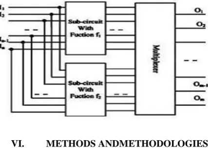
Our Proposed CMOS Technology with Second Function which means usage of two gates in a single functionality. Here we design a second function by using polymorphic gates like NAND NOR and NAND OR , where we used main function as a PMOS,NMOS Transistors. In this we can acquire some specifications like Time delay, Power dissipation . Though the normal CMOS technology cannot access a combinational logic circuits where as the Poly morphics Electronic Gates can be discussed with these modules where the different combinational circuits like Adders and Multilexers can combine and will get the single modulation of the signal
VII. DESIGNTECHNIQUES
Transistor Sizing
• Progressive Transistor Sizing
• Input Re-Ordering
• Logic Restruction
International Journal of Innovative Technology and Exploring Engineering (IJITEE) ISSN: 2278-3075, Volume-8 Issue-7 May, 2019
capacitors, This system should, there-fore, be utilized with alert. In the event that the heap capacitance is ruled by the inborn capacitance of the gate, broadening the gadget just makes a "self-stacking" impact, and the proliferation delay is un affected.
2. Progressive Transistor Sizing A substitute way to deal with uniform estimating (in which every transistor is scaled up uni-formly), is to utilize dynamic transistor .From the condition, unmistakably R1 ought to be made the littlest, R2 the following littlest, and soon. Thusly, a dynamic scaling of the transistors is advantageous: M1 > M2 >M3 > MN. Essentially, in this methodology, the vital obstruction is lessened while decreasing capacitance
3. Input Re-Ordering A few flag signals in complex combinational logic squares may be more basic than others. No tall contributions of an entryway land in the mean time. Info flag to an entryway is called basic in the event hatit is the last signal of all contributions to accept a steady esteem. Expect additionally that CL is at first charged high. On the off chance that (a),no way to GND exists until the point when M1 is turned on, which is tragically the last occasion to occur .The deferral between the entry of In1 and the yield is in this manner controlled when it take store lease CL,C1 and C2.In the second case, C1 and C2 are as of now released when In1 changes .Just CL still must be released, bringing about a littler postponement.
4. Logic Restructuring: Manipulating the rationale conditions can lessen the fan-in necessities and thus decrease the entryway delay, as outlined. The quadratic dependency of the gate delay on fan-in makes the six-input NOR gate amazingly moderate. Dividing the NOR-entryway in to two three-input entryways results in a critical accelerate, which balances by a wide margin the additional deferral brought about by handing the inverter over to a two- input NAND gate.Logic Function: The measure of progress movement is a solid capacity of the rationale work being actualized. In static CMOS entryways, the static change likelihood expecting autonomous data sources is the likelihood that the yield will be in the zero state in one cycle duplicated by the likelihood that the yield will be in the one state in the following cycle: a0 ®
1=p0•p1=p0•(1–p0)
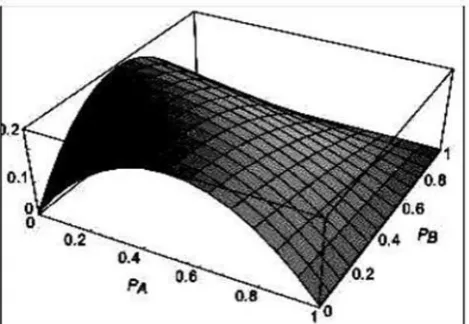
5. Signal Statistics: The exchanging movement of a rationale entryway is a solid capacity of the flag in sights. Utilizing a uniform information appropriation to register action is certifiably not a decent one since the spread through rationale entryways can essentially alter the flag insights. For 32 instance, consider by and by a 2-input static NOR entryway, and given dad and pba chance to be the probabilities that the sources of info Anand Bareone. Accept that the sources of info are not associated. The likelihood that the yield hub is a one is given by
p1 = (1-dad)(1-pb)
[image:3.595.310.545.51.213.2]The Transition Probability as an element of pa and pb. See how this diagram corrupts into the basic inverter situation when one of the information probabilities is set to 0.Fromthis plot, obviously understanding the signal measurements and their effect on exchanging occasions can be utilized to fundamentally affect the power scattering.
Fig : 7.1.Transition Activity of 2 input NOR Gate
VIII. EXPERIMENTALRESULTS
NAND-NOR
NAND-XOR
NAND-XORWAVFORMS
IX. RESULTS ANDDISUCSSION
Tab:9.2.Area and Perimeter of 4 input NAND Transistor
Transistor W AS AD PS PD
1 0.5 0.3125 0.0625 1.75 0.25
2 0.5 0.0625 0.0625 0.25 0.25
3 0.5 0.0625 0.0625 0.25 0.25
4 0.5 0.0625 0.3125 0.25 1.75
5 0.375 0.2968 0.1718 1.835 0.875
6 0.375 0.1718 0.1718 0.835 0.875
7 0.375 0.1718 0.1718 0.835 0.875
8 0.375 0.2968 0.1718 1.835 0.875
X. CONCLUSIONS
A new approach to design of multifunctional digital circuits based on polymorphic electronics The combinational of gate level mos transistors In order to reduce the number of gates to area so able amount, a very time consuming optimization has to be conducted. However, the evolutionary-based optimization procedure seems to be the only way how to obtain reasonable implementations of polymorphic circuits Here we designed the gates have high input impedance, low yield impedance, brief time of signal proliferation (generally under 1 ns), low power utilization and modest number of transistors being utilized with less area A total arrangement of two-input entryways was planned. Functionality of all the gates was verified by TANNER TOOLS. These gates show the best parameters of all recently distributed polymorphic doors More over ,smaller parts of such designed circuit scan be later enhanced at the transistor level utilizing proposed developmental streamlining
FUTUREENHANCEMENT
In this paper we constructed NAND/NOR polymorphic gate is applicable to VDD but in further we can applicable the polymorphic gate as VDD sensitive under high as well a slow temperature. Temperature range the gate function change the threshold point can be adjust at gate level to achieve the reaction of the circuit at required temperature. Future work is underway for creating and testing more complex memory-based systems such as adders, arithmetic logic units, and registers. These designs can be optimized to provide further improvements in speed, power consumption, transistor count, and reliability.
ACKNOWLEDGMENT
It is optional. The preferred spelling of the word “acknowledgment” in American English is without an “e” after the“g.”Use the singular heading even if you have many acknowledgments. Avoid expressions such as “One of us (S.B.A.) would like to thank” Instead, write “F. A. Author thanks ”Sponsor and financial support acknowledgments are placed in the unnumbered footnote on the first page.
REFERENCES
International Journal of Innovative Technology and Exploring Engineering (IJITEE) ISSN: 2278-3075, Volume-8 Issue-7 May, 2019
2. A. Stoica, R. Zebulum, and D. Keymeulen, "Polymorphic gadgets," in Int. Conf. on Evolvable Systems. Springer, 2001, pp. 291– 302. 3. C. Bobda, Introduction to Reconfigurable Computing: Architectures,
Calculations, and Applications. Springer, 2007.
4. R. Ruzicka and V. Simek, "NAND/NOR door polymorphism in low temperature condition," in 2012 IEEE fifteenth International Symposium on Design and Diagnostics of Electronic Circuits Systems (DDECS), 2012, pp. 34– 37.
5. Z. Gajda and L. Sekanina, "On transformative union of reduced polymorphic combinational circuits," JournalofMultiple-ValuedLogicfurthermore,SoftComputing,vol.17, no. 6, pp. 607– 631, 2011.
6. A. Stoica, R. Zebulum, D. Keymeulen, and J. Lohn, "On polymorphic circuits and their structure utilizing transformative calculations," in Proc. of IASTED International Conference on Applied Informatics AI2002, Insbruck, 2002.
7. V. Simek, J. Nevoral, A. Crha, and R. Ruzicka, "Towards configuration stream for spaceproficient execution of polymorphic circuits dependent on ambipolar segments," ElectroScope, vol. 11, no. 1, pp. 1– 10,2017. 8. R. Ruzicka, L. Sekanina, and R. Prokop, "Physical showing of