City, University of London Institutional Repository
Citation
:
Kim, J., Jones, K. and Horowitz, M. (2007). Variable domain transformation for
linear PAC analysis of mixed-signal systems. Paper presented at the International
Conference on Computer-Aided Design, 2007. ICCAD 2007, 05 - 08 Nov 2007, San Jose,
California, USA.
This is the unspecified version of the paper.
This version of the publication may differ from the final published
version.
Permanent repository link:
http://openaccess.city.ac.uk/2025/
Link to published version
:
http://dx.doi.org/10.1109/ICCAD.2007.4397376
Copyright and reuse:
City Research Online aims to make research
outputs of City, University of London available to a wider audience.
Copyright and Moral Rights remain with the author(s) and/or copyright
holders. URLs from City Research Online may be freely distributed and
linked to.
Variable Domain Transformation
for Linear PAC Analysis of Mixed-Signal Systems
Jaeha Kim
1, Kevin D. Jones
1, Mark A. Horowitz
1,21
Rambus, Inc., 4440 El Camino Real, Los Altos, CA 94022, USA
2Stanford University, 353 Serra Mall, Stanford, CA 94305, USA
[email protected], [email protected], [email protected]
ABSTRACT
This paper describes a method to perform linear AC analysis on mixed-signal systems which appear strongly nonlinear in the voltage domain but are linear in other variable domains. Common circuits like phase/delay-locked loops and duty-cycle correctors fall into this category, since they are designed to be linear with respect to phases, delays, and duty-cycles of the input and output clocks, respectively. The method uses variable domain translators to change the variables to which the AC perturbation is applied and from which the AC response is measured. By utilizing the efficient periodic AC (PAC) analysis available in commercial RF simulators, the circuit’s linear transfer function in the desired variable domain can be characterized without relying on extensive transient simulations. Furthermore, the variable domain translators enable the circuits to be macromodeled as weakly-nonlinear systems in the chosen domain and then converted to voltage-domain models, instead of being modeled as strongly-nonlinear systems directly.
Categories and Subject Descriptors
B.7.2 [Integrated Circuits]: Design Aids – Simulation
General Terms
Design, Algorithms
Keywords
Simulation, linear analysis, PAC analysis, domain transformation
I.INTRODUCTION
Verifying a circuit against the desired behaviors and characteristics is of critical interest to designers. To do so, designers often rely on numerical circuit simulators like SPICE [1] since accurate device model equations are too complex to solve by hand. As the circuit size grows, designers demand the higher efficiency in validating their circuits. While transient analysis in SPICE is the most versatile way of simulating the circuit response to arbitrary excitations, it is also the most time-consuming method. On the other hand, AC analysis is the most efficient way of characterizing the linear behavior of a circuit, but it can only be applied to a small class of circuits that are linear in voltage or current, such as amplifiers and filters. This paper describes a
method that can extend the AC analysis to circuits that are nonlinear in voltage or current such as phase-locked loops (PLLs) and delay-locked loops (DLLs), but that are linear in other variables such as phase, frequency, delay, or duty-cycle. With this method, the circuit’s linearized response in the chosen variables can be simulated efficiently without relying on extensive transient simulations.
It is noteworthy that many analog and mixed-signal circuits are designed to be linear in operation. In other words, these circuits strive to behave as linear systems and minimize their nonlinearities. For example, a typical design specification for a linear active filter describes the desired behavior of the filter in frequency domain, such as passband, stopband, gain, bandwidth, poles/zeros, Q-factor, etc., which are properties of a linear system. The specification also lists the measures of nonlinearities such as offset, slew rate, dynamic range, distortion, inter-modulation, etc., as quantities to be minimized to zero or maximized to infinite. Such circuits that are linear by intent can be effectively modeled as weakly nonlinear systems, as described in [13-18].
[image:2.612.326.547.595.702.2]AC analysis in SPICE is the most efficient way of characterizing the linear time-invariant (LTI) response of a circuit at a given DC bias point. AC analysis basically computes the steady-state response of the circuit to single-frequency sinusoidal excitations. Instead of simulating the response in the time domain, it first linearizes the circuit at the DC operating point and then applies frequency-domain phasor analysis to compute the response, achieving much greater efficiency in computation [2]. The responses at different frequencies are calculated simply by changing the jω-term in the complex Jacobian matrix and no iterations are required. With enough frequency points, the transfer function is obtained, which completely characterizes the linearized response of the circuit under test. That is, the transfer function can tell how the circuit responds to an arbitrary excitation, as far as the small-signal response is concerned. Therefore, AC analysis can be regarded as a formal verification method for linear
analog circuits as it can prove if the circuit has the correct linear behavior as intended. On the other hand, transient analysis can only compute the circuit’s response to one particular excitation at a time. Hence it is far less efficient in obtaining the equivalent transfer function.1
Some circuits are linear by intent in a periodically time-varying (PTV) sense and their linear responses can be efficiently characterized by periodic AC (PAC) analysis available in RF circuit simulators, such as ADS, SpectreRF, and HSPICE-RF [19,24-26]. Instead of linearizing the circuit at a DC operating point, PAC analysis linearizes the circuit over its periodic steady-state (PSS) response. The result is a periodically time-varying (PTV) transfer function described in [22,23], or equivalently a collection of LTI transfer functions between the different sidebands of the input and output signals. However, for most circuits in this category, designers are interested in only one particular LTI transfer function. For example, an up-conversion mixer is characterized by an LTI transfer function between the input baseband and the output passband (i.e. the sideband centered at the fundamental frequency of the carrier). Similarly, the main behavior of a switched-capacitor filter is characterized by the LTI transfer function between the input and output basebands. These circuits are PTV linear because they are driven by a clock that modulates their states periodically and thus have no DC steady-states.
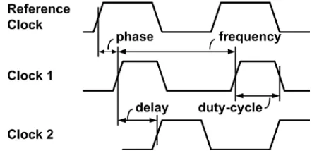
Some periodic circuits are linear by intent in variables other than voltage or current. Examples are PLLs, DLLs, and duty-cycle correctors (DCCs), which have the desired linear transfer functions expressed in phases, delays, and duty-cycles of the input and output clocks, respectively. Figure 1 illustrates various properties of a clock waveform that may be of designers’ interest. Since it is the linear transfer function that is to be measured, one might expect that the AC or PAC analysis can be applied to characterize the linear response of such systems with these non-voltage variables being the input or output.
However, AC and PAC analyses cannot directly compute the linearized response for small-signal perturbations in non-voltage/current variables. It is mainly because SPICE chooses node voltages and branch currents as state variables when it builds the state-space equation models from the circuit netlists (e.g. modified nodal analysis (MNA) described in [3]). Hence, SPICE implicitly assumes that all variables in the AC and PAC analyses are either voltage or current, and can only compute the transfer functions in voltages or currents accordingly. Besides, the circuits like PLLs and DLLs have been considered strongly nonlinear [13] since indeed they are when viewed from the voltage perspective. Thus, designers have either relied on transient analysis [8,10] and/or used component-level macromodeling approaches [6-9] to characterize the transfer functions in the desired variable domains. This paper describes a method to directly apply the PAC analysis to various variable domains. The method introduces the concept of variable domain translators, which can properly convert the perturbation in one variable to a perturbation in another. These variable domain translators enable non-voltage variables to be expressed as pseudo-voltages, so that the traditional PAC analysis
1
Some circuits are designed to be nonlinear, such as switches, logic gates, ADCs, and DACs, but note that most of the intended nonlinearities are memoryless and can be characterized by DC analysis.
can apply small-signal perturbations and measure the responses in these variables as if they were voltages. With this method, the transfer functions in the desired variable domains such as the phase transfer function of a PLL can be simulated directly and efficiently from the transistor-level circuit description. Furthermore, macromodeling these circuits that were previously considered strongly nonlinear is now more straightforward with these variable domain translators, since the circuit behavior can be first modeled as weakly-nonlinear systems in the selected variable domains, which can then be converted to the voltage domain for the macromodel to interface with the other circuits or models. The paper is outlined as follows. The next section introduces variable domain translators and discusses their requirements. Then Section III, IV, and V discuss the Verilog-A implementations of the variable domain translators and demonstrate the cases of performing AC analyses on a PLL, DLL, and DCC. Section VI highlights the benefits of this method by comparing it with the transient analysis based methods.
II.VARIABLE DOMAIN TRANSLATORS
A variable domain translator is a pseudo-circuit block that converts a quantity expressed in one domain into an equivalent quantity in another domain. For example, a phase-to-voltage translator takes a phase value as an input and produces a clock voltage waveform having the corresponding phase as the output. Similarly, a voltage-to-phase translator takes a clock voltage waveform as an input and produces its phase as the output. Note that the non-voltage quantities like phase will be treated as voltages by the simulator, since voltage and current are the only types of variables handled by SPICE-like simulators. (Verilog-A can support non-electrical variables such as phase, but they are eventually converted to voltage/current variables in the MNA matrix or internal variables inside the evaluation model.) To illustrate this, a pseudo-voltage representing a phase may have a 1V value perceived by the simulator, but it signifies 1 radian (or a scale factor can be assumed). Treating non-voltage variables as pseudo-voltages allows the circuit simulator to apply perturbations and measure the AC responses in these variables. Figure 2(a) illustrates how to perform a phase-domain AC analysis on a PLL. An AC perturbation source is applied to the input of a phase-to-voltage translator, which converts the perturbation in phase to the equivalent perturbation in the input clock waveform to the PLL. Also, a voltage-to-phase translator added at the PLL output converts the resulting perturbation in the output clock waveform to the perturbation in the output phase. After the PAC analysis, the phase-domain linear transfer function
[image:3.612.321.556.571.687.2]can be obtained by probing the AC response on the output phase pseudo-voltage node.
Variable domain translators can also help macromodel these seemingly-nonlinear circuit systems like PLLs. Since these circuits appear strongly nonlinear in voltage but are almost linear (i.e. weakly nonlinear) in the selected variable domains, it makes sense to model the circuit first as a weakly-nonlinear system in the selected variables, based on various weakly-nonlinear models described in [13-16], and then convert it to a voltage-domain model using the translators. Note that modeling the circuits directly as strongly-nonlinear systems is very difficult and only a few limited methods are known to date [17,18]. Figure 2(b) illustrates converting a phase-domain macromodel of a PLL to a voltage-domain model using the voltage-to-phase and phase-to-voltage translators. The phase-domain macromodel can be generated algorithmically from the phase-domain pseudo-circuit in Figure 2(a) [13,15-18], but we found the modified Volterra series approach outlined in [14] particularly suitable to generate the macromodels from the PSS and PAC simulation results. Here we describe the requirements for a variable domain translator to serve its purpose. A circuit with an input variable vector v and an output variable vector y can be expressed in a general nonlinear differential equation:
v y y
f( ,)= , (1)
where y denotes the time-derivative of y. In this analysis, we consider the case of an input variable domain translator, which is a pseudo-circuit block that replaces the original input variable v
with a new variable, say, φ, as shown in Figure 3. The similar analysis can be extended to the output variable domain translator which is omitted for brevity. Similar to EQ(1), we can express the translator in another nonlinear differential equation:
φ v v
g( ,)= . (2)
Then, the combination of the variable domain translator and the circuit under test results in a new system between the input φand output y, governed by:
φ y y f y y f g y y
h( ,)≡ ( ( ,),( ,))= . (3)
Note that EQ(3) is the equation used by the large-signal transient analysis [2]. Therefore, for the variable domain translator to work properly as intended in transient simulations, it must possess the correct relationship in EQ(2).
On the other hand, the PAC analysis [24-26] relies on a different circuit equation than the transient analysis. Assume that the combined system in Figure 3 has periodic steady-state (PSS) solutions of vs and ys for v and y, respectively. The PAC
analysis begins by linearizing the system around the PSS solutions based on a first-order Taylor expansion:
δφ φ y δ y h δy y h y y h S S y y + ≅ ∂ ∂ + ∂ ∂ + ) ,
( s s . (4)
Removing h(ys,ys)=φfrom both sides, we get a linear equation
between the small-signal perturbations on the input and output (δy
and δφ, respectively):
δφ y δ y h δy y h S S y y = ∂ ∂ + ∂ ∂
, (5)
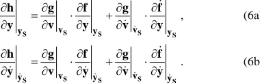
where ∂h/∂yand ∂h/∂y are Jacobian matrices evaluated at the steady-state solution (ys,ys). Based on these Jacobian matrices, the PAC analysis performs a frequency-domain analysis to compute the PTV transfer function [22,23]. By the chain rule, the Jacobian matrices of h can be expanded into sums and products of Jacobian matrices of the subcircuits f and g:
S S S S
S v y v y
y y f v g y f v g y h ∂ ∂ ⋅ ∂ ∂ + ∂ ∂ ⋅ ∂ ∂ = ∂ ∂
, (6a)
S S S S
S v y v y
y y f v g y f v g y h ∂ ∂ ⋅ ∂ ∂ + ∂ ∂ ⋅ ∂ ∂ = ∂ ∂
. (6b)
Notice that ∂h/∂yand ∂h/∂ydepend on the Jacobian matrices of the translator g, ∂g/∂vand ∂g/∂v, not necessarily on the large-signal equation g(v,v)itself. This implies that for the correct translation of perturbations between φand v, the translator must satisfy the correct relationship in:
δφ v δ v g δv v g S S v v = ∂ ∂ + ∂ ∂
, (7)
which is the small-signal perturbation equation for the translator. In summary, for the correct operation both in large-signal transient analysis and small-signal PAC analysis, the variable domain translator must satisfy two different equations, EQ(2) and EQ(7), respectively. It is important to note that satisfying one does not guarantee satisfying the other. It is especially true when implementing the translators with ideal circuit elements or in an analog behavioral description language like Verilog-A.
While Verilog-A provides a convenient way to write the behavioral description of the variable domain translators [4], it is easy to write a Verilog-A translator that has the correct operation only for the transient analysis but not for the PAC analysis. In other words, the translator has the correct relations only in EQ(2) but not in EQ(7). Figure 4 illustrates such an example for the to-voltage translator. The translator is described as a phase-modulated sinusoidal source followed by an if-statement that produces a square-wave clock for the output. One may view this if-statement as an ideal slicer as depicted in Figure 5(a), outputting one fixed value below the threshold and the other above the threshold. Since this ideal slicer has zero gains for all input values except at the threshold where the gain is infinite, it will not properly propagate the perturbation from the input to the output. As a result, this translator has an incorrect PAC response despite its correct transient response. Similar issues arise whenever a hard decision is made; for example, when using ideal switches or event triggers like @cross. Later sections describe how to resolve these issues by using smoother decision functions as depicted in Figure 5(b).
Many RF simulators including SpectreRF and HSPICE-RF require that the Verilog-A modules used in the PSS and PAC analyses be free of so-called hidden states [5]. It is because for the PSS analysis to determine if the periodic steady-state solution is reached, it must be able to access all the states in the systems. Some behavioral operators in Verilog-A imply infinite number of states which make it infeasible for the simulator to determine the
[image:4.612.356.546.192.253.2]steady state. Such operators include ideal delay operator delay and z-domain filters like zi_nd. Later sections will describe how to avoid using ideal delay elements by approximating them as finite-order continuous-time filters. While it is possible to realize a discrete-time z-domain filter as an ideal switched-capacitor filter, simulations tend to slow down significantly due to the fast transitioning edges in the sampling clock and the sampled data. It is advised that the ideal switched-capacitor filters be used sparingly to maintain fast simulation speed.
The rest of the paper describes how to perform AC/PAC analysis in various variable domains including phase, frequency, delay, and duty-cycle, with circuit examples. It also describes the Verilog-A implementations of the required variable domain translators that satisfy the above-mentioned requirements.
III.PHASE-DOMAIN AC ANALYSIS
Transforming variable domains allow us to characterize the phase-domain transfer functions of a PLL directly from its circuit netlists using the PAC analysis. Previously, the phase-domain transfer function could only be estimated based on analytical models [6,7,9], phase-domain macromodels [8], or models fitted to transient simulations [10].
Prior to PAC analysis, a PSS analysis must be performed to find the periodic steady-state solution of the PLL. The fundamental frequency for the PSS analysis is set to the lowest common divisor frequency in the system, for example, the reference frequency. Although it has been reported that the PSS convergence may consume long hours for PLLs with multiplication factors greater than 10 [8], we found that many PLL simulations can be sped up significantly by macromodeling the VCO or the divider [20,21]. Note that the PSS and PAC analyses cannot be performed on bang-bang controlled PLLs or
Σ∆ fractional-N PLLs as they do not have periodic steady states.
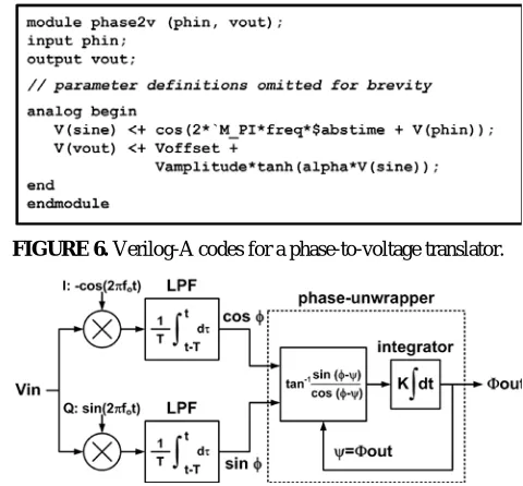
Figure 6 lists the Verilog-A code for the phase-to-voltage
translator that correctly propagates the perturbation and thus satisfies EQ(7). Notice that a tanh function is used in place of the ideal slicer in Figure 4 to sharpen the clock edges and produce a trapezoid-like clock waveform. The gain factor alpha is determined by the desired maximum edge rate of the output clock:
alpha = 1/(π·Tedge,N) (8)
where Tedge,N is the transition time normalized to the clock period.
Beware that as the gain factor alpha becomes too large, the tanh
function will start to act like an ideal slicer and stop propagating the perturbation again. For SpectreRF, we found Tedge,N value of
0.05~0.2 most appropriate.
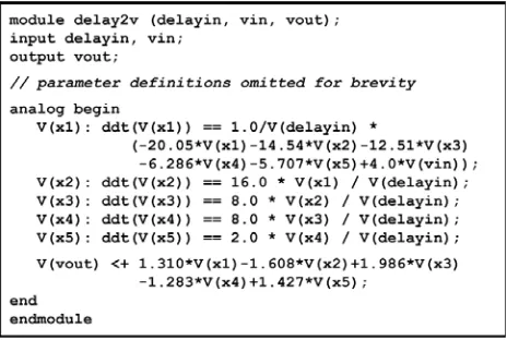
Figure 7 shows the functional diagram of the voltage-to-phase translator instead of listing the Verilog-A code for clarity. A voltage-to-phase translator is essentially a phase detector that measures the difference in phase between the input clock and the reference clock. The reference clock is implicitly assumed by the reference frequency f0 specified by the user and is generated
within the translator. While various ways of realizing ideal phase detection may exist, many of them use event triggers or hard decisions (e.g. if-statements) and thus do not properly propagate perturbations.
The translator shown in Figure 7 is based on I/Q-demodulation. First, the input clock voltage Vin is mixed with in- and quadrature-phases of the reference clock and subsequently low-pass filtered by T-long integration, where T is the clock period (=1/f0).
Therefore, the resulting signals indicate sine and cosine values of the clock phase, respectively. While one could recover the phase value by computing arctan function of the sine-to-cosine ratio, the
arctan function will cause discontinuities in its result values whenever the phase crosses the ±π boundary. To prevent this, an integrator-feedback loop is used that updates the final output phase Φout only when the intermediate phase value, φ-ψ, changes. Hence, the Φout value will always transition smoothly even when the input clock slips cycles. The ideal low-pass filter is in fact not realizable in finite-order systems and thus it was approximated as an eighth-order continuous-time filter based on a system estimation method similar to [12]. The indirect assignment
FIGURE 4. An example of a phase-to-voltage translator that does not propagate the perturbation correctly.
[image:5.612.60.294.452.552.2]FIGURE 5. Propagating perturbations through (a) a hard-decision element and (b) a soft-hard-decision element.
FIGURE 6. Verilog-A codes for a phase-to-voltage translator.
[image:5.612.315.555.476.699.2] [image:5.612.60.291.585.689.2]statement supported in Verilog-A is handy in writing the state-space differential equations [4].
Figure 8 shows the simulated phase-domain transfer functions of a PLL using the described phase-domain translators. The PLL under test was a supply-regulated PLL with an inverter-based ring oscillator, which is similar to the one described in [11]. The PLL has a multiplication factor of 1 and contains 341 active transistors in 0.13µm CMOS BSIM3 models. Figure 8(a) plots the close-loop transfer function H(jω) between the input and output phases directly measured by the PAC analysis. The open-loop transfer function G(jω) can be estimated by G(jω)=H(jω)/(1-H(jω)/N) where N is the multiplication factor. These transfer functions are highly valuable to designers as they indicate the loop bandwidth, damping factor, jitter peaking, and stability measures like phase and gain margins. Figure 8(b) plots the supply sensitivity of the PLL. The sensitivity function shows a bandpass response peaked at the loop bandwidth as predicted by [9]. It is because the low-frequency supply noise is attenuated by PLL feedback while the high-frequency noise is attenuated by the integrating function of the VCO. The low-frequency flat floor corresponds to the supply sensitivity of the output clock buffers that are not within the PLL feedback loop.
We note here that the frequency-to-voltage and voltage-to-frequency translators can also be easily implemented using the phase-to-voltage and voltage-phase translators, respectively. It is because frequency is a time-derivative of phase. As illustrated in Figure 9, a frequency-to-voltage translator is a phase-to-voltage translator preceded by an integrator that integrates the difference between the input frequency and the reference frequency. Similarly, the voltage-to-frequency translator is a voltage-to-phase translator followed by a differentiator.
IV.DELAY-DOMAIN AC ANALYSIS
Delay-locked loops are similar to PLLs except that they adjust the delay instead of the phase of the clock. We can simulate their linear transfer functions in delay domain, using the variable domain translators that convert the perturbations between voltage and delay.
A delay-to-voltage translator is basically a variable delay element that propagates the input voltage vin to the output vout with a time delay specified by the delay input delayin. Figure 10 lists the Verilog-A code for the translator. As discussed in Section II, the ideal delay operator delay available in Verilog-A language introduces hidden states that the periodic analysis cannot handle. We can instead realize the delay with a finite-order continuous-time filter. Such a continuous-continuous-time system model can be obtained by approximating the ideal delay H(jω)=exp(-jωTD) up to a
specified bandwidth, based on various system identification methods like [12]. The differential equations of the approximate delay model can be directly expressed in Verilog-A language. Figure 10 describes a fifth-order model fitted to an ideal delay, which has a delay-bandwidth product of 1.
The delay amount can be modulated by scaling the rate of change in all the state variables with the delay input. In Figure 10, notice that all the time-derivative terms (ddt) are inversely proportional to the delay input V(delayin). As V(delayin) increases, all the state variables x1, x2, …, x5 vary at the reduced rates, resulting in a longer delay. In this finite-order system, the input-to-output tracking bandwidth is inversely proportional to the delay. If a higher bandwidth is desired, one can increase the delay-bandwidth product by cascading multiple delay elements in series or by approximating the ideal delay to a higher-order system.
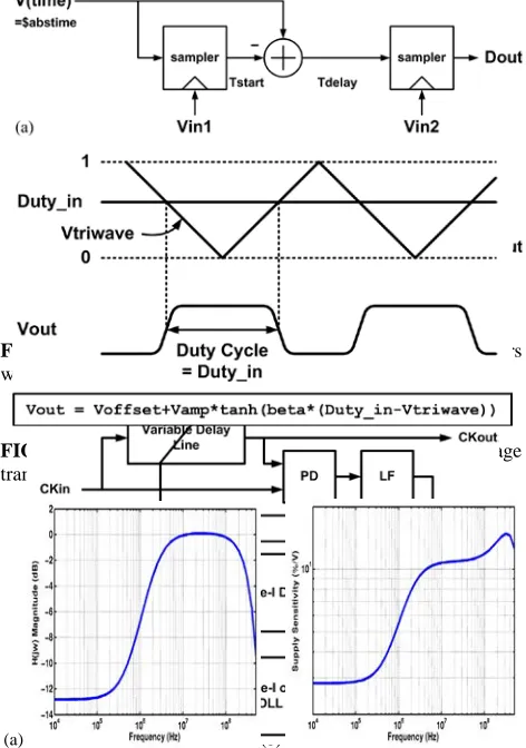
A voltage-to-delay translator takes two binary signals Vin1 and
Vin2 as inputs and produces an output Dout that corresponds to the time delay between the two input events (e.g. rising edge). Figure 11(a) illustrates a simple way of measuring the delay. Two samplers record the times at which the events occur in Vin1 and
Vin2, respectively, and the delay is the difference between the two recorded times. However, this implementation is not amenable to the periodic analysis, because the time signal V(time) continues to grow without bounds. Figure 11(b) illustrates a way to enforce a periodic steady-state solution by using modulo-T operations, where T is the period. The ramp in V(time) is replaced with a sawtooth, which is periodic in T. The samplers can be implemented as a series of two sample-and-hold switches. These ideal switches must switch smoothly to avoid problems of
(a) (b)
FIGURE 8. Simulated (a) closed-loop transfer function and (b) supply sensitivity function of a PLL.
FIGURE 9. Illustration of (a) frequency-to-voltage translator
[image:6.612.62.292.430.549.2] [image:6.612.323.555.540.696.2] [image:6.612.72.275.575.683.2]suppressing perturbations as described in Section II.
Figure 12(a) shows the block diagram of the DLL used in this example. This is a type-I DLL defined in [7], which locks the delay of the variable delay line to some fraction of the input clock period, e.g. a half. The output of the delay line CKout is compared against the input clock CKin and the difference drives the feedback loop consisting of a phase detector and a loop filter. Another type of DLL, referred to as type-II in [7], delays a separate reference clock instead of the input clock. For type-I DLLs, designers are interested both in delay-domain and phase-domain transfer functions. From the delay-phase-domain transfer function, designers check if the feedback loop is stable and has the intended bandwidth. In this case, the input delay is implicitly assumed as the input clock period. From the phase-domain transfer function, designers check if there is any excessive jitter amplification due to the latency in the feedback. Figure 12(b) and (c) show how to configure the variable domain translators to measure these different types of transfer functions.
Figure 13 plots the simulated transfer functions of a Type-I DLL in delay and phase domain. The DLL under test is again similar to the one described in [11] and was simulated with 0.25µm CMOS BSIM3 models. As expected [7], the delay-domain transfer function shows a low-pass characteristic while the phase-domain transfer function shows an all-pass with moderate amplification in
the midband.
V.DUTY-CYCLE DOMAIN AC ANALYSIS
A duty-cycle corrector (DCC) is a feedback control circuit that tries to maintain the duty-cycle of its output clock at 50%. The DCC is commonly used in systems where the rising and falling edges of the clock need to be evenly distributed; for example, data transmission based on dual-edge clocking (also referred to as double-data-rate (DDR) transmission). Figure 14 shows an analog DCC circuit tested in this example. A phase detector measures the unevenness of the rising and falling edge distribution and adjusts the control voltage Vctrl accordingly. Based on Vctrl, a duty-cycle adjuster changes the duty-cycle by skewing the up and pull-down strengths of the clock buffer chain. As with other feedback systems, bandwidth, stability, and supply sensitivity are of interest, except that the transfer functions are to be measured in the duty-cycle domain.
Figure 15 illustrates the operating principle of a duty-cycle-to-voltage translator. A clock waveform with desired duty cycle is generated by comparing a duty-cycle value Duty_in against a triangular wave, Vtriwave, which ranges between 0 and 1 and is periodic in the clock cycle. Similar to the phase-to-voltage translator case, the comparison is softened with the tanh function. The gain factor beta is again determined by the desired edge rate of the output clock: beta = 1/Tedge,N.
The voltage-to-duty-cycle translator is even simpler. First, the clock-high period is measured as the delay between the rising edge and the falling edge of the input clock using a voltage-to-delay translator, and then the output duty-cycle is computed as the clock-high period divided by the clock period.
Figure 16(a) shows the transfer function between the input and output clock duty-cycles. As expected, the transfer function exhibits a high-pass response. The DCC feedback loop is able to
[image:7.612.58.294.348.684.2]
FIGURE 11. Functional diagram of voltage-to-delay translators with (a) aperiodic and (b) periodic operation.
FIGURE 12. (a) Type-I DLL architecture; configurations for characterizing (b) delay-domain and (c) phase-domain transfer functions of a DLL.
(a) (b)
FIGURE 13. Simulated transfer functions of a DLL: (a) delay domain and (b) phase-domain.
FIGURE 15. Functional diagram of a duty-cycle-to-voltage translator.
(a) (b)
[image:7.612.378.498.434.655.2]suppress the slow variation in the input duty-cycle, but not the fast variation. The transfer function flattens in the low-frequency region, indicating the feedback loop has a finite DC gain and is unable to correct the input duty-cycle variation entirely. Figure 16(b) shows the supply sensitivity, also indicating that the DCC is effective in suppressing the low-frequency supply noise, but not as much in suppressing the high-frequency supply noise.
VI.BENCHMARK RESULTS
[image:8.612.342.531.264.392.2]This section compares the efficiencies of characterizing the linear responses using the proposed method and those based on transient analysis. To estimate the linear response in transient analysis, one can apply various test signals to the perturbation input. For example, the phase-domain transfer function of a PLL can be characterized by sinusoidally modulating the input clock phase and measuring the amplitude of the resulting sinusoidal change in the output clock phase. Since each simulation can measure only one frequency point of the transfer function, multiple transient simulations must be run with different sinusoid frequencies. A more efficient way of simulating the linear response is to measure a step or impulse response of the circuit. For example, the phase-domain step response of a PLL can be simulated by applying a step change in the input clock phase and measuring the circuit response in the output phase.
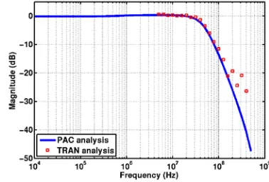
Figure 17 compares the phase-domain transfer functions measured by the proposed PAC analysis method and the transient analysis method with sinusoidal phase modulation. The results match fairly well except at high frequencies where the numerical errors due to finite time steps in transient analysis limit the smallest sinusoidal amplitude in phase that can be measured. Also, the transient simulation requires increasingly longer time to estimate the lower-frequency transfer gain as the sinusoid has a longer period.
Figure 18 compares the phase-domain step response estimated from the transfer function measured by the proposed PAC analysis and the response directly measured by the transient analysis. Generally, a good match is found between the two results as long as the applied step is sufficiently small. The step response in Figure 18 was simulated with an input phase step equal to 10% of the clock period.
Table I lists the simulation times of each method for the circuit examples discussed in this paper. The simulations were run with SpectreRF on a 3.6GHz Intel Xeon processor machine with 4GB of main memory. The results show a speed-up of 4~400×, demonstrating the efficiency of the proposed PAC analysis with variable domain transformation.
VII.CONCLUSIONS
This paper described a method to perform linear AC analysis in non-voltage domains using variable domain translators. The best candidates for this type of AC analysis are the circuits that appear strongly nonlinear in voltage domain but are linear in other variable domains, such as PLLs, DLLs, and DCCs, which are designed to be linear in phase, delay, and duty-cycle, respectively. The transfer function in the respective domain provided by the proposed analysis method completely describes the linearized response of the circuit under test and therefore formally verifies its intended behavior.
The paper derived the requirements for the variable domain translators to correctly propagate the perturbations in different variables and demonstrated their implementation in Verilog-A
analog behavioral description language. Compared to the transient-based methods, the PAC analysis combined with variable domain translators achieved the speed improvement of 4~400×. In addition, the circuits like PLLs, DLLs, and DCCs can be macromodeled as weakly-nonlinear systems in their respective domains and then transformed to voltage-domain models, instead of being modeled as strongly-nonlinear systems directly.
VIII.REFERENCES
[1] L. W. Nagel, “SPICE2: A Computer Program to Simulate Semiconductor Circuits,” Berkeley, CA: Univ. of California, Ph.D. dissertation, May 1975.
[2] L. O. Chua and P.-M. Lin, Computer Aided Analysis of Electronic Circuits: Algorithms and Computational Techniques, Englewood Cliffs, NJ: Prentice Hall, 1975.
[3] C.-W. Ho, A. E. Ruehli, and P. A. Brennan, “The Modified Nodal Approach to Network Analysis,” IEEE Trans. on Circuits
FIGURE 17. Comparison of PLL phase-domain transfer
functions estimated by the proposed PAC analysis and the transient analysis with sinusoidal phase modulation.
FIGURE 18. Comparison of PLL phase-domain step response estimated by the proposed PAC analysis and transient analysis.
[image:8.612.341.529.438.566.2]and Systems, June 1975, pp. 504-509.
[4] Open Verilog International, Verilog-A Language Reference
Manual: Analog Extension to Verilog HDL, Version 1.0,
http://www.eda.org/verilog-ams, Aug. 1996.
[5] K. Kundert, “Hidden State in SpectreRF”, http://www.designers-guide.org, May 2003.
[6] F. M. Gardner, “Charge-Pump Phase-Locked Loops,” IEEE Trans. Communications, Nov. 1980, pp. 1849-1858.
[7] M.-J. E. Lee, et al., “Jitter Transfer Characteristics of Delay-Locked Loops—Theories and Design Techniques,” IEEE J. Solid-State Circuits, Apr. 2003, pp. 614-621.
[8] K. S. Kundert, “Predicting the Phase Noise and Jitter of PLL-Based Frequency Synthesizers,” Phase-Locking in High-Performance Systems: From Devices to Architectures, New Jersey: IEEE Press, 2003, pp. 46-69.
[9] M. Mansuri and C.-K. K. Yang, “Jitter Optimization Based on Phase-Locked Loop Design Parameters,” IEEE J. Solid-State Circuits, Nov. 2002, pp. 1375-1382.
[10] J. Kim, et al., “Design of CMOS Adaptive-Bandwidth PLL/DLLs: a General Approach,” IEEE Trans. Circuits and System-II, Nov. 2003, pp. 860-869.
[11] S. Sidiropoulos, et al., “Adaptive Bandwidth DLLs and PLLs using Regulated Supply CMOS Buffers,” in Proc. IEEE Symp. on VLSI Circuits, Jun. 2000, pp. 124-127.
[12] C. P. Coelho, et al., “Robust Rational Function Approximation Algorithm for Model Generation,” in Proc. DAC, Jun. 1999, pp. 207-212.
[13] J. Roychowdhury, “Automated Macromodel Generation for Electronic Systems,” in Proc. Int’l Workshop on Behavioral Modeling and Simulation (BMAS), Oct. 2003, pp. 11-16.
[14] D. Mirri, et al., “A Modified Volterra Series Approach for Nonlinear Dynamic Systems Modeling,” IEEE Trans. Circuits and Systems-I, Aug. 2002, pp. 1118-1128.
[15] J. R. Phillips, “Projection Frameworks for Model Reduction of Weakly Nonlinear Systems,” in Proc. DAC, Jun. 2000, pp. 184-189.
[16] P. Li and L. Pileggi, “NORM: Compact Model Order Reduction of Weakly Nonlinear Systems,” in Proc. DAC, Jun. 2003, pp. 472-477.
[17] M. Rewienski and J. White, “A Trajectory Piecewise-Linear Approach to Model Order Reduction and Fast Simulation of Nonlinear Circuits and Micromachined Devices,” IEEE Trans. Computer-Aided Design, Feb. 2003, pp. 155-170.
[18] N. Dong and J. Roychowdhury, “Piecewise Polynomial Model Order Reduction,” in Proc. DAC, Jun. 2003, pp. 484-489. [19] K. S. Kundert, “Introduction to RF Simulation and Its Application,” IEEE J. Solid-State Circuits, Sep. 1999, pp. 1298-1319.
[20] X. Lai, et al., “Fast PLL Simulation Using Nonlinear VCO Macromodels for Accurate Prediction of Jitter and Cycle-Slipping due to Loop Non-idealities and Supply Noise,” in Proc. ACM/IEEE ASP-DAC, Jan. 2005, pp. 459-464.
[21] R. Batra, et al., “A Behavioral Level Approach for Nonlinear Dynamic Modeling of Voltage-Controlled Oscillators,” in Proc. IEEE Custom Integrated Circuits Conf., Sept. 2005, pp. 717-720. [22] J. Roychowdhury, “Reduced-Order Modeling of Time-Varying Systems,” IEEE Trans. on Circuits and Systems-II, Oct. 1999, pp. 1273-1288.
[23] L. Zadeh, “Frequency Analysis of Variable Networks,” Proc. I.R.E., Mar. 1950, pp. 291-299.
[24] R. Telichevesky, K. Kundert, and J. White, “Receiver Characterization Using Periodic Small-Signal Analysis,” in Proc. IEEE Custom Integrated Circuits Conf., May 1996, pp. 449-452. [25] M. Okumura, T. Sugawara, and H. Tanimoto, “An Efficient Small Signal Frequency Analysis Method of Nonlinear Circuits with Two Frequency Excitations,” IEEE Trans. Computer-Aided Design, Mar. 1990, pp. 225-235.