Rochester Institute of Technology
RIT Scholar Works
Theses Thesis/Dissertation Collections
12-1-2009
A Precise analysis of a class e amplifier
Brett Klehn
Follow this and additional works at:http://scholarworks.rit.edu/theses
This Thesis is brought to you for free and open access by the Thesis/Dissertation Collections at RIT Scholar Works. It has been accepted for inclusion
in Theses by an authorized administrator of RIT Scholar Works. For more information, please [email protected].
Recommended Citation
A Precise Analysis of a Class E Amplifier
by
Brett Klehn
A Thesis Submitted
in
Partial Fulfillment
of the
Requirements for the Degree of
MASTER OF SCIENCE
in
Electrical Engineering
Approved by:
PROF. Dr. Syed Islam
(Thesis Advisor’s Name, Printed)
PROF. Dr. Sohail A. Dianat
(Department Head’s Name, Printed)
PROF. Dr. P.R. Mukund
(Committee Member’s Name, Printed)
PROF. Dr. Jayanti Venkataraman
(Committee Member’s Name, Printed)
DEPARTMENT OF ELECTRICAL AND MICROELECTRONIC ENGINEERING
KATE GLEASON COLLEGE OF ENGINEERING
ROCHESTER INSTITUTE OF TECHNOLOGY
ROCHESTER, NEW YORK
Acknowledgements
I would like to thank my mother for all of her unyielding support through all that I have
endeavored. She has shown me through example in her own life that you can always
make a better life for yourself if you aren’t scared to take the unknown path. She has
gone out of her way to provide me with the opportunities that otherwise may not have
Table of Contents
Chapter 1: Introduction ……….. 1
1.1- Importance of Class-E Amplifiers ………. 1
1.2- Original Design by Sokal ………... 4
1.3- Recent Advances in Class-E Design ……….. 6
1.4- Motivation for this work ……… 8
1.5- Thesis Organization ………... 9
Chapter 2: Analysis ……….. 11
2.1 – Method 1: Integration Method ………. 14
2.1.1 – Accounting for OFF Transition Drain Current Decay …………. 15
2.1.2 – Drain Voltage Accounting for Decay and ON Resistance ……... 16
2.1.3 – Applying Optimal Switching Conditions ……… 17
2.1.4 – Accounting for Finite Q of the Tuned Load Network …………. 17
2.1.5 – Accounting for Finite Q of Choke Inductor LC ……… 19
2.1.6 – Applying Results of First Iteration to the Second ……… 19
2.2 – Method 2: Finite Difference Method ………. 22
2.2.1 – Defining a Gate Voltage ……….. 23
2.2.2 Defining Current Equations from KVL Loop ………. 24
2.2.3 Defining Remaining Waveforms from KCL ……….. 25
2.2.4 – Defining ON Current from Transistor Biasing ……… 27
2.2.5 – Applying Optimal Switching Conditions ……… 30
Chapter 3: Results and Discussion ………... 35
3.1 – Effects of Load Resistance and Transistor Aspect Ratio Variation ……. 36
3.2 – Varying Choke Inductor Size and Q ……… 39
3.3 – Varying Series Inductance Size and Q ………. 43
3.4 – Varying VDD ………. 45
Chapter 4: Verification of Results ………... 47
4.1 – Verification with SPECTRE® ………. 47
4.2 – Partial Verification with Hardware ……….. 51
Chapter 5: Conclusions and Future Work ……… 55
List of Figures
Figure 1.1: The complete schematic for the Class-E power amplifier. ………….……… 1
Figure 1.2: Literature reported efficiencies at different frequencies and transistor types for Class-E amplifiers. ………..………. 3
Figure 1.3: Class-E waveforms with ideal components and under optimal switching conditions as described by Sokal et al. ……….. 6
Figure 1.4: Class-E waveforms with non-ideal components and under optimal switching conditions as described by Sokal et al. ……….. 8
Figure 2.1 – a) Gate voltage, b) drain voltage, c) drain current, and d) parallel capacitor current. ………..………... 13
Figure 2.2 - Phase shift associated with the tuned network and load resistor at the first 5 harmonics. …………...………. 21
Figure 2.3 - Loop used with kirchoff’s voltage law in equations 2.17a-e. ……….. 24
Figure 2.4 - Representation of all currents entering and leaving node “a” in the circuit. 26
Figure 2.5 – a) Comparison of MATLAB and Cadence I-V curves for a device with a W/L ratio of 1500/0.6 µm. b) Comparison of I-V curves with and without accounting for short channel effects for the same 1500/0.6 µm transistor. ...………..…… 30
Figure 2.6 – Plot of eight iterations of the drain voltage. As was the case with the integral method, the solution has excellent convergence after three iterations. …………...……. 32
Figure 2.7 – Flow chart for finite difference program. ……… 34
Figure 3.1 – Variations of output power with load resistance with the transistor width as a parameter. ……… 37
Figure 3.2 – (a) ON resistance of the transistors modeled for Figure 3.1 (same parameters used). (b) Same as (a) except with larger scales on the axis. ……….. 37
Figure 3.3 – a) THD and b) efficiency as functions of the load resistance and transistor width. ………... 38
Figure 3.5 – a) Variations of the choke current waveform iLc with different choke inductors. b) Variations of output power with choke inductance with Q as a parameter. ………... 40
Figure 3.6 – Optimized circuit capacitors as a function of LC and inductor Q. ……...… 42
Figure 3.7 – a) Total Harmonic Distortion as a function of the choke inductance with Q as a parameter. The Q of LS was assumed to vary along wit the Q of LC. b) Efficiency as a function of the choke inductance with Q as a parameter. ……….… 42
Figure 3.8 – THD as a function of LS with inductor Q as a parameter. ……….. 44
Figure 3.9 – Circuit capacitor values as a function of series inductor LS with inductor Q as a parameter. Here, the Q of LC was assumed to vary with the Q of LS. ……….. 45
Figure 3.10 – Class-E amplifier a) output power, b) efficiency, c) THD, and d) circuit capacitors with variation of the power supply voltage VDD. ……… 46
Figure 4.1 – Drain current plotted for one period of the waveform. ………... 48
Figure 4.2 – Parallel capacitor current plotted for one period of the waveform. …….… 48
Figure 4.3 – Comparison of MATLAB and Cadence Class-E amplifier waveforms. a) Input voltage vGS at the gate of the transistor, b) Choke current iLc, c) Drain voltage vDS,
and d) Output voltage vO waveform. ……… 50
Figure 4.4 – I-V curves extracted form the Radio Shack® IRF-510 n-channel power MOS using a Techtronix® 571 curve tracer. ………...… 52
List of Tables
Table 1.1: Comparison of different classes of power amplifiers with respect to RF
integrated circuit performance. ……….………. 2
Table 1.2: Summary of recent advances in the design and modeling of Class-E
amplifiers. ……… 7
Table 3.1 – List of default parameters used in results presented in Chapter 3. …….….. 35
Table 3.2 – Output power and percent efficiency as functions of inductor Q. ………… 44
Chapter 1: Introduction
1.1- Importance of Class-E Amplifiers
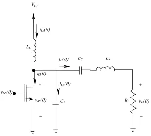
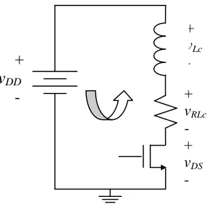
The Class-E amplifier was first introduced by Sokal et al. [1] in 1972. The Class-E
amplifier, as shown in Figure 1, was introduced as a narrow-band tuned RF amplifier
with a similar topology to that of a standard low noise amplifier (LNA), but with the
transistor acting as a switching element instead of as a voltage controlled current source
device. Under ideal conditions (infinite loss-less inductors, transistor acts as an ideal
switch, and zero fall time of the drain [or collector] current), the Class-E amplifier can be
designed to have 100% efficiency [1], making it well suited for portable RF devices such
as cell phones and wireless laptop Ethernet connections.
vGS(θ)
LC
CP
CS LS
R vO(θ) +
−
iD(θ)
iCp(θ)
iO(θ)
VDD
iLc(θ)
vDS(θ)
+
[image:9.612.165.475.381.660.2]−
A Class-E amplifier can not be used for wide band amplification, making it well suited
for only a select group of applications requiring high frequency narrowband operation.
Currently, the most common use of a narrowband high frequency amplifier is to amplify
a high frequency carrier signal that is modulated within a narrowband around the carrier
signal with a data signal. This type of signal is commonly found in IEEE wireless
standards for data transmission such as 802.11N and WiMAX (802.16), and cellular
broadcast. These applications, however, in recent years have had an exponentially
growing commercial market with the wide adoption of cellular telephone
communications and wireless networking. As portable applications continue to become
more complex, battery size and lifetime have been a growing concern. For this reason,
finding a highly efficient (amount of data throughput per unit of energy) output stage for
the transmitter is becoming an increasingly important issue. Since the frequency of
operation and data throughput are typically determined by the appliction, the power
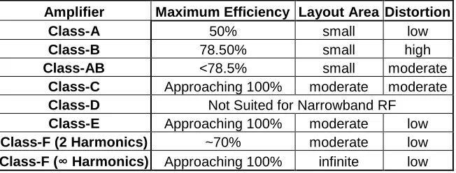
[image:10.612.109.435.530.654.2]efficiency will be reported in table 1.1 as the efficiency metric for comparison.
Table 1.1: Comparison of different classes of power amplifiers with respect to RF integrated circuit performance.
Amplifier Maximum Efficiency Layout Area Distortion
Class-A 50% small low
Class-B 78.50% small high
Class-AB <78.5% small moderate
Class-C Approaching 100% moderate moderate Class-D Not Suited for Narrowband RF
Class-E Approaching 100% moderate low
Class-F (2 Harmonics) ~70% moderate low
It can be argued that the most important issues considered when deciding on an output
stage would be obtainable efficiency, required layout area, and the amount of distortion
that would be present at the output. Table 1.1 shows a comparison of the different classes
of power amplifiers and their performances with regard to RF communications. As can
be observed from Table 1.1, a Class-E amplifier is well suited for narrowband RF
systems. It is important to note that the efficiencies presented above are only valid for
ideal components under ideal conditions, and will vary greatly with design. Reported
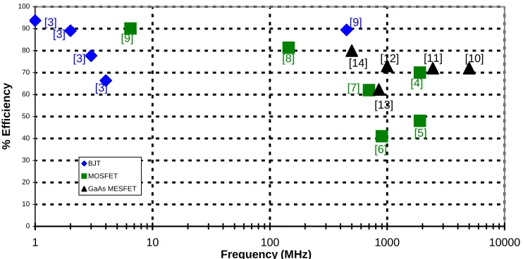
efficiencies at different frequencies for Class-E amplifiers are presented in Figure 1.2 as a
reference. As can be seen from Figure 1.2, real amplifiers are operating far enough from
100 percent efficiency so as to require an optimized design process that accounts for
non-ideal components and non-non-ideal conditions (such as imperfect gate driving voltage) needs
to be implemented. Many of the non-idealities have been accounted for individually
previously, but a complete analysis for a Class-E amplifier has not yet been presented,
and will be the focus of this thesis.
0 10 20 30 40 50 60 70 80 90 100
1 10 100 1000 10000
Frequency (MHz)
%
E
ff
ic
ie
n
c
y
BJT MOSFET GaAs MESFET
[14] [12] [11] [10]
[13] [8]
[3] [3]
[3]
[3]
[5] [4] [9]
[image:11.612.118.489.480.664.2][6] [7] [9]
1.2 – Original Design by Sokal
Sokal et al. [1] performed the original design of the Class-E amplifier assuming ideal
passive components and an ideal switching transistor. These approximations lead to the
following conditions in the amplifier:
1) Choke inductor current iLc will be a DC signal,
2) The output current iO will be a perfect sinusoidal waveform, and
3) The transistor will turn instantly ON and OFF with zero ON resistance and
infinite OFF resistance.
Under these conditions, if the drain voltage and the drain current are never both non-zero
at the same time, then no power will be consumed by the transistor, and with ideal
passives, the amplifier will operate at 100% efficiency. In order for this to occur, Sokal
et al. stated that the drain voltage and its derivative (the parallel capacitor current iCp
times a scalar as shown in equation 1.3) should both be zero at the instant that the
transistor turns ON. The voltage must be zero at the time the transistor turns on to
prevent power loss, and the derivative should be zero to allow for slight mistuning of the
amplifier [1]. These two conditions have remained as the standard optimal switching
conditions for analytical models being developed even today, and will be discussed in
greater detail in Chapter 2. From the above assumptions, the choke current and the
output current can be defined as
(
ω
+
φ
)
=
=
t
R
a
i
I
i
o
DC Lc
where a is the amplitude of the output voltage, R is the output load resistance andφ is the
phase shift between the output voltage and the input signal at the transistor gate. Using
KCL at the drain of the transistor yields the equation
o D Cp
Lc
i
i
i
i
=
+
+
. [1.2]Since the transistor and the parallel capacitor CP are in parallel, when the transistor is
ON, no current flows through Cp. However, when the transistor is OFF, zero can be
substituted into eq. 1.2 for iD with the results of eq. 1.1 yielding
(
ω
+
φ
)
−
=
=
t
R
a
I
i
i
DC Cp Cpsin
0
. [1.3]
Substituting the results of eq. 1.1 into eq. 1.2 along with the result that iCp=0 in the ON
state yields the drain equations of
(
)
0
sin
=
+
−
=
D DC Di
t
R
a
I
i
ω
φ
. [1.4]
Knowing that a current flowing into a capacitor produces a voltage and knowing that the
parallel capacitor voltage is the same as the drain voltage yields the following equation
for the drain voltage vDS
(
)
(
)
( )
+
+
−
=
−
+
=
=
∫
∫
= =φ
ω
φ
ω
ω
φ
ω
cos
cos
1
sin
1
1
0 0R
a
t
R
a
t
I
Cp
v
dt
t
R
a
I
Cp
dt
i
Cp
v
DC DS t t DC t t Cp DS. [1.5] [ON]
[OFF]
[ON]
The waveforms for these equations can be seen in Figure 1.3. For Figure 1.3, it was
assumed arbitrarily that the transistor is ON for 0≤ωt≤π , and OFF for π ≤ωt ≤2π.
Figure 1.3: Class-E waveforms with ideal components and under optimal switching conditions as described by Sokal et al.
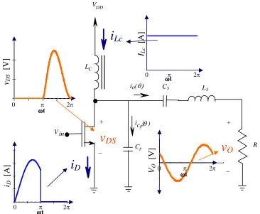
1.3 – Recent Advances in Class-E Design
The simplest modification to make to the ideal Class-E analysis is to account for the
decay in the transistor at the transition from the ON state to the OFF state. As shown in
Figure 1.3, ideally this transition is instantaneous, but in the non-ideal case there is a
decay associated with this transition. Kazimierczuk [3] has modeled this as a linearly
sloped decreasing line during the OFF state, while Tu et al. [15] have more accurately
modeled it as an exponential decay in this region which is the approach that will be used
`
Vin
LC
Cp
CS LS
R +
−
iCp(θ) iO(θ)
VDD
−
+
v
Ov
DSi
Di
Lc0 π 2π
0 π 2π
0 π 2π
0 π 2π
ωωωωt
ωωωωt ωωωωt
ωωωωt
vD
S
[
V
]
VO
[
V
]
iD
[
A
]
ILc
[
A
[image:14.612.137.503.159.460.2]in chapter 3. Neither of these papers however completely account for a non-ideal
transistor in the fact that they both assume zero ON resistance. The issue of the ON
resistance has been addressed by Choi et al. [16], Wang et al. [17], Sekiya et al. [18],
Kessler et al. [19], Reynaert et al. [20], and Alinikula et al. [21], although none of these
authors have accounted for the transistor decay time. Kessler et al. [19], Alinikula et al.
[21], and Reynaert et al. [20] however, have accounted for the parasitic resistances of the
passive components, while Reynaert et al. [20] have also accounted for the finite Q of the
output along with Tu et al. [15] and Sekiya et al. [18]. With finite output Q, the load
network will not operate as an ideal filter, and additional harmonics besides the
fundamental frequency will be present at the output as seen in Figure 1.4. Wang et al.
[17], Sekiya et al. [18] and Reynaert et al. [20] have also accounted for the finite filtering
value of the choke inductor LC. This has the effect of allowing ripple to be introduced
onto the iLc waveform as seen in Figure 1.4. A table summarizing the contributions of
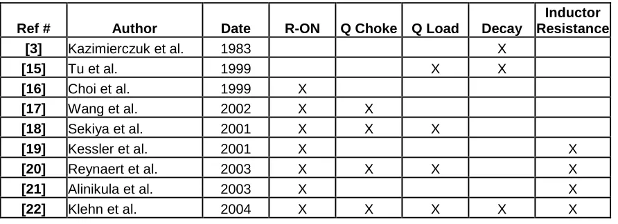
[image:15.612.107.553.536.698.2]these authors is presented in Table 1.2.
Table 1.2: Summary of recent advances in the design and modeling of Class-E amplifiers.
Ref # Author Date R-ON Q Choke Q Load Decay
Inductor Resistance
[3] Kazimierczuk et al. 1983 X
[15] Tu et al. 1999 X X
[16] Choi et al. 1999 X
[17] Wang et al. 2002 X X
[18] Sekiya et al. 2001 X X X
[19] Kessler et al. 2001 X X
[20] Reynaert et al. 2003 X X X X
[21] Alinikula et al. 2003 X X
Figure 1.4: Class-E waveforms with non-ideal components and under optimal switching conditions as described by Sokal et al. [1].
1.4 – Motivation for this work
These authors have shown that each of these non-idealities has an effect on both the
circuit performances such as efficiency and distortion, and the required circuit
components needed to meet the optimized switching conditions as defined by Sokal et al.
[1]. However, up till now, a concise analysis to account for all of these non-idealities at
the same time has not been presented. The goal of this thesis is to present an analysis that
while accounting for all these non-idealities, also plots the non-ideal waveforms,
calculates the required passive components for optimized switching conditions, and
`
V
in
L C
Cp
Cs Ls
R +
−
i C1
( θ )
i O ( θ)
V DD
−
+
v
Ov
DSi
Di
Lc0 π 2π
0 π 2π
0 π 2π
0 π 2π
ωωωωt
ωωωωt ωωωωt
ωωωωt
vD
S
[
V
]
VO
[
V
]
iD
[
A
]
ILc
[
A
measures the circuit performances through the use of a MATLAB simulation. The
analysis, presented in Chapter 2, will account for:
1) Exponential decay angle of the transistor OFF transition dependant on the gate
input voltage.
2) A variable ON resistance of the transistor dependant on the instantaneous bias
conditions of the transistor (gate and drain voltage).
3) Parasitic resistance of the two circuit inductors.
4) Finite loaded Q for the tuned output network resulting in harmonics being passed
to the output waveform.
5) Finite value of the choke inductor LC resulting in harmonics being present on the
choke current iLc.
Results of varying important design parameters such as transistor aspect ratio and
inductor sizes and the effects of such variations on circuit performances and optimized
component values is presented in Chapter 3.
1.5 – Thesis Organization
The organization of this thesis will be as follows:
Chapter II will discuss two methods for calculating the circuit parameters and waveforms
of the class E amplifier. The first method will be an integral method that will account for
finite choke inductances, drain current fall time, and loaded quality factor of the output
network inductance. The second method discussed will use a finite difference solution
resistance of the switch, rise and fall time of the input signal, and parasitic resistances of
both circuit inductors. Chapter III will discuss in greater detail the effects of the
non-ideal components accounted for in chapter II as well as the circuit power supply voltage
will have on desired circuit parameters such as efficiency, output power, and total
harmonic distortion (THD). Chapter IV will demonstrate the accuracy of the equations
presented in chapter II by comparing the results of those equations as calculated using
MATLAB® vs a commercial circuit simulator (SPECTRE®). An actual class E
amplifier is then constructed using discrete components and the output of this circuit is
compared to the equations of chapter II as calculated using MATLAB®. Chapter V has
conclusions from the presented work as well as discussion on possible future research
Chapter 2: Analysis
Two methods have been successfully implemented to simulate the class-E amplifier
waveforms, optimize the required circuit components, and calculate amplifier
performances such as efficiency and total harmonic distortion (THD). The first optimizes
the circuit parameters while considering finite choke inductances, drain current fall time,
and loaded quality factor of the output network inductance. The second accounts for all
these in addition to a finite ON resistance of the switch, rise and fall time of the input
signal, and parasitic resistances of both circuit inductors. The first method has been
published in the International Symposium on Circuits and Systems (ISCAS) 2004
conference [22], while the second method is more accurate and accounts for more
non-idealities presenting a more general solution.
The first method (integral method) utilizes an iterative technique where each waveform is
defined symbolically and solved using the integral function in MATLAB. The output
current iO and the choke current iLc are initially assumed, as well as the size of the two
inductors, and the capacitor current iC and the drain voltage vDS are calculated. From
these waveforms, a new output current and choke current are obtained which are
considered as inputs to next iteration. During each iteration, the two capacitors CP and CS
are calculated so that the switching conditions as described by Sokal et al. [1] are met.
These conditions include the drain voltage and the capacitor current both are zero at the
time when the transistor first turns on. This method assumes a constant ON resistance for
turns off (the ideal case assumes an infinitely sloped instantaneous turn off [see Figure
1.3]). This methodology also accounts for the effects of the finite choke inductance and
its effect on the amount of ripple on the “DC” supply current, and also accounts for the
finite Q of the load network (See Figure 1.4 to observe the effects of these non-idealities).
The load network acts as both a phase shifting element by tuning it slightly below the
operating frequency so it appears slightly inductive, and also as a band-pass filter passing
the first harmonic, but blocking all others in the ideal case. By taking this as a
non-infinite inductor, additional harmonics at the output are accounted for and THD can be
accurately calculated.
The second method (finite difference method) expresses the circuit equations using
differential equations and solves them simultaneously using finite difference technique.
If the waveform starts at the point where the transistor turns ON, then the initial points on
the waveforms are known from the aforementioned optimal switching conditions
described by Sokal et al. [1] as seen in Figure 2.1. From the initial points, the subsequent
points can be calculated. This method converges much faster than the integral method
while accounting for more non-idealities. The transistor is now modeled more accurately
by first defining the gate voltage similar to that of a typical Class-F driving stage (most
generic waveforms will also be accepted by the program), and then calculating the region
of operation and drain current of the transistor at each time step based on the gate voltage
at that time. In this way, the decay of the drain current at the instant when the transistor
inputs to the program including channel carrier mobility (µeff), oxide capacitance per unit
area (Cox), and threshold voltage (VT). This enables the program to accurately account for
the non-zero ON resistance of the transistor at all time steps based on the bias conditions.
The finite inductances are still accounted for, with the addition of a resistance term added
in series with the inductors to model low Q conditions similar to those found through the
use of silicon fabrication [20].
radians G a te V o lt a g e radians D ra in V o lt a g e
(a) (b)
radians D ra in C u rr e n t radians P a ra ll e l C a p a c it o r C u rr e n t
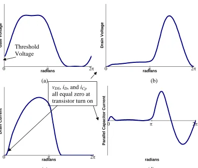
[image:21.612.121.518.281.618.2](c) (d)
Figure 2.1 – a) Gate voltage, b) drain voltage, c) drain current, and d) parallel capacitor current. Setting t=0 at transistor turn on gives knowledge of initial conditions for these waveforms based on design for optimal switching conditions.
Threshold Voltage
vDS, iD, and iCp all equal zero at transistor turn on
0 π 2π
2.1 – Method 1: Integration Method
As mentioned previously, the first iteration of the integration method starts by assuming a
symbolic waveform for the output current (iO) and the choke current (iLc) from which the
drain voltage (vDS), parallel capacitor current (iCp), drain current (iD), and new solutions
for iO and iLc are calculated. The initial waveform for the output current will be assumed
to be
(
ω +φ)
= t
R a
iO sin (2.1)
where a is the amplitude of the output voltage, R is the output resistance, and φ is the
initial phase shift of the fundamental frequency at the output. The choke inductor current
(iLc) will be assumed to have no harmonics for the first iteration and will be defined
simply as IDC1 to represent the DC level of the first iteration.
Using KCL at the drain node of the transistor, we find that
o Cp D
Lc i i i
i = + + . (2.2)
When the transistor is OFF (0≤ωt≤π ), it is assumed that no current is passing through it, therefore, solving for iCp yields,
o Lc
Cp i i
i = − 0≤ωt ≤π. (2.3)
When the transistor is ON (π ≤ωt ≤2π), assuming the ON resistance on the transistor is small in comparison to the impedance of the capacitor, the capacitor is essentially shorted
out, leaving no current through it allowing the drain current to be defined in this region as
o Lc
D i i
2.1.1 – Accounting for OFF Transition Drain Current Decay
In order to account for the exponential decay in the drain current when the transistor turns
OFF, an additional term must be added to the drain current, and since iDand iCp must still
add up to iLc-iO which are already defined, iCp must also be modified accordingly giving
the final equations
0
t
D C
D Lc o
i I e
i i i
ω τ − ⋅
= ⋅
= − π ω π
π ω 2 0 ≤ ≤ ≤ ≤ t t
and, (2.5)
0
0
t
Cp Lc O C
Cp
i i i I e
i
ω τ − ⋅
= − − ⋅
= π ω π
π ω 2 0 ≤ ≤ ≤ ≤ t t
and, (2.6)
where IC0 is the magnitude of iCp at ωt =0, (also the value of iD at ωt =2π ) in the absence of an exponential. If the transistor were a perfect switch, the drain current would
instantaneously go from IC0 to 0 at the time that the transistor transitions from the ON
state to the OFF state. In addition, the parallel capacitor current would instantaneously
go from 0 to IC0 as the capacitor becomes the new path for the current. In the presence of
a non-ideal switch, the exponential decay of the transistor channel current makes the ON
to OFF state transition of both terms more gradual. The magnitude of the exponential is
then defined as
) sin( 0 ϕ R a i
IC = Lc −
. (2.7)
It is important also to note that τ is a variable used to adjust the angle of the decay of the
exponential. The decay angle is defined as the phase when the exponential decays three
time constants from its original value. Knowing the decay angle of the transistor will
allow an easy calculation of τ for implementation in the model by using [OFF] [ON]
3 τ
ψ
= (2.8)
where ψ is the decay angle of the transistor. For reference, a 30 degree decay angle is
represented when τ is set to 5.9 and a 60 degree decay angle is represented with τ set to
2.95.
2.1.2 – Drain Voltage Accounting for Decay and ON Resistance
Knowing the current through the capacitor as a function of time allows for calculation of
the voltage introduced across it during the period that the transistor is OFF (0≤ωt ≤π ), which is also the voltage across the drain of the transistor. When the transistor is ON
(π ≤ωt≤ 2π ), it is assumed that the capacitor current is zero, so the only voltage at the drain will be produced by the current iD through the ON resistance of the transistor.
These waveforms are represented for the period defined as 0≤ωt ≤πin the equations
(
)
( )
0 0 1 0 1 1 1 cos cos t DS Cp t CDS DC C
v i dt
Cp
I
a a
v I t t I e
Cp R R
ω τ
ω φ φ
ω τ ω τ
− ⋅ = ⋅ = ⋅ − + − ⋅ ⋅ + +
∫
(2.9)and are represented for the period defined as π ≤ωt≤2π as
(
)
ONDC DS ON D DS R t R a I v R i v ⋅ − + = ⋅ = φ ω sin
1 (2.10)
Note that the equation 2.9 has additional terms when compared to equation 1.5 after
accounting for non-ideal components. It is also important to note that the assumption of
is a limitation of the integral method, and will be properly accounted for in the finite
difference methodology.
2.1.3 – Applying Optimal Switching Conditions
The unknowns at this point in the analysis are Cp, a, φ, and IDC1. Initial values were
assigned in the program for each of these parameters. Using these initial values and the
equations previously defined, accurate calculation of Cp, a, and φ can be performed. It is
known through the optimal switching conditions that vDS and iCp should both be zero at
ωt=π. The value of φ will be set to make vDS equal to zero using the approximate initial
values for the other parameters. From equation (2.2), and knowing that iCp and iD are
both zero at ωt=π, we can now say that iLc=iO, and with φ known, a is the only unknown
in that equation. It is also known that with no power consumed in the inductor, the
average voltage at vDS should be the same as the power supply voltage VDD. The value of
Cp will affect the scaling of vDS and can thus be used to make this final condition valid.
Note that these values are based on the initial value of IDC1, and will need to be
recalculated when a new value of IDC1 is determined later on.
2.1.4 – Accounting for Finite Q of the Tuned Load Network
Using vDS from above, we can now calculate the new output with harmonics. This is
done by tuning the output network just below the operating frequency to accomplish two
goals, the first of which is to filter all but the fundamental frequency from the vDS
below the operating frequency (setting it slightly inductive at the operating frequency) so
that the output has a phase of φ. For the analysis, the series network inductor LS is fixed
by the designer. This is because the filtering ability of the network will be improved by
larger inductors (see section 3.3), but larger inductors take up much more area on a
silicon process. This way, the designer can determine the maximum size inductor
allowable within the design constraints. The value of the series output capacitor CS can
than be set to achieve the appropriate phase shift from the equation
(
)
φ ω ω = − + ∠ − − R C LvDS S S
1 1
tan (2.11)
where ∠vDS is the angle of the fundamental frequency determined by a Fast Fourier
Transform (FFT) of vDS. The nth harmonic of the output can then be calculated using the
values obtained for LS and CS by
(
)
11 1
sin tan S S
O n DS n
n
n L n C
i b n t v
R ω ω ω − ∞ − = − = ⋅ + ∠ +
∑
, (2.12)where
(
)
(
(
)
)
1 2 1 2 − − − + ⋅
= n DS S S
n FFT v R n L n C
b ω ω ,
and |FFTn(vDS)| denotes the magnitude of the nth point in the FFT of vDS. This calculation
of iO can be used to obtain the correct value of the DC level of iLc. Since a was already
established previously, the magnitude of the first harmonic in this end result (b1) should
equal the magnitude of
R a
values of Cp, a, and φ will be recalculated, along with a recalculation of iO, until this
condition is satisfied.
2.1.5 – Accounting for Finite Q of Choke Inductor LC
The last calculation left in the first iteration is to account for the ripple introduced by the
finite choke inductor LC. By knowing that the inductor is connected to VDD on one side
and vDS on the other, the current through it can be defined as
(
)
20
1
DC t
t
DS DD C
Lc V v dt I
L
i =
∫
− ⋅ +=
(2.13)
where IDC2 is the DC level for the second iteration.
2.1.6 – Applying Results of First Iteration to the Second
The first iteration began with an assumption for the output current iO and the choke
current iLc and ends with a new definition of these two waveforms based on the optimized switching conditions and the given circuit parameters (τ, LC, LS, ω, RON, and R). These
two waveforms will be passed as the initial conditions to the next iteration, which will
proceed similar to the first with a few modifications. The waveform for iLc will be held
steady except for the IDC2 term (i.e., changes in φ or a in the second iteration will not
affect the first term of eq. 2.13). Secondly, adjustments to the magnitude of the output
current
R a
in the second iteration will also scale to the harmonics since iO is now defined
will only affect the fundamental frequency. This can be justified since the phase shift at
the output is controlled by the excess inductance seen at the nth harmonic frequency and
is defined by
−
S S
C n L n
ω
ω 1 . (2.14)
When n is equal to one, the magnitudes of nωLS and the inverse of nωCS are roughly
similar (the inductive portion is slightly greater), but when n is greater than 1, the
inductive portion becomes quite large while the capacitive portion becomes significantly
less. This way, a small change in the calculated angle φ will result in a small
modification of the calculated value of CS, which will affect the first harmonic, but have
little impact on the subsequent harmonics since at higher frequencies the inductive term
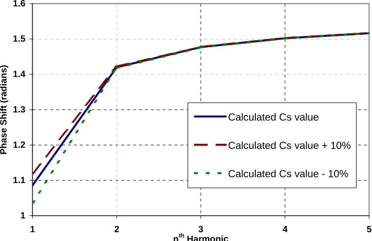
dominates the reactance of the load network. Figure 2.2 represents the phase shift for
different harmonics associated with typical tuned output parameters and the effects of
varying the output capacitor by +/- 10%, as would happen in the second and subsequent
iterations. It is shown that the fundamental frequency is shifted as desired, and the
remainder of the harmonics are virtually unaffected by this variation in capacitance. For
this reason, the iO calculated in the first harmonic will have a and φ remain as variables
for the first harmonic, the magnitude of the additional harmonics will scale linearly with
changes in a, but the phase of the additional harmonics will not be changed by a change
in φ in the next iteration. This way, the second (and subsequent) iterations still have Cp,
conditions and establish convergence on the magnitude of the output current will not
adversely alter the two waveforms that are given as the input conditions to each iteration.
1 1.1 1.2 1.3 1.4 1.5 1.6
1 2 3 4 5
nth Harmonic
P
h
a
s
e
S
h
if
t
(r
a
d
ia
n
s
)
Calculated Cs value
Calculated Cs value + 10%
[image:29.612.116.478.181.416.2]Calculated Cs value - 10%
Figure 2.2 - Phase shift associated with the tuned network and load resistor at the first 5 harmonics. Here, LS = 30nH and CS = 17.8pF for an output phase φ of –0.44 radians at a frequency of 240MHz.
Following this format, the code was written to run for three iterations. It was observed
that the waveforms after the third iteration were nearly identical to those of the second,
and the calculated parameters also had little variation making three iterations adequate for
most situations. In addition to this, the size of the equations grew exponentially as the
iterations progressed due to the symbolic completion of two integrals per iteration
causing an exponential increase in the amount of time needed to complete each iteration.
slight error in the accuracy of the program. This error was negligible except when very
small inductors were given as inputs to the program. This is not an issue using the finite
difference method.
Other limitations of the integral method should also be noted. The transistor is assumed
to turn immediately ON and immediately OFF, with the exception of the exponential
decay in the current when turning OFF. The resistance of the transistor for the vDS
calculation is assumed to go immediately from a constant RON value to an immediate OFF
state without any transition time between the two states. In addition, the resistance of the
inductors due to the low quality factor (Q) on silicon processes has not been accounted
for. Despite these shortcomings, the integral method when published represented the
most concise calculation that the authors had found to date for a Class-E amplifier.
2.2 - Method 2: Finite Difference Method
The finite difference method has many variations and improvements over the integral
method. The most important being that the methodology accepts any gate voltage
waveform as an input to the program (again MATLAB was used), and using this along
with the drain voltage, calculates the resistance of the transistor based on the bias
conditions. The drain current is also defined based on the bias conditions, so the
exponential decay is no longer added as a mathematical term, but is dependant on
transistor parameters given as inputs to the program. The program also accounts for the
intrinsic parasitic resistance of the inductors, thus allowing not only improved accuracy,
technology. Larger inductors using the integral method always provided better results,
but with the finite difference method accounting for the resistance, larger inductors also
mean more loss in the system.
2.2.1 – Defining a Gate Voltage
The finite difference methodology begins with a definition of the gate voltage. The only
stipulations on this are that the waveform must be a function of time (time defined from
zero till the end of one period) and the waveform must be periodic. It is assumed for
most of the simulations that the Class-E amplifier would be driven by a Class-F stage
prior to it. Typically, the output of a Class-F stage consists of two harmonics (first and
third). Although more elaborate tuning networks can be designed, they typically are not
used due to the increased complexity and area with very little increase in performance
[2]. The equations representing a typical Class-F waveform with flattening [2] is
(
)
(
(
)
)
[
17]
21sin t sin 3 t k
k
vGS = ω +θ + ⋅ ω +θ + (2.15)
where k1 is the amplitude of the wave and k2 is the DC offset. These values are typically
set so that the waveform reaches zero volts at its lowest point, and is just under VDD at its
highest. The value of θ will be set by the program to start the waveform at the
appropriate position of the waveform. Since the finite difference method requires initial
conditions, θ will be set so that the waveform begins at a point where conditions of other
waveforms in the circuit are known as seen in Figure 2.1.
As mentioned previously, optimal switching is defined by the condition that the drain
voltage vDS and the parallel capacitor current iCp are both zero when the transistor is just
waveform must be set so that it begins increasing from the threshold voltage of the
transistor (the point where current just starts to flow) at t = 0 as seen in Figure 2.1.
2.2.2 Defining Current Equations from KVL Loop
This technique will still employ an iterative solution to converge on the appropriate
values. Again, the initial assumption of the output current will be defined as
(
ω +φ)
= t
R a
iO sin (2.16)
where all variables are defined the same as they were in the integral method. As before,
a and φ are both variables and will be determined by the program, while the load
resistance R, and radian frequency ω are user defined. Initial guesses are given for a and
φ in the beginning of the program, and the first point in the iLc curve is set equal to the
first point in the iO curve since iCp and iD are both zero at this time as described in the
integral method. The second point in the choke current iLc can then be found using mesh
[image:32.612.228.378.500.650.2]analysis around the loop shown in Figure 2.3.
Figure 2.3 - Loop used with kirchoff’s voltage law in equations 2.17a-e.
+
vLc
-+
vRLc
- +
vDS
-DD Lc
RLc
DS v v V
v + + = (2.17a)
Substituting current expressions into equation 2.16a yields
DD Lc
C Lc Lc
DS V
dt di L R i
v + ⋅ + ⋅ = . (2.17b)
Applying finite difference to the derivative term and quantising the waveforms gives
(
1)
(
1)
Lc( )
Lc(
1)
DS Lc Lc C DD
i n i n
v n i n R L V
t
− −
− + − ⋅ + ⋅ =
∆ . (2.17c)
Separating the difference term and rearranging the equation results in
( )
(
1)
(
)
(
)
1 1
Lc Lc
C C DD DS Lc Lc
i n i n
L L V v n i n R
t t
−
⋅ − ⋅ = − − − − ⋅
∆ ∆ . (2.17d)
And finally, solving for the nth time step from the previous time step yields
( )
(
1)
(
1)
(
1)
Lc Lc DD DS Lc Lc
C
t
i n i n V v n i n R
L
∆
= − + − − − − ⋅ , (2.17e)
where ∆t is the time step between points and RLc is the resistance associated with the
choke inductor LC. To obtain the value of iLc at the second time step of this equation, we
need to know the first point in vDS and iLc. Due to the waveform starting with the
transistor just turning on at t = 0, it is known that vDS(1) = 0 and iLc(1) is equal to iO(1).
2.2.3 Defining Remaining Waveforms from KCL
A similar calculation can be performed to find the drain voltage vDS, except instead of
using Kirchoff’s voltage law to perform mesh analysis, Kirchoff’s current law will be
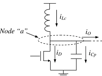
Figure 2.4 - Representation of all currents entering and leaving node “a” in the circuit. Equating the arriving currents to the departing currents will be used in equations 2.18a-e to determine the drain voltage vDS.
Equating the currents entering node “a” and those leaving yields
O D Cp
Lc i i i
i = + + . (2.18a)
Substituting a voltage expression for iCp gives the equation
O D DS p
Lc i i
dt dv C
i = ⋅ + + . (2.18b)
Applying finite difference to the derivative term and quantising the waveforms gives
(
1)
DS( )
DS(
1)
(
1)
(
1)
Lc p D O
v n v n
i n C i n i n
t
− −
− = ⋅ + − + −
∆ . (2.18c)
Separating the difference term and rearranging the equation results in
( )
(
1)
(
)
(
)
(
)
1 1 1
DS DS
p p D O Lc
v n v n
C C i n i n i n
t t
−
⋅ − ⋅ = − + − − −
∆ ∆ . (2.18d)
And finally, solving for the nth time step from the previous time step yields
( )
(
1)
(
1)
(
1)
(
1)
DS DS D O Lc
p
t
v n v n i n i n i n
C
∆
= − + ⋅ − + − − − , (2.18e)
iD iCp
iLc
[image:34.612.213.387.89.218.2]where ∆t is defined as the same time step as in 2.17. It is important to note that an exact
equation for 2.17 and 2.18 would have taken the nth term of each waveform except for the
differential term, which should be split as (n+1/2) and (n-1/2). For ease of calculation,
and since only discrete time steps are taken, the above analysis was used and is valid as
long as a large number of points are used. If the above equations are solved in the above
order, then all required points are available for all time steps except for the drain current
iD, where only the initial condition is know. This waveform must now be defined at each
time step using data already calculated.
2.2.4 – Defining ON Current from Transistor Biasing
Knowing the drain to source voltage vDS and the gate to source voltage vGS, along with the
transistor parameters given as inputs to the program, the bias conditions for the transistor
are known and the current can be calculated. When vGS falls below the threshold voltage
of the transistor VT, the transistor is assumed to be operating in the cut-off region and no
current is assumed. When vGS surpasses VT and vDS is “small” (defined later), the
transistor is assumed to be operating in the linear region, with the current defined as
( )
( )
( )
( )
( )
(LDSEc)
n v DS DS t GS L W ox eff D n v n v n v C n i
V
⋅ ∧ + − ⋅ − ⋅ ⋅ ⋅ ⋅ ⋅ = 1 2 2 2 1 µ, (2.19)
( )
− ⋅
+ =
∧
t GS
eff
V
n v
θ µ µ
1
0 , (2.20)
where θ is defined as ox t
θ β
[23]. Here, tox is the oxide thickness of the transistor and βθ
is given as a typical range of values, and is empirically derived to match the Cadence I-V
curves. Cox in equation 2.18 is the oxide capacitance per unit area, W is the gate width
and L is the gate length of the transistor, and Ec is the critical electric field used to
account for short channel effects present in small gate length transistors [23]. The critical
electric field is approximated as
( )
Vcm cE
=
1
.
7
×
10
4 (2.21)for Si devices [24]. Tsividis however, points out that this parameter is not very easily
modeled, and typically requires fitting from experimental data (Tsividis does not even
present an equation, simply a range of values that should be reasonable) [pp 280-282].
t
V
∧
is used in equation 2.18 as a modification to the standard threshold voltage. It is
known that through Drain Induced Barrier Lowering (DIBL), that the threshold voltage
starts falling below its zero body effect threshold voltage VT0 value in short channel
devices and decreases linearly with vDS [23]. For this case,
V
t∧
will be modeled as
( )
t DS
V v n
t
V
α∧
= − ⋅ (2.22)
The transistor is assumed to remain in the linear region until vDS surpasses the saturation
drain to source voltage VDS’, with VDS’ defined as
( )
( )
c E L t GS t GS DSV
V
n v n v V ⋅ ∧ ∧ ⋅ − + + − ⋅ = 2 1 1 2' . (2.23)
When vDS is greater than VDS’, the transistor is assumed to be in the saturation region,
where the current is assumed to be
( )
( )
( )
+ − + × + ⋅ − ⋅ − ⋅ ⋅ = ⋅ ∧ ' ' 1 1 ' 5 . 0 ' ' 2 DS A DS DS E L V DS DS t GS L W ox eff D V V V n v V V n v C n i c DSV
µ, (2.24)
where VA is the Early voltage of the transistor. The first part of equation 2.24 accounts
for the critical electric field and velocity saturation in short channel MOSFETs while the
second part of the equation is used to account for channel length modulation effects [23].
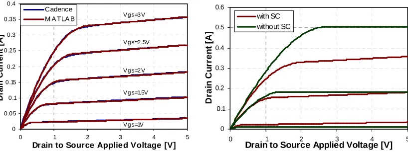
As seen in Figure 2.5, the transistor characteristics much more closely matched the
0 0.05 0.1 0.15 0.2 0.25 0.3 0.35 0.4
0 1 2 3 4 5
Drain to Source Applied Voltage [V]
D ra in C u rr e n t [A ] Cadence
M A TLA B Vgs=3V
Vgs=2.5V Vgs=1.5V Vgs=2V Vgs=1V 0 0.1 0.2 0.3 0.4 0.5 0.6
0 1 2 3 4 5
Drain to Source Applied Voltage [V]
[image:38.612.119.528.95.248.2]D ra in C u rr e n t [A ] with SC without SC
Figure 2.5 – a) Comparison of MATLAB and Cadence I-V curves for a device with a W/L ratio of 1500/0.6 µm. b) Comparison of I-V curves with and without accounting for short channel effects for the same 1500/0.6 µm transistor. Contact resistance was
accounted for in the long channel case.
2.2.5 – Applying Optimal Switching Conditions
At this point in the calculation, all of the waveforms are defined, but the variables Cp, φ,
and a are still unknown. For this methodology, Cp and φ will be adjusted to set vDS and
iCp equal to zero at transistor turn ON, and a will be readjusted based on a comparison of
its assumed value and its calculated value from the Fast Fourier Transform (FFT) of vDS.
The calculation for iO will be the same as it was in the integral method shown in equation
2.12. One modification was made to the iO calculation from the integral method in order
to account for the resistance (RLs) of inductor LS. The new equation accounting for this is
(
)
11 1
sin tan S S
O n DS
n Ls
n L n C
i b n t v
R R ω ω ω − ∞ − = − = ⋅ + ∠ + +
∑
, (2.25)where
( )
(
)
(
(
)
)
1 2
2 1
n n DS Ls S S
b FFT v R R n Lω n Cω
− −
= ⋅ + + −
It was observed that an increase in Cp had the effect of increasing the value of the final
point in the vDS curve while decreasing the value of the final point in iCp. An increase in
the value of φ had the effect of decreasing the end point of both curves. A loop was
established so that the waveforms would be calculated with the initial guesses, the
variables would be adjusted, and the waveforms recalculated. This will continue until the
last point of vDS has a magnitude less than 0.001, iCp is less than 0.0002, and the
difference between a going into the loop and a coming out is less than 0.001. Once this
convergence is set, the output current with five harmonics is calculated and is passed to
the next iteration in the loop. The same criteria was set as in the integral method; the
adjustment of the phase φ will only adjust the phase of the first harmonic, while changes
in the magnitude of a will scale across all harmonics. This method reaches a solution
much faster than the integral method, and 10 or more iterations can be run without taking
too much CPU time. As can be seen in Figure 2.6, the solution typically converges on a
0 0 .5 1 1 .5 2
-2 0 2 4 6 8 1 0 1 2
p i rad ians
D
ra
in
V
o
lt
a
g
e
[image:40.612.189.454.93.286.2]D rain V o ltag e fo r all ite ratio ns (re d is final)
Figure 2.6 – Plot of eight iterations of the drain voltage. As was the case with the integral method, the solution has excellent convergence after three iterations.
2.2.6 – Quantifying Amplifier Performances
At this point, the only thing left to be calculated is the relevant specifications of the
designed amplifier. The output parameters to be considered are THD, efficiency, and
input and output power, as well as the power consumed in the different parts of the
circuit. Since the amplitude of the output current a is known, the output power can be
calculated as
(
)
( )
R
R
I
P
a RMS
out
2 2 2
=
=
. (2.26)Knowing the power supply voltage and the waveform for the power supply current (iLc),
the input power can be defined as the average current times the voltage, 1st
∑
( )
=⋅
=
N n DD Lc inN
V
n
i
P
1. (2.27)
The difference between Pin and Pout represents the power lost in the system, which is a
combination of the power lost in the transistor,
( ) ( )
∑
=⋅
=
N n D DS transN
n
i
n
v
P
1 , (2.28)the power consumed in the inductors,
∑
∑
= =⋅
=
⋅
=
N n Ls O R N n Lc Lc RN
R
i
P
N
R
i
P
Ls Lc 1 1, (2.29)
and the power lost in the unwanted harmonics at the output,
( )
∑
=−
⋅
=
N n out O harmP
N
R
i
P
1 2. (2.30)
From this, the THD can be calculated as the ratio of the power consumed in the
Figure 2.7 – Flow chart for finite difference program. Input user defined circuit
parameters (LC, LS, RLs, RLc, ω, R,
and VDD)and transistor parameters
(W, L, Cox, µn, Ec, Vt, VA)
Define initial approximate values for φ, Cp, a and CS (poor approximations result in more iterations till solution). Define time vector, then iO based on guesses. Define vGS waveform.
Set the vGS waveform so transistor is just turning on at t = 0. Set initial conditions for vDS, iCp, iLc, and iD.
Start of loop of n time steps for one period
Define vDS, iCp, iLc, and iD based on initial values, finite difference, and current and voltage equations
Do vDS, d vDS/dt and iCp = 0 at last point and a out = a in?
Adjust φ, Cp, a, and CS
Redefine iO with harmonics based on filtered vDS waveform.
Start of loop for predefined number of iterations
YES NO
Chapter 3: Results and Discussion
As can be seen from Chapter 2, the modeling of the Class-E amplifier through the use of
MATLAB takes into account a large number of variables and outputs all voltage and
current waveforms, design specifications, and optimized circuit parameters. Due to the
large number of inputs and outputs of the program, the results presented will take into
account the most relevant variables from a design standpoint (inductor sizes, load
resistance, W/L ratio of the transistor, and power supply voltage) and will be limited to
the most pertinent output specifications (output power, efficiency, and Total Harmonic
Distortion [THD]) as well as the optimized circuit components (CP and CS). For
example, the output voltage amplitude a can be obtained from output power for a given
load resistance, and since plots of output power are presented in this chapter, a will not
be. Similarly, the offset phase of the output φ is not as useful of a figure as the capacitor
value (CS) required to produce this phase (only the most pertinent specification will be
presented when much correlation exists between two variables). For all simulations
presented in this chapter, the default parameters will be those of Table 3.1 unless
[image:43.612.232.420.574.697.2]otherwise stated.
Table 3.1 – List of default parameters used in results presented in Chapter 3.
3.1 – Effects of Load Resistance and Transistor Aspect Ratio Variation
Working on a fixed supply system, the biggest influence that the designer has on the
output power would be the load resistance. Considering that the average of the voltage
observed at the drain needs to equal the power supply voltage (minus voltage drop from
the Choke inductor resistance), the vDS waveform will not have much variation in
magnitude with variation in the load resistance. Since the output voltage is simply a
filtered waveform of the drain voltage, the output voltage will not have significant
variation to the changes in load resistance (except for losses in the series inductor LS and
attenuation from the reactance of the slight inductive tuning of the load network). As can
be seen in Figure 3.1, as the load resistor decreases from 100Ω to 20Ω, the power tends
to increase since the voltage is relatively fixed because of an increase in the load current.
However, once the load resistance approaches the ON resistance of the transistor shown
in Figure 3.2 (and that of the resistances of the inductors), the output power drops off
quickly due to the fact that the amplifier is no longer operating near ideal conditions.
Figure 3.2 shows that the ON resistance decreases as the width of the transistor increases.
Note that a total drain and source contact resistance of 1.5Ω was included in the model.
It is interesting to point out that the transistor does not turn immediately ON or OFF as
would happen in the ideal case. This is mostly from the fact that the gate voltage does
not switch instantly, but is modeled as the typical output of a Class-F gate driving stage.
The instantaneous drain voltage of the circuit is also considered in The ON resistance
model is defined as the ratio of the instantaneous drain voltage to the instantaneous drain
0.07 0.09 0.11 0.13 0.15 0.17 0.19
0 10 20 30 40 50 60 70 80 90 100
Load Resistor [ohms]
[image:45.612.198.456.96.226.2]O u tp u t P o w e r [w a tt s ] W=2000 W=1500 W=1000
Figure 3.1 – Variations of output power with load resistance with the transistor width as a parameter. For these plots, RLc=RLs=3Ω.
0 2 4 6 8 1 0 1 2 1 4 1 6 1 8 2 0
0 0 . 2 0 . 4 0 . 6 0 . 8 1
r a d i a n s ( s c a l e d b y p i )
O N r e s is ta n c e [ o h m s ]
W = 1 0 0 0 W = 1 5 0 0 W = 2 0 0 0
0 2 0 4 0 6 0 8 0 1 0 0 1 2 0 1 4 0 1 6 0 1 8 0 2 0 0
0 0 .2 0 . 4 0 . 6 0 . 8 1 1 . 2
r a d i a n s ( s c a l e d b y p i )
O N r e s is ta n c e [ o h m s ]
W = 1 0 0 0 W = 1 5 0 0 W = 2 0 0 0
(a) (b)
Figure 3.2 – (a) ON resistance of the tran