International Journal of Innovative Technology and Exploring Engineering (IJITEE) ISSN: 2278-3075, Volume-8 Issue-8S, June 2019
Abstract: Multipliers can be implemented either in ASIC or FPGA. Comparing FPGAs to ASICs, FPGAs are very flexible. Adding to this, a significant advantage of FPGAs over ASICs is reconfigurability and hardware reusability. FPGA is said to be more advantageous than ASIC multipliers because of its internal optimization algorithms. This research is narrowed down to exploit the advantages of FPGA. Multiplication is a complex process and it is hard to be implemented in hardware environments like ASIC. The process of multiplication consumes more hardware resulting in delay and high power dissipation in ASIC, which is a non-reusable hardware. The complexity in multiplication in ASIC is the problem statement which causes increase in metrics like area, power and delay.
I. INTRODUCTION
Multiplication (Series of repeated additions) is an essential function in basic arithmetic operations, especially in signal processing applications, includes graphics and computation system (Mead, C. and Conway, L., 1988). The factorization of a large number checks whether a number is prime. It depends on multiplication. Multiplicand is the number that is added and the result of it is the product. The number of times that the multiplicand is added is called as the multiplier (Meng, T., 1989). In most of the digital systems such as computers, the bitwidths of the given operands will be the same. Generally, when two operands are multiplied, the outcome has a length which is twice that of the input. The multiplier always saves this information (Miller, R.E., 1965).
Merits of implementation of TP in RCMB: TP technique is used to implement two N/2 operations. It is executed with the same N bit multiplier. N is termed as the bitwidth of the multiplier. Also, as signed multipliers are in common usage, the unsigned TP technique is implemented in signed multipliers like MB and BW. The optimization is done in the TP application in RCMB (Reduced Computation Modified Booth) with less number of MUXes and the results are simulated using Xilinx in FPGA environment. The greatest merit of this proposed work is that by implementing two N/2 multiplications in a single N bit multiplier, double throughput is achieved.
II. LITERATURE REVIEW
Parallel multipliers: M. C. Wen et al., (2005) clarifies a low-power parallel multiplier configuration,
Revised Manuscript Received on May 22, 2019.
Priya Stalin, Associate Professor, Department of ECE, Dr. MGR Educational and Research Institute, Maduravoyal, Chennai95
in which a few sections in the multiplier array can be turned off at whatever point their yields are known. This outline keeps up the original structure without presenting additional limit cells, just like the case in past plans. Trial results demonstrate that it spares 10% of power for random inputs. Higher power reduction can be accomplished if the operands contain the greater number of 0's than 1's.
Truncated multipliers: The work done in Muhammad H. Rais (2010) gives the explanation in the advancement cost for ASICs. This exploration displayed the relative investigation of Spartan-3AN, Virtex-4 and Virtex-5 FPGA devices. The execution of standard and truncated multipliers utilizes Very High Speed Integrated Circuit Hardware Description Language (VHDL). A remarkable decrease in FPGA resources, delay, and power was accomplished utilizing truncated multipliers rather than standard parallel multipliers when the full accuracy of the standard multiplier is not required. The three devices indicated a huge change for truncated multipliers when contrasted with standard multipliers. Results demonstrated that the inconsistency in Spartan-3AN average connection and most extreme pin delay had been proficiently diminished in Virtex-4 and Virtex-5 devices. The Virtex-5 FPGA device demonstrated better execution when contrasted with Spartan-3 and Virtex-4 FPGA devices.
Bypassing Multipliers: The work done in Yin-Tsung Hwang et al.,(2007) concentrates on the column bypassing construct multiplier outlines and focuses on power saving and area. Bypassing is the system utilized as a part of the power saving where a customary Complementary Metal Oxide Semiconductor (CMOS) 28T full adder is received as the base configuration. Other outline choices are likewise investigated. One such is to utilize a 28T full adder design which can be partitioned into two segments, one for the carry logic and the other for the sum logic. The carry logic is an AND-OR-INVERT (AOI) gate took after by an inverter. The complemented carry out signal is likewise bolstered to the sum logic as input. The sum logic is another AOI gate additionally taken after by an inverter. To execute row bypassing plan, two systems are required. Signal multiplexing between the bypassing signal, the assessed signal and evaluation suspension of circumventing full adder. In this paper, C2MOS hardware is received to fill both needs which consolidate the function of logic assessment and transmission gate into one and requires lesser area.
Implementation of Twin Precision-Reduced
Computation Modified Booth Multiplier in
FPGA
(a) Twin Precision-Modified Booth Multiplier: TP is a technique to obtain double output in integer multipliers. With the TP technique, the multipliers adopt to the bitwidth of the operands being computed, which result in reduced power dissipation.
[image:2.595.52.282.174.257.2]By this technique, computational throughput is also increased because many narrow width operations are computed in parallel.
Fig. 1 Signed 8-bit Multiplication using MB Algorithm – An N-bit Multiplication
(M. Sjalander and Per Larsson-Edefors, 2009)
Normally, TP multiplier either performs N bit multiplication or N/2 bit multiplication. The output for a N
bit multiplication is from S0 to S15 as depicted in Fig.1. Fig.1 illustrates the MB multiplication for 8 × 8 which uses recoding logic proposed by Yeh, W.C. and Jen, C. W., (2000). Implementation of TP technique varies for BW and
PLSB0 P10 P40 P30 P20 P50
P60 P80 P70
X7 X6 X5 X4 X3 X2 X1 X0 Y7 Y6 Y5 Y4 Y3 Y2 Y1 Y0
PLSB1 P11 P41 P31 P21 P51
P61 P81 P71
P12
P32 P22 P52
P62
P82 P72 PLSB2
P13
P33 P23 P53
P63
P83 P73 PLSB3
1 0 1 1 aMSP1 aMSP0 1 0 1 1 aLSP1 aLSP0
[image:2.595.322.532.300.560.2]S 0 S 1 S 2 S 3 S 4 S 5 S 6 S 7 S 8 S 9 S 10 S 11 S 12 S 13 S 14 S 15 P42/ PLSB2 P43/ PLSB3 X XOR X X/Y 8 bit/ 4bitoperation
Fig. 2 Implementation of TP in MB Multiplier - N/2Multiplications
(M. Sjalander and Per Larsson-Edefors, 2009)
MB algorithm. Similarly, S0 to S7 and S8 to S15 are the twin outputs for a N/2 bit multiplication, shown in Fig.2.
The outcome of the encoding and decoding logic is the generation of PP array in MB multiplication. Therefore double throughput can be achieved only if changes are accommodated in the recoded N-bit PP array. In MB algorithm the last row in the PP array is meant for an inclusion of sign bit pattern i.e. either 1 or 0. This is due to the negative decoding of MBE. Therefore the number of partial products which has to reduce fromN number of PP rows to N/2 rows becomes [N/2] + 1. In this paper (M. Sjalander and Per Larsson-Edefors, 2009) it is explained that the last row in the PP array is due to 1‟s and 0‟s and ai,
which is caused by precomputation of PLSB. Implementation
in MB multiplication using twin precision technique (M. Sjalander and Per Larsson-Edefors, 2009) is illustrated in Fig.2. It consists of [N/2] + 1 rows and results in a double throughput.
By comparing Fig.1 and Fig.2, the changes needed for the TP implementation of 8 × 8 MB multiplication at each
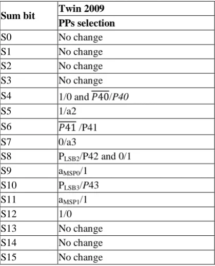
column are tabulated in Table I. The changes between N or N/2 bit multiplication is brought by MUXes. In N-bit multiplication (Fig.1), the S4 column usually has no sign bit. However, a N/2 LSP multiplication requires a sign bit in the same column. Also, there is a need for inversion of MSB bit (P40) in the same place. This is done using MUXes. Similar changes in all the other columns are also done using MUXes.
The following changes are required for the N/2 MSP multiplication: sign bit pattern 1‟s and 0‟s, precomputed LSB (PLSB2, PLSB3) and the potential carry (aMSP0, aMSP1)
which is tabulated in Table I. Totally, for a 16 × 16 TP MB multiplication, nineteen MUXes are needed. For various bitwidths, the MUX utilization is calculated. From the analysis made, for implementation of TP in MB (M. Sjalander and Per Larsson-Edefors, 2009), it is clear that this method inquires (bitwidth+ 3) MUXes.
Table. 1 Changes needed for Twin Precision in a N bit MB Multiplier
Sum bit Twin 2009 PPs selection
S0 No change
S1 No change
S2 No change
S3 No change
S4 1/0 and 𝑃40/P40
S5 1/a2
S6 𝑃41 /P41
S7 0/a3
S8 PLSB2/P42 and 0/1
S9 aMSP0/1
S10 PLSB3/P43
S11 aMSP1/1
S12 1/0
S13 No change S14 No change S15 No change
TP implementation to signed multipliers is made in (M.Sjalander and Per Larsson-Edefors, 2009) and further optimization in TP multiplier is not done.There is a generation of [N/2] +1 PP rows in TP implementation; it adopts sign extension scheme presented in (J. Ardekani, 1993). TP implementation in MB (J. Fadavi-Ardekani, 1993) requires that more changes are to be made for N/2 bit multiplication as it adopts a sign extension scheme. As many the changes, in a N/2 bit multiplication that much is the need for MUXes. They are deployed to select required PPs for N and N/2 bit multiplications.
For twin precision implementation in MB algorithm (M. Själander and Per Larsson-Edefors, 2009), Booth encoding and decoding is required. Then inclusion of PLSB is done.
PLSB0
P10
P40 P30 P20
P50
P60 P80 P70
Y7 Y6 Y5 Y4 Y3 Y2 Y1 Y0
PLSB1
P11
P41 P31 P21
P51
P61
P81
P71
P12
P42 P32 P22
P52
P62
P82 P72 PLSB2
P13
P43 P33 P23
P53
P63
P83 P73 PLSB3
1 0 1 0 1 1 1 a1 a0
S0 S1 S2 S3 S4 S5 S6 S7 S8 S9 S 10 S 11 S 12 S 13 S 14
0 a3 a2
X7 X6 X5 X4 X3 X2 X1 X0
[image:2.595.52.276.388.520.2]International Journal of Innovative Technology and Exploring Engineering (IJITEE) ISSN: 2278-3075, Volume-8 Issue-8S, June 2019
Along with this, there is a need for potential carry (aMSP).
These steps are done distinctly for both N/2 LSP and MSP multiplications. And also sign extension has to be made separately for the two N/2 bit multiplications. In RCMB (FabrizioLamberti et al., 2011), the following steps are performed for a N/2 bit multiplication:
(i) Booth encoding and decoding, (ii) neg bit is added in the LSB of each PP row for two‟s complement representation, (iii) 1‟s are added for sign extension. There is no requirement for the inclusion of PLSB and
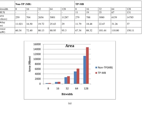
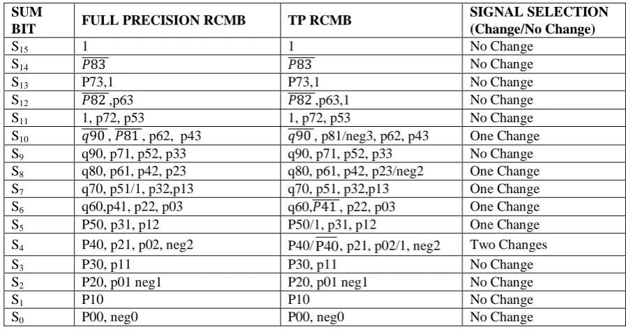
potential carry in RCMB. This reduces the complexity of the system. So this makes it suitable for TP implementation and therefore, utilization of MUXes gets reduced. For an 8 × 8 TP multiplier, twin 2009 (M. Sjalander and Per Larsson-Edefors, 2009) requires eleven MUXes. Similarly for the implementation of a 16 × 16 TP multiplier, nineteen MUXes are required which is tabulated in Table II. Therefore the total MUX requirement for TP implementation in MB is formulated as N+3. Also, it gives the simulated results of MB and TP-MB using Xilinx software. Fig.3 (a), (b) & (c) illustrates the changes in the area, power, and delay in the implementation of TP in MB multiplier.
TP-MB in ASIC environment was given (M. Sjalander and Per Larsson-Edefors, 2009), whereas Table II gives the same in FPGA environment. This is done for evaluating the performance of the same with TP-RCMB in FPGA. Normally to achieve double throughput (twin output), N bit and N/2 bit multipliers are required. However, by implementing TP technique, the same double throughput is achieved not at the cost of twice the area required for N bit and N/2 bit multiplications but with a slight increase in area of 7.2% to 23.7%, an increase in delay of 6.5% to 21.6 % and an increase in power of 10% to 36.5 % for varying bit widths of N=8 to 128 bits, which is graphically represented in Fig. 3. This is due to the MUX requirement and the logic incorporated to make the unwanted PPs to zero.
[image:3.595.61.546.347.736.2]Double throughput in FPGA environment is achieved effectively by implementing TP technique in MB. This chapter also explains the different kinds of MB encoders and decoders. Also, mapping of the PPs to an HPM tree is described in this chapter. This implementation requires less changes in the PP array to acquire TP. Selection of appropriate PPs for N or N/2 bit multiplication is satisfied by the MUX utilization. The discussion of implementation of TP-MB formulates the MUX requirement as N+3.
Table. 2 Simulated Results of MB and TP-MB using Xilinx
Non-TP (MB) TP-MB
Bitwidth 8 16 32 64 128 8 16 32 64 128
MUX - - - 11 19 35 67 131
Area
(slices) 259 704 2656 5001 11287 279 788 3080 6159 14785 Delay
(ns) 11.021 16.50 19.72 25.63 29 11.79 18.48 22.67 31.26 37 Power
(mW) 60.34 72.40 80.13 88.95 95.3 67.34 88.32 101.44 110.80 150.11
(a) 0
2000 4000 6000 8000 10000 12000 14000 16000
8 16 32 64 128
A
r
e
a
(S
li
c
e
s)
Bitwidth
Area
Non-TP(MB)
(b)
(c)
Fig. 3 (a) Bitwidth vs Area (b) Bitwidthvs Delay (c) Bitwidthvs Power Twin Precision Reduced Computation Modified Booth
Multiplier in FPGA:
Here the performance of a RCMB multiplier with TP technique implemented in FPGA is explained. The multiplier results in double throughput. TP technique is an efficient way to obtain double throughput in the multipliers. The idea of implementing the TP technique to RCMB is done in ASIC (Asirvatham.R. and Ramachandran.S., 2015) environment. The optimization is done by reducing the MUX utilization. But in the case of ASIC, the power consumption increases per unit die size than that in FPGA. Therefore, if optimization is done in FPGA, it is an added advantage.
Algorithm for obtaining TP in RCMB
1. MRC{p,q } - Matrix set with reduced complexity
𝑝 = 1 𝑡𝑜N
2 ; 𝑞 = 1 𝑡𝑜 2N;
N = Bitwidth; MRC consists of equal number of bits in each
row.
2. For N = 8, upper limit = UL{ p1, p2 }; lower limit = LL{ p3,
p4 }
3. (PPp,q∈ (p,q)); Partial product is an element of p and q
4. TB = N + 3; TB =total number of bits per row.
5. Negation and inclusion of sign bit 1s are needed for TP (i) Negation of bit MSB is done necessarily. It is achieved by performing N/2 LSB multiplication which is given as
BT[Lp]. Lp value gives relative bit position in the pth row so that negation of MSB can be made correctly.
for
𝑝 = 1 ; L = 𝐿𝑝= T𝐵− UN
𝑝 = 2 toN
4 ; L = L𝑝= L 𝑝−1 + 2
(1)
BT[Lp] - Bit (BT) position (L) in the corresponding p row
U𝑁=
N
2+ 2 (2)
UN – Unchanging value based on N
(ii-a) Inclusion of 1s in subsequent columns (q) are made for following iterations
Iteration (I) = 1 to (N/4) + 1
for
I = 1 quo I = quo 1 =
𝑁
2 + 1
I = 2 quo I = quo 2 =
𝑁
2 + 2
I = 3 to 𝑁 4 + 1 quo I = quo I−1 + 2
(3) 0
5 10 15 20 25 30 35 40
8 16 32 64 128
D
e
lay
(n
s)
Bitwidth
Delay
Non-TP(MB)
TP-MB
0 20 40 60 80 100 120 140 160
8 16 32 64 128
P
o
w
er
(m
W)
Bitwidth
Power
Non-TP(MB)
[image:4.595.136.461.46.464.2]International Journal of Innovative Technology and Exploring Engineering (IJITEE) ISSN: 2278-3075, Volume-8 Issue-8S, June 2019
quo(I) denotes the upper (U) limit in the corresponding
column (q) and the ones (O) in it for corresponding iteration (I).
(ii-b)
OLL 𝑞 =
𝑁
2+ 1 + 𝑁 (4)
OLL(q) denotes the inclusion of 1s in the lower limit in the corresponding column q.
6. Negative bits (negk) are included in the LSB postion of each PP row for N/2 MSP multiplication. For this, the column (q) on row (p) is to be known. The variation of k
is from 0 to (N/2 − 1).
negk → 𝑞 𝑝
for
𝑝 =𝑁 4+ 1 , k =
𝑁
4 , 𝑞 𝑝 = 𝑁 + 1 𝑝 = 𝑁
4+ 2 to N/2 , k = 𝑁 4+ 1 to
𝑁
2− 1 , 𝑞 𝑝 = 𝑞 𝑝−1 + 2
(5) p = row, q = column
TB = 𝑁 + 3 6
TB denotes the number of bits in a row.
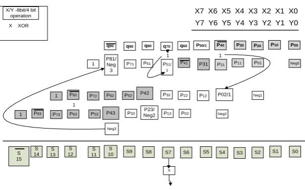
For an 8 × 8 RCMB multiplier illustrated in Fig. 4, TB = 11 and this is constantly the same for all the rows. When N/2 LSP multiplication is performed, the most significant bit in each PP row has to be negated. The bit position (Lp) in the upper limit is given as BT[Lp], given in Equation (1). It is to be known for the inversion step to be processed and BT is the bit and Lp denotes the bit position in the corresponding row (p). The inversion of bits is carried out during an N-bit multiplication. That itself is sufficient for the lower limit N/2 MSP multiplication. The bits are negated on the upper limit and it is described in Equation (1).
For rows p = 1 to N/4, the inversion of bits BT[Lp] is done. For initial conditions p = 1, [Lp] is the difference between total bits TB(p) in a single row and the unchanging value UN.
BT[Lp] denotes the position of the bit in the subsequent pth row.
UNis the unchanging value which is based on N value. For N = 16, the inversion of the eleventh, thirteenth and fifteenth bits is required. For N = 8, the values of 𝐿1 = 5 and
𝐿2 = 7. Hence, the inversion of the fifth and seventh bits is
done in the upper limit as shown in Fig.4.
For the lower part of the twin multiplication to be done, some changes are made in the upper limit and some in the lower limit for the other part of the twin implementation. For a 2's complement representation, sign extension scheme includes 1s in the suitable column. More changes are required in upper limit. So in this algorithm for obtaining TP, an inclusion of 1s for a 2‟s complement representation in corresponding column (q) is performed in the upper limit according to Equation (3).
The implementation of TP in RCMB gives better performance compared to the existing Twin (M. Sjalander and Per Larsson-Edefors, 2009) and TP-RCMB implementation in ASIC environment (Asirvatham R. and Ramachandran S., 2015). This implementation yields less MUX utilization. The hardware complexity, latency and power calculation is analyzed. In the existing work, changes made for N and N/2 bit multiplications are selected using MUXes, which increase the design complexity of the multiplier. But the same is reduced in TP-RCMB in FPGA. One significant reason is the reduction of PP row height. Other reasons are certainly the optimizations provided by the FPGA.
The sign extension in a 2‟s complement representation is prevented by the addition of sign bit pattern 1‟s and 0‟s. This varies for N and N/2 bit multiplication. Bit position is significant for particular column p; otherwise the sum bit becomes erroneous. But ruling out the particular column q is sufficient in adding 1‟s. Therefore, it is not necessary to rule out the bit position. quo(I) denotes the upper (U) limit in the
corresponding column (q) and the ones (O) in it for corresponding iteration (I)
Y7 Y6 Y5 Y4 Y3 Y2 Y1 Y0 X7 X6 X5 X4 X3 X2 X1 X0 X/Y -8bit/4 bit
operation X XOR
P00 P10 P40 P30 P20 P50/1
q60 q90 q80 q70 q90
P01
P11
P41 P31 P21
P51/ 1
P61
1 P71 Neg0
P02/1 P12
P42 P32 P22
P52
P62
1 P82 P72 Neg1
P03
P13
P33
P53
P63
1 P83 P73 Neg2
1
S0 S1 S2 S3 S4 S5 S6 S7 S8 S9 S 10 S 11 S 12 S 13 S 14 S 15
1
P23/ Neg2 P81/
Neg 3
X
P43
1
[image:5.595.145.453.512.703.2]Neg3
Fig. 4 Implementation of TP-RCMB to Obtain Twin Output So in the ninth, tenth and twelveth and fourteenth
width plus one. A „1' is added in the columns N
2 + 1
and N2 + 2 for iteration I=1 and 2. The consecutive values
of I is the total of previous iteration value and a two. In Fig.4, the „1‟ that is inserted in the fifth column is joined with PP, P02 and is represented as P02/1 for a Full/Twin in the Least Significant Part. MUXes are used for selection between signals.
A combination of P50 and 1 is put up in the 6th column. To prevent the N/2 MSP multiplication from the carry of the previous LSP multiplication affecting the second half, a „1‟ is inserted in the eighth column which passes through a XOR gate. Hence the S(N-1) gets negated. A „1‟ is added in the 13th column in the lower limit for the TP implementation as per Equation (4) for a value of N=8. It is not necessary to put extra effort to insert 1s in the lower limit for N/2 MSP multiplication. The sign bits allotted for a full precision multiplication of RCMB can be very well used.
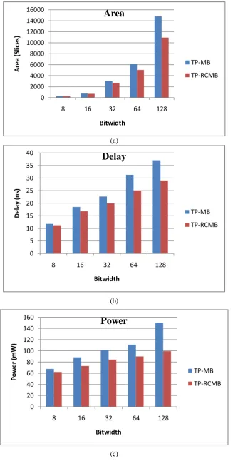
[image:6.595.72.521.296.532.2]The 8 × 8 RCMB multiplier is chosen to explain the proposed idea. From the consolidated changes, it is revealed that [N/2]+3MUXes are entailed for TP-RCMB and verified for various bitwidths, as charted in Table III. Nearly 41% to 47% (for N = 8 to 128) of less MUXesis utilized compared to the previous work (M. Sjalander and Per Larsson-Edefors, 2009).The concept of optimization is not done (M. Sjalander and Per Larsson-Edefors, 2009) in TP implementation. Though the work of TP optimization is extended to signed multipliers in ASIC environment (Asirvatham R. and Ramachandran S., 2015), the parameters influencing the design are less appreciable. Compared to the prior work (M. Sjalander and Per Larsson-Edefors, 2009), the method of implementation requires fewer changes for performing aN/2 operation. These changes inPPs are typically selected using MUXes. The proposed TP in RCMB method decreases the area and delay as the design and project cycle in FPGA are smaller than those in ASIC.
Table. 3 Changes to be made to Implement TP in RCMB SUM
BIT FULL PRECISION RCMB TP RCMB
SIGNAL SELECTION (Change/No Change)
S15 1 1 No Change
S14 𝑃83 𝑃83 No Change
S13 P73,1 P73,1 No Change
S12 𝑃82 ,p63 𝑃82 ,p63,1 No Change
S11 1, p72, p53 1, p72, p53 No Change
S10 𝑞90 , 𝑃81 , p62, p43 𝑞90 , p81/neg3, p62, p43 One Change
S9 q90, p71, p52, p33 q90, p71, p52, p33 No Change
S8 q80, p61, p42, p23 q80, p61, p42, p23/neg2 One Change
S7 q70, p51/1, p32,p13 q70, p51, p32,p13 One Change
S6 q60,p41, p22, p03 q60,𝑃41 , p22, p03 One Change
S5 P50, p31, p12 P50/1, p31, p12 One Change
S4 P40, p21, p02, neg2 P40/ P40, p21, p02/1, neg2 Two Changes
S3 P30, p11 P30, p11 No Change
S2 P20, p01 neg1 P20, p01 neg1 No Change
S1 P10 P10 No Change
S0 P00, neg0 P00, neg0 No Change
From Table IV, it is inferred that the TP implementation in RCMB achieves a reduction in delay of about 5% to 22%, area ranges from 5% to26% and the power reduction is from8%to 34% in FPGA environment. This is more appreciable compared to 5% to 20% reduction in delay, 5% to 18% of the reduction in area and a power reduction of 8% to 32% in ASIC (Asirvatham R. and Ramachandran S., 2015) environment. It is due to the following reasons. (i) In Xilinx FPGAs, a CLB has been any divided into many slices. A slice in most of the Xilinx devices consists
of2LUTs and two flip-flops. There is additionally a special logic in the slice which changes the usually performed operations like combining two LUTs into a bigger LUT and making economical adders. (ii) To improve the performance of arithmetic operations, the special connections obtainable that permits LUT to operate as an economical full adder (Andreas Ehliar, 2009).This can be noted as a carry chain. It is additionally connected to adjacent slices to permit for larger adders to be created.
Table. 4 Comparison of TP-MB and TP-RCMB using Xilinx
TP-MB TP-RCMB
Bitwidth 8 16 32 64 128 8 16 32 64 128
Mux 11 19 35 67 131 7 11 19 35 67
International Journal of Innovative Technology and Exploring Engineering (IJITEE) ISSN: 2278-3075, Volume-8 Issue-8S, June 2019
Fig. 4 is a typical representation of area, power and delay tabulated in Table III. It gives the performance evaluation of TP in MB by M. Sjalander and Per Larsson-Edefors, 2009
and TP implementation in RCMB. Illustration of area, delay and power for TP-MB and the proposed TP-RCMB in FPGA is depicted in Fig. 4 (a), (b) & (c).
(a)
(b)
(c)
Fig. 4 (a) Bitwidth Vs Area (b) Bitwidth Vs Delay (c) Bitwidth Vs Power 0
2000 4000 6000 8000 10000 12000 14000 16000
8 16 32 64 128
A
rea
(Sl
ic
es
)
Bitwidth
Area
TP-MB
TP-RCMB
0 5 10 15 20 25 30 35 40
8 16 32 64 128
D
e
la
y
(n
s)
Bitwidth
Delay
TP-MB
TP-RCMB
0 20 40 60 80 100 120 140 160
8 16 32 64 128
P
o
w
er
(m
W)
Bitwidth
Power
TP-MB
III. CONCLUSION
Double throughput is achieved effectively by implementing TP technique in RCMB in the FPGA environment. The proposed approach of implementation requires fewer changes in the PP array to acquire TP. As per the multiplication requirement, i.e. for an N or N/2 bit operation, MUXes do the selection of specific PPs in TP multiplier. The overall delay, area and power get reduced when the results are compared with TP-RCMB in an ASIC environment.
REFERENCES
1. Abdelgawad, A., and Bayoumi, M., "High Speed and Area-Efficient Multiply Accumulate (MAC) Unit for Digital Signal Prossing Applications", IEEE International Symposium on Circuits and Systems, pp. 3199-3202, 2007.
2. About ASIC & FPGA. http://www.altera.com
3. Albert, D. and Dimitri, T., “Architecture and Implementation of a Vector /SIMD Multiply-Accumulate Unit”, IEEE Trans. on Computers, Vol.54, No.3, pp.284-293, 2005.
4. Altera DE1 Board. http://www.terasic.com.tw/cgi-bin/page/archive.pl? No=83.
5. Amaricai, A., Vladutiu, M. and Boncalo, O.,"Design Issues and Implementations for Floating-Point Divide-Add Fused", IEEE Trans. Circuits Syst. II–Exp. Briefs, Vol. 57, No. 4, pp. 295-299, 2010. 6. Amora, A.D., Nannarelli , A., Re,M. and Cardarilli, G.C.," Reducing
Power Dissipation in Complex Digital Filters by using the Quadratic Residue Number System", Proc. of 34th Asilomar Conference on Signals, Systems and Computers, pp. 879-883, 2000.
7. Anitha,R., Alekhya, N., Jesima,L. W. and Bagyaveereswaran,V.,
"Comparative Study of High Performance Braun's Multiplier using
FPGAs", IOSR Journal of Electronics and Communication
Engineering, Vol. 1, No. 4, pp. 33-37, 2012.
8. Ardekani, J.F., "MxN Booth Encoded Multiplier Generator Using Optimized Wallace Trees", Proceedings IEEE International Conference on Computer Design: VLSI in Computers and Processors, ICCD '92, pp.1-4, 1992.
9. Ashour, M.A. and Saleh, H.I., "An FPGA implementation guide for some different types of Serial - Parallel Multiplier Structures", Microelectronics Journal, Vol.31, No.3, pp.161-168, 2000.
10.Asirvatham, R. and Ramachandran, S., "An Optimised Twin Precision Multiplier for ASIC Environment", EURASIP Journal on Advances in Signal Processing, pp. 1-18, 2015.
11.Bala, P.S. and Raghavendra, S., "A New VLSI Architecture of Parallel Multiplier - Accumulator Based on Radix-2 Modified Booth Algorithm",IEEE Trans. on Very Large Scale Integration (VLSI) Systems, Vol.18, No. 2, pp. 91–97, 2011.
12.Baugh, C. R. and Wooley, B. A., “A Two‟s Complement Parallel Array
Multiplication Algorithm” , IEEE Trans. Computers, Vol. 22, No. 12, pp. 1045-1047, 1973.
13.Bhardwaj, M., Min, R. and Chandrakasan, A.P., "Quantifying and Enhancing Power Awareness of VLSI Systems", IEEE Trans. on Very Large Scale Integration (VLSI) Systems, Vol. 9, No. 6, pp.757–772, 2001.
14.Booth, A.D., "A signed binary multiplication technique", The Quarterly Journal of Mechanics and Applied Mathematics Vol. 4, No. 2, pp. 236-240, 1950.
15.Brooks, D. and Martonosi, M., "Dynamically Exploiting Narrow Width Operands to Improve Processor Power and Performance", IEEE Proceedings Fifth International Symposium on High-Performance Computer Architecture, pp. 13 - 22, 1999.