International Journal of Innovative Technology and Exploring Engineering (IJITEE) ISSN: 2278-3075, Volume-8 Issue-10, August 2019
Abstract: In recent time, various lightweight algorithms have been proposed to provide security in a constrained resource environment. With so many algorithms and their different implementations, it is hard to choose the appropriate security primitive for an application. In this work, various hardware implementations of lightweight block cipher RECTANGLE is proposed like Iterative design, 16-bits architecture, Reduced Substitution box design, RAM-based design and Iterative design with Partial loop unrolled. These designs provide aid in overcoming the problem of security in a constrained resource environment. Architectures are designed and implemented in various FPGA platforms. Results are extensively evaluated and compared on the basis of throughput, throughput/slice, area utilization, energy requirement and power consumption for their implementation in different FPGA platforms. Best trade-off among throughput and area is given by Iterative design with partial loop unrolling. It also gave best energy consumption values for all FPGAs. Ram-based design utilized least number of registers for its implementation.
Keywords: BRAM, FPGA, lightweight cryptography, Security, RECTANGLE Cipher, Hardware architecture.
I. INTRODUCTION
With the advancement in technology, there is a huge development in various ubiquitous computing devices like smart cards, Radio- frequency Identification tags (RFID), smartphones etc. Ubiquitous computing among various devices puts a major effect in real life environment [1]. With the growing use of these devices and rapid growth of Internet of things (IoT), there is a constant threat to security and privacy of the information. These small devices are equipped with slow oscillators and low-end microcontrollers, which have small word length [2]. There are also limited power generation resources available. As a result, performance enhancement is achieved by using various power optimization techniques [3], novel transmission techniques [4] or by using energy harvesting technique [5]. One of the widely used techniques to safeguard data is by using Data Encryption [6]. Many ciphers are introduced to combat the issue of security and privacy. For example, some traditional ciphers like advanced encryption standards (AES)
Revised Manuscript Received on August 10, 2019. * Correspondence Author
Nivedita Shrivastava, Department of Electronics & Communication Engineering, National Institute of Technology Raipur, Raipur-492010, Chhattisgarh India. Email: [email protected]
Bibhudendra Acharya*, Department of Electronics & Communication Engineering, National Institute of Technology, Raipur, Raipur-492010, Chhattisgarh India. Email: [email protected]
[7] and Data encryption standard (DES) [8] are proposed. In the field of lightweight cryptography also many ciphers are introduced in order to deal with security concerns in the field of constrained resource environment. Lightweight ciphers are mainly divided as Substitution-permutation network (SPN) based ciphers and Feistel network based ciphers. In SPN based ciphers confusion and diffusion of bits is performed. Some of the popular SPN based ciphers are PRESENT [9], RECTANGLE [10], KLEIN [11], Light encryption device (LED) [12], mCrypton [13] etc. Another category of lightweight ciphers is Feistel cipher. In these ciphers encryption is performed on half of the data, thus they require more number of rounds in order to provide proper security. Some of the famous Feistel ciphers are CLEFIA [14], SIMON and SPECK [15], PICCOLO [16], TWINE [17], LBLOCK [18] etc. To make our day-to-day life simpler, IoT is inherently applied in all domains [19]. Security, performance, and availability are the major challenges, which are observed in the IoT environment [20]. For IoT based applications, hardware-based solutions are considered ideal in order to provide security [21]. Various optimization techniques are proposed by several authors. With optimization, these ciphers become more suitable for resource scare lightweight applications. Lightweight algorithms have been implemented in application specific integrated circuits (ASIC). Due to feature of non-recurring engineering (NRE), implementation cost in ASIC is very high and they also require long manufacturing time, that makes ASICs undesirable for low volume products. For the production of the devices like RFIDs, sensor nodes etc., low-cost and low-power Field programmable gate array (FPGA) [22] are preferred, as they possess low or zero NRE cost along with reconfigurable nature with reduced time to market [23]. Reconfigurable nature of FPGA allows easy upgrades at low cost [24]. Also with the usage of FPGA, we can reduce hardware resources [25]. As the nature of security protocols are rapidly evolving, there is a need for reconfigurable devices [26]. Another advantage of FPGA is in-built Block Random access memory (BRAM) [27]. In random access memory (RAM) based architecture BRAM is utilized for implementation of hardware architecture, leaving registers free to be used for any other purpose.
A. Contribution
In the proposed work different hardware architecture of RECTANGLE block cipher is proposed for FPGA implementation. These architectures have different resource and power consumption. According to the requirement, these architectures can be used by users. The main contribution of the paper is as follows:
FPGA Implementation of RECTANGLE Block
Cipher Architectures
Iterative Architecture for both 80-bits and 128-bits key schedule along with a finite state machine (FSM), which is used to control the circuit. Reduced S-box architecture with 80-bits key generation mechanism is also proposed.
16-bits architecture with key scheduling of both 80-bits and 128-bits key length are proposed. These architectures have a reduction in datapath width from 64-bits to 16-bits.
Two RAM based designs are proposed which aims in reducing area consumption of the architecture. In this architecture, BRAM of FPGA is used for storing an intermediate state of the design. In the first work, S-box is implemented using slices available in FPGA. In other design S-box in implemented in BRAM itself.
Iterative design with partial Loop Unrolling is proposed. Five rounds of RECTANGLE cipher are unrolled and connected serially with each other. ROM based key retrieval mechanism is used.
Evaluation of different works is done on the basis of area requirement, power consumption, energy requirement, latency, throughput, and throughput/slice. Evaluation of all the architectures is done in four different FPGA platforms.
B. Organization of paper
The paper is divided into six sections. Section 2 comprises of basic description of RECTANGLE cipher algorithm. Section 3 describes the proposed hardware architectures of the RECTANGLE block cipher for FPGA implementation. Section 4 comprises of metrics and methodology used for performing the work. Section 5 illustrates results obtained for different designs. It also includes discussion, evaluation and comparison of the obtained results. Finally, Section 6 presents the final conclusion.
II. THERECTANGLECIPHER:ALGORITHM The RECTANGLE block cipher is a hardware-friendly lightweight cipher. This is an SPN based cipher and comprises of 25 rounds of encryption. This cipher can work with the key schedule of both 80-bits and 128-bits. Selection of key schedule depends on the requirement of user i.e. whether high security or less resource consumption is desired. Cipher architecture consists of data scheduling and key scheduling part. Data scheduling part consists of three basic operations, which are performed in each round of encryption. These operations are described as follow:
AddRoundKey Operation: Simple XOR operation
between 64-bits of round subkey and intermediate data is performed during the encryption process.
Substitution Layer: This operation performs substitution
of 64-bits, through a set of 16 Boolean S-boxes. S-box accepts input of 4-bits and produces output of 4-bits. There are various methods available to design S-box like Boolean logic based S-box, RAM-based S-box, look-up table (LUT) based S-box etc.
Permutation Layer: This layer performs permutation in
64-bits of data. Data is divided in the set of 16-bits, and rotation is performed in each bit set. In each of the
16-bits, rotation offset of 0, 1, 12, and 13 is used respectively.
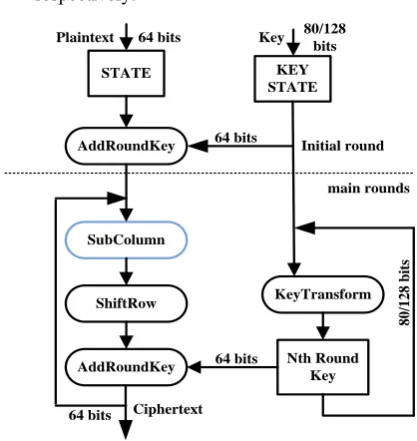
Plaintext
STATE
AddRoundKey
SubColumn
ShiftRow
AddRoundKey
KeyTransform
Nth Round Key KEY STATE
64 bits
64 bits
main rounds 80/128
bits
64 bits
8
0
/1
2
8
b
it
s
Key
Ciphertext 64 bits
[image:2.595.316.525.72.293.2]Initial round
Fig. 1. Encryption Process of RECTANGLE cipher. Plaintext is encrypted through various rounds of encryption and round subkey is generated simultaneously through the key scheduling part
In Fig. 1, the basic algorithm of RECTANGLE is shown. The ciphertext is achieved after completion of all the rounds and an additional AddRoundKey operation. For each round, a subkey is generated using key scheduling mechanism. This mechanism comprises of substitution operation followed by generalized Feistel transformation. Thereafter, XOR operation with round constant is performed. It is generated through a linear feedback shift register (LFSR) of 5-bits.
III. HARDWAREARCHITECTUREOF
RECTANGLEBLOCKCIPHER
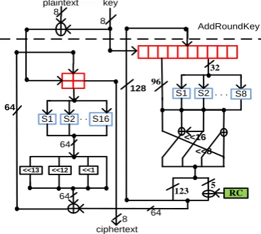
A. Reduced S-Box Architecture
RECTANGLE cipher has a block size of 64-bits. For storing data and key, 64-bits and 80-bits registers are used respectively. Authors used 16 S-boxes to design the substitution layer of the RECTANGLE cipher [10]. In the proposed architecture, number of S-boxes in the data scheduling part is reduced from 16 to just two.
It is observed that S-boxes and registers require maximum area for their implementation. Reduction in the number of S-boxes results in the reduction of area. But there are two disadvantages of this architecture. First is to process 64-bits, 8 extra clock cycles are required. This results in increase of latency. Another disadvantage is as the datapath width is varied, so extra circuitry is required to synchronize the design. As a result, there is an introduction of extra area overhead. Two clock cycles are required to take the input and to process the output. For processing all rounds, 192 clock cycles are required. This leads to latency of 194 clock cycles. This architecture requires 149
International Journal of Innovative Technology and Exploring Engineering (IJITEE) ISSN: 2278-3075, Volume-8 Issue-10, August 2019
S1 S2
P-Layer
key
96
32
123 5
RC 4
64
64
4
8 64 64
128
64
<<16
<<8 S-Box Layer
128
C
ip
h
er
te
[image:3.595.375.495.53.133.2]xt
Fig. 2. Hardware Architecture of RECTANGLE block cipher. The main characteristic of this design is the reduced number of S-boxes
B. Iterative Architecture
In this architecture, 8-bits I/O ports are used for data and key. For storing data, a 64-bits register is used while for key 80-bits register is used. As shown in Fig. 3, 8-bits XOR gate is used to perform initial AddRoundKey operation. As it uses a key size of 128-bits, this architecture is preferred when there is a need for higher security.
For synchronizing and controlling the circuit FSM is used, which is shown in Fig. 4. As the circuit is reset, it enters in initial ‘BOOT’ state. Then directly goes to ‘IDLE’ state. When the user gives ‘en’ signal data loading begins. For the first eight cycles, both data and key register are loaded and FSM stays in ‘LD0’ state. As the counter reaches count of seven, it gets reset and FSM reaches ‘LD1’ state. Key is loaded in the key register for the next eight clock cycles. When the counter reaches seven, loading is completed. The counter resets again and FSM reaches ‘ENC’ state. In this state in a single clock cycle, one round of encryption is performed. After completion of all the rounds, data is unloaded in ‘ULD’ state for the next 8 cycles. At last FSM reaches ‘BOOT’ state and the device is ready to be used again.
64
8 8
8
64
128
ciphertext
plaintext key
96
32
123 5 RC
<<16
<<8
S1 S2. . S16
64
64
S1 S2 . . . S8
<<12
<<13 <<1
[image:3.595.76.269.62.229.2]AddRoundKey
Fig. 3. Iterative Architecture of RECTANGLE block cipher with 128-bits key Schedule. This architecture closely follows the basic specification of RECTANGLE cipher with 128-bits key schedule
BOOT LD0
LD1
Co
un
t=
7
Co
un
t=
7
en=0
Co
unt=!7
Co un t= 7
IDLE en=1
Co
un
t=
!7
Co un t= 7
ULD
ENC
[image:3.595.382.478.536.614.2]rst
Fig. 4. Six stages finite state machine for Iterative Architecture of RECTANGLE block cipher with 128-bits key Schedule. FSM generates required control signals to control the working of circuitry
For the design with 80-bits key schedule, FSM is same as 128-bits architecture. The only difference is change from ‘LD1’ to ‘ENC’ state happens when the counter reaches 2. 8 cycles are required to store data and two extra cycles are required to store the key. 8 clock-cycles are required for generating output. So latency of the architecture comes out to be 42. In this work 149 flop-flops, 20 Boolean S-box and one Permutation layer (P-layer) is used.
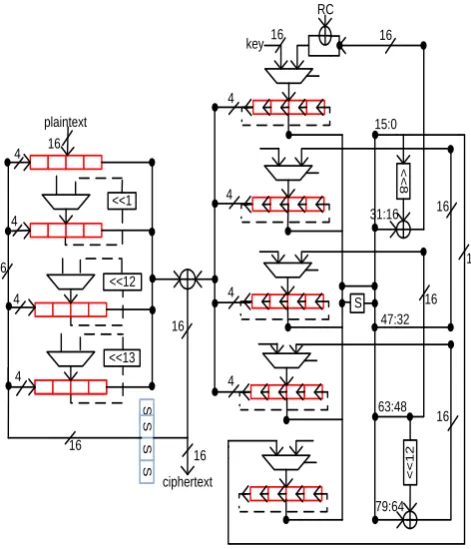
C. 16-bits Architecture with Key Scheduling
In this work, I/O port of 16-bits is used. Datapath width of the architecture is reduced from 64 to 16-bits. Conventionally to optimize architecture, datapath width is varied. This requires large area overhead, as to transfer data from small to a wider word or vice versa requires extra registers for storing data, which leads to the increased area [28].
For data scheduling part, four 16-bits shift registers are required to store the plaintext. These registers are designed to provide serial and parallel, input-output operations. The idea for implementing registers with both shift and parallel access is taken from work done in [29]. Another feature of this design is the reduction in the number of S-boxes from 20 to just 8. Permutation is performed with the help of parallel operation of the 16-bits shift register. So no extra P-layer is needed to perform diffusion of bits. Architecture is designed for the key schedule of both 80-bits and 128-bits key length. Fig. 6 and Fig. 7 shows the architecture of the same.
IDLE
ENC
LD0
LD1 En=1
C
o
u
nt
=
3
C
o
u
nt
=
10
4
Count=1
Fig. 5. Finite State Machine for 16-bits architecture with 80-bits key Scheduling. This FSM generates control signals for the architecture.
80-bits Key Schedule: The 80-bits key is divided in set of
16-bits words and stored in five 16-bits shift registers. These registers can perform parallel and serial, input-output operations. Five 16-bits multiplexers are used to aid key scheduling. Leftmost 4-bits from first four registers are taken to generate 16-bit round subkey. Another feature of this design is that number of S-boxes is reduced from 20 to just 8.
[image:3.595.76.267.563.734.2]
control the working of the architecture. When the device is reset it enters in the ‘IDLE’ state then on applying ‘en’ signal, FSM enters into ‘LD0’ state. In this state, data is loaded in both key and data register. As the counter reaches 3, FSM enters into ‘LD1’ state. In this state remaining bit of key is loaded in key register. When loading is completed, FSM reaches ‘ENC’ encryption state. For completing all the rounds of encryption, 100 clock cycles are needed. Four additional cycles are required to obtain the output. As the counter reaches a count of 104, encryption is completed. Thereafter, FSM enters into ‘IDLE’ state, indicating the device is ready to be used again.
[image:4.595.308.544.51.243.2]16 16 ciphertext plaintext 4 4 4 4 16 16 <<1 <<12 <<13 < < 8 < < 1 2 16 16 16 16 16 4 4 4 4 key RC S 15:0 47:32 63:48 79:64 31:16 16 16 S S S S
Fig. 6. 16-bits Architecture of RECTANGLE block cipher with 80-bits key Scheduling. Datapath width is reduced to 16-bits.
128-bits Key Schedule: If enhanced security is desired,
architecture with key size of 128-bits is preferred. 128-bits key is divided into a set of eight 16-bits words. Each 16-bits word is divided into a set of 4-bits words and stored in a 16-bits shift register. 4 clock cycles are required to feed data serially into the circuitry. Extra 4 clock cycles are needed to feed remaining 64-bits of key. Registers numbered from 0 to 7 stores key from the least significant bit (LSB) side to most significant bit (MSB) side. Leftmost 4-bits from each even-numbered register are taken and concatenated to generate 16-bits subkey.
Here, number of S-boxes is reduced from 24 to 12. FSM used is same as the one used in 80-bits architecture. The only difference, when the count reaches the value of three then only FSM changes its state from ‘LD1’ to ‘ENC’. To complete a single round of encryption, architecture takes 4 clock cycles. For producing output also, 4 clock cycles are required. This leads to a total latency of 108.
S S S S 16 ciphertext plaintext 4 4 4 4 16 16 <<1 <<12 <<13 0 2 S <<8 4 4 6 6 << 12 16 key RC 1 3 5 7
Fig. 7. 16-bits architecture with 128-bits key Scheduling. Datapath width is reduced to 16-bits. Shift registers are used to perform permutation
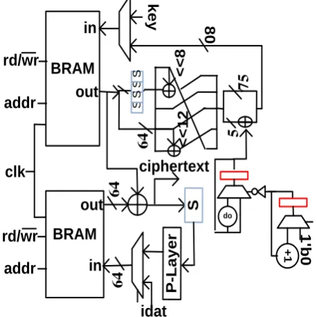
D. RAM-based Architecture
In this section, two RAM-based architectures are proposed. BRAM is used to store data and to generate S-boxes as a result registers, slices, and LUTs in the FPGA are free to be used for any other purpose.
Using RAM based S-Box: In this architecture, BRAM is
used to store data, key and to implement S-box. Two multiplexers are used to decide whether the user given input or processed intermediate data should be the input of BRAM. As shown in Fig. 8 in Data scheduling part of the architecture output of the BRAM is fed to a 64-bit XOR gate. Thereafter this output of XOR goes to another BRAM. Output of this BRAM is actually the value which should come after performing substitution in the given data. Then this output is permutated through hard-wired P-layer. As mentioned in [7], for silicon technology shifts and permutation do not require any cost for implementation.
[image:4.595.54.290.212.487.2]BRAM P -L a y e r 6 4 ciphertext clk rd/wr addr idat BRAM rd/wr addr 6 4 5 7 5 < < 1 2 < < 8 k e y + 1 op 1 'b 0 8 0 in in out out BRAM rd /w r c lk addr in BRAM addr c lk in rd /w r out o u t 6 4
Fig. 8. RAM-based Architecture of RECTANGLE cipher
with RAM-based S-box.
[image:4.595.310.543.438.707.2]International Journal of Innovative Technology and Exploring Engineering (IJITEE) ISSN: 2278-3075, Volume-8 Issue-10, August 2019
The output from P-layer gets stored in BRAM via a multiplexer. In key scheduling part of the design, rightmost 16-bits from the output of the BRAM are sent to S-box layer, which is stored in another BRAM module. Rest of the 64-bits is not processed. Thereafter generalized Feistel transformation is performed on the resultant 80-bits.
BRAM
P-L
a
y
e
r
6
4
S
ciphertext
clk
rd/wr
addr
idat
BRAM
rd/wr
addr
6
4
7
5
5
<
<
1
2
<
<
8
S
S
S
S
k
e
y
+
1
op
1
'b
0
8
0
in
in
out
out
6
[image:5.595.337.518.51.198.2]4
Fig. 9. RAM-based Architecture of RECTANGLE block cipher with Boolean S-box. BRAM is used to store key and data.
Using Boolean S-Box: As shown in Fig. 9, only
processed data and key are stored in BRAM. For storing data and key, BRAM of 64-bits and 80-bits are used respectively. S-boxes are not implemented using BRAM but by using slices and LUTs. Optimization in BRAM based S-box is difficult due to the rigid nature of the design [30]. In this work, Boolean logic is used to implement S-boxes. One clock cycle is required to take the input and another to generate output. Additional 2 clock cycles are required to complete a single round of encryption. This leads to a total latency of 50 clock cycles.
E. Iterative design with partial loop unrolling
In this work, 5 rounds of RECTANGLE cipher are unrolled and chained together with no registers in between. Data is passed serially through the five rounds. As shown in Fig. 10, a common 64-bits register is used to hold the input and intermediate data. To complete the encryption, iterations are repeated five times. The objective behind this work is to obtain an optimum trade-off between area and performance. Round subkeys are pre-generated and stored in a ROM module. Keys are retrieved from ROM, according to the round. This design can be implemented through pipeline as well, with the introduction of registers. A similar approach is reported by the authors in [31]. But the introduction of registers will increase area a lot. Disadvantage of this design is that architecture is vulnerable to side channel attack.
Round1 D 0 1
64
idat
ciphertext 64 Round5 Round4 Round3 Round2
ld
S U B K E Y S
0 1 D +1
addr 64
64
64 64
64
Fig. 10. Iterative Architecture with Partially loop unrolled
IV. SIMULATIONPLATFORM
A. Environment
All the RECTANGLE architectures were modeled using Verilog and synthesized for Xilinx FPGAs using ISE design suite 14.6. Different FPGA platforms are used to implement, compare and evaluate the architectures. For implementation in LUT-4 FPGA, Spartan-3(xc3s4000l-4fg900) and Virtex-4 (xc4vlx25-12ff668) were considered. For implementation in LUT-6 FPGA, Spartan-6 (xc6slx16-3csg324) and Virtex-5 (xc5vlx50t-3ff1136) platforms were considered. For performing power analysis Xilinx tool XPower Analyzer is used. In evaluation newer 7 series FPGA are not considered as their configurable logic block (CLB) is very similar to 6 series FPGA leading to replication of implementation results [35].
B. Configuration
Source code for implementation of RECTANGLE block cipher round based architecture is provided by the authors in [8]. Source files are synthesized and implemented in different FPGA platforms to obtain the results. Design environment is kept constant while implementing the architectures so as to provide a fair comparison between all the architectures. All the designs are implemented with the same synthesis parameters and implementation criteria. Different configurations along with their key sizes are shown in Table I.
C. Metrics
In this work, for evaluation of architecture various metrics are considered. For resource estimation, Slices, Flip-flops and number of LUTs are taken into account. Resource usage for each design is estimated through implementation report generated by ISE design tool 14.6. All these metrics vary according to the type of FPGA used. Power consumption is calculated using the Xilinx XPower analyzer tool. It provides values of static, dynamic and total power consumed by the architecture. Analysis is done using user-defined operational frequency at default operation temperature. For all the studies operational frequency of 13.56 MHz is considered. Reason for this is low power devices do not work on maximum operational frequency but are limited to lower frequency. For example, in case of RFID tags, operational frequency is taken to be of 13.56MHz [36].
[image:5.595.55.284.143.372.2]Table- I: Different configurations of the RECTANGLE cipher
Architecture Key Size Conf.
Iterative Architecture 80 A1
Iterative Architecture 128 A2
16-bits Serial with key scheduling 80 A3
16-bits Serial with key scheduling 128 A4
RAM-based Architecture(on Slice) 80 A5
RAM-based Architecture(on RAM) 80 A6
Iterative design with partial loop unrolled 80/128 A7*
Base Architecture[8] 80 A8
* Results same for 80/128 bits architecture
Energy spent by the architecture to process a single block of data, for the frequency of 13.56 MHz is calculated according to (1):
Energy = Total Power x latency / 13.56 MHz (1) Energy will directly be affected by the latency of design if constant operational frequency is taken for all the architectures. For performance evaluation, both latency and throughput of the design is considered. Throughput is calculated according to (2) and (3):
Thr. = Block Size x FMax / Latency (2)
Thr.* = Block Size x 13.56 MHz / Latency (3)
Table- II: Presents resource usage and power consumption results for the architectures for different computing platforms
Conf. Key (bit)
Latency (Cycles)
Slic e
LU T
Flip Flop
FMax (MHz)
Static Pow(mW)
Dynamic Pow(mW)
Total Pow(mW)
Thr (Mbps)
Thr* (Mbps)
ENE* (µJ)
Thr*/slc (mbps/slc)
xc6slx16-3csg324 (Spartan-6)
A1 80 42 58 202 158 168.32
7
19.91 1.46 21.37 256.496 20.66 .066 .356
A2 128 48 85 300 203 172.39
1
19.91 1.80 21.71 229.797 18.08 .076 .212
A3 80 105 55 198 153 166.61
5
19.94 4.25 24.19 101.555 8.035 .187 .144
A4 128 108 80 275 203 164.20
6
19.92 2.90 22.82 93.827 7.961 .181 .096
A5 80 50 61 160 6 180.20
9
20.08 18.72 38.80 230.667 17.356 .143 .279
A6 80 50 83 110 6 135.02
2
20.10 20.46 40.56 172.829 17.356 .149 .184
A7 80/12
8
5 139 472 67 61.758 20.31 41.82 62.13 838.298 173.56 .022 .933
A8 80 26 76 272 149 286.11
1
20.29 39.09 59.37 704.273 33.37 .113 .514
xc5vlx50t-3ff1136 (Virtex-5)
A1 80 42 72 231 158 410.59
0
562.96 2.92 562.96 626.252 20.66 1.74 .317
A2 128 48 117 313 203 388.18
8
560.07 5.90 565.97 517.454 18.08 1.99 .194
A3 80 105 67 226 153 338.14
6
560.06 5.18 565.24 206.107 8.035 4.37 .118
A4 128 108 103 301 203 338.39
1
560.08 7.58 567.67 193.356 7.961 4.52 .078
A5 80 50 113 224 6 286.24
6
560.42 41.55 601.97 366.394 17.356 2.219 .158
A6 80 50 146 212 6 175.56
8
560.20 19.31 579.52 224.692 17.356 2.136 .098
A7 80/12
8
5 221 573 67 146.63
8
560.44 43.29 603.72 1876.96 173.56 .222 .784
A8 80 26 101 278 149 501.65
5
560.37 36.75 597.12 1234.54 33.37 1.144 .596
xc3s4000l-4fg900 (Spartan-3)
A1 80 42 174 312 158 102.55
4
268.29 6.68 274.97 156.217 20.66 .849 .118
A2 128 48 212 377 203 108.51
0
268.27 5.68 273.94 144.643 18.08 .967 .085
A3 80 105 186 350 153 93.519 268.16 1.58 269.73 57 8.035 2.088 .042
A4 128 108 252 365 203 94.917 268.14 1.14 269.28 54.235 7.961 2.144 .031
A5 80 50 173 262 6 141.25
3
268.54 15.80 284.34 181.149 17.356 1.048 .100
A6 80 50 166 218 6 141.12
3
268.84 26.90 295.74 180.637 17.356 1.090 .104
A7 80/12
8
5 361 624 67 37.046 268.71 58.68 328.39 474.188 173.56 .024 .476
A8 80 26 180 300 149 179.79
1
268.69 57.72 327.40 442.46 33.37 .627 .185
xc4vlx25-12ff668 (Virtex-4)
A1 80 42 173 311 158 247.39
1
233.03 16.36 249.39 376.974 20.66 .770 .119
A2 128 48 212 377 203 261.89
7
233.06 17.51 250.57 349.108 18.08 .884 .085
A3 80 105 186 350 153 224.55
8
232.89 8.71 241.60 136.872 8.035 1.87 .042
A4 128 108 253 365 203 222.62
0
232.99 14.22 247.21 127.205 7.961 1.97 .031
A5 80 50 170 261 6 261.21
9
233.66 49.31 282.97 334.360 17.356 1.043 .100
A6 80 50 166 217 6 167.79
4
233.61 46.65 280.26 214.776
3
17.356 1.033 .104 A7 80/12
8
5 361 624 67 99.698 233.79 56.21 290 1276.13
4
173.56 .022 .480
A8 80 26 180 300 149 494.03
5
International Journal of Innovative Technology and Exploring Engineering (IJITEE) ISSN: 2278-3075, Volume-8 Issue-10, August 2019
Here, Throughput (thr) is maximum throughput of the design and depends on the maximum operational frequency and latency of the architecture. Throughput*(Thr*) is calculated using an operational frequency of 13.56 MHz.
Throughput/slice (thr*/slc) is a derived metric. It is estimated to study how efficient a design is when trade-off between implementation size and performance is desired [2]. It is simply calculated by dividing throughput obtained at a frequency of 13.56 MHz. with the number of slices utilized in the implementation of the architecture.
V. RESULTSANDDISCUSSION
Table II illustrates resource requirement, performance, energy utilization and power consumption for all the implementations. Results are evaluated and compared for all the four FPGAs.
Performance parameter and resource consumption changes according to the type of FPGA used for implementation of the architecture. Fig. 11 shows a graphical representation of resource consumption for all the FPGA platforms. It is observed, for both LUT-4 FPGA resource utilization remains nearly constant.
[image:7.595.63.539.199.354.2](a) (b) (c)
Fig. 11. Resource consumption for all the architectures (a) Slices (b) LUTs (c) Flip-Flops
(a) (b)
[image:7.595.108.488.400.665.2](c) (d)
Fig. 13. Throughput obtained for all the architectures using different platforms at (a) Maximum operational frequency (b) Frequency of 13.56 MHz
While for LUT-6 FPGA, there is variation in resource consumption. Spartan-6 uses less number of slices for implementation as compared to Virtex-5. This is due to variation in architecture design of the slices in the FPGA. The best result for resource consumption is given by Spartan-6 FPGA. The number of flip-flops utilized by any architecture remains consistent for all the platforms.
Number of flip-flops used is least for BRAM based architecture (A5/A6) followed by Iterative design with partial loop unrolling (A7). Least number of slices is used by 16-bit architecture with 80-bits key scheduling (A3) for Spartan-6 FPGA, with reduction of 38.18% as compared to base architecture (A8). Iterative design (A1) gives 55.03% reduction in the number of flip-flops and 34.65% reduction in the number of LUTs as compared to A8. In RAM based Architecture (A5/A6), the number of flip-flops needed for implementation is reduced by 96.07 % as compared to 16-bits architecture with 80-bit key scheduling (A3). This reduction in number of flip-flops remains the same for all four FPGAs. Remaining unused flip-flops are free to be used for any other purpose. On implementing S-box in BRAM (A6), resource consumption is reduced further. For Spartan-6, number of LUTs in A6 is reduced by 41.17% as compared to A8.
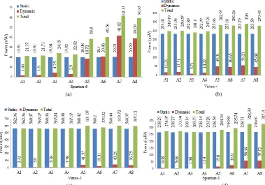
Fig. 12 illustrates power consumption for all designs. It is observed that static power remains nearly constant for all the architectures. Dynamic power changes due to switching activity of the FPGA. Power analysis shows variation based on the type of FPGA used for the implementation of the architecture. Implementation in Virtex-5 FPGA requires less dynamic power and more static power as compared to Virtex-4. It is observed any architecture implemented in Spartan-6 FPGA requires relatively less power consumption than any other FPGA. Iterative designs (A1/A2) required less power consumption for their implementation in LUT-6 FPGA. While for LUT-4 FPGA RAM based designs require less power.
Fig. 13 provides an illustration of throughput obtained for all the designs. It is seen that the best throughput results for maximum operational frequency as well as for frequency of 13.56 MHz are given by A7. In this design, latency is also less than other architectures. As compared to A8, latency of A7 is decreased by 80.76%. Throughput (Thr*) of A7 is 5.20 times that of A8. Best value of throughput at maximum operational frequency is given for Virtex-5 platform. For this
FPGA, throughput is increased by 52.03% as compared to A8. Throughput of designs at a frequency of 13.56 MHz remains same for all the FPGA platforms.
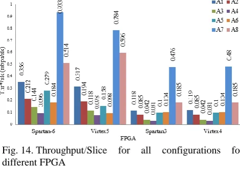
Fig. 14 shows the graphical representation of throughput per slice obtained for different FPGA platforms. The advantage of A7 is that it requires just five clock cycles for generating the result. So, it gives good throughput for all four FPGA platforms. A7 gives best trade-off between resource consumption and throughput. Best value for throughput per slice is given for Spartan-6 platform. For LUT-4 FPGA, throughput per slice of A7 becomes nearly 2.6 times that of A8.
Least energy consumption is taken by A7 in all the four platforms. Energy requirement in A7 is reduced by nearly 80% as compared to A8 for all FPGA. However, while comparing architectures with ROM based key schedule (A7) with other designs, security concerns due to side channel attack should be kept in mind.
Fig. 14. Throughput/Slice for all configurations for different FPGA
VI. CONCLUSION
In this work evaluation and comparison of different hardware architectures of RECTANGLE block cipher is presented. All the architectures are implemented in four different FPGA platforms. Results are evaluated with similar implementation tools and design environment. This leads to a fair evaluation of all the designs in a given FPGA platform. It is observed that Spartan-6 FPGA provides the least
resource and power
[image:8.595.310.545.465.632.2]International Journal of Innovative Technology and Exploring Engineering (IJITEE) ISSN: 2278-3075, Volume-8 Issue-10, August 2019
16-bit architecture with the 80-bits key schedule (A3) is a good alternative if area/security trade-off is required. If the requirement is of higher security, architecture with 128-bits key schedule (A2/A4) is desirable. Iterative architecture (A1) is providing a good trade-off between throughput per slice and energy requirement. RAM-based architecture (A5/A6) needs the least number of registers for its implementation. Best trade-off among throughput and area is given by Iterated design with partial loop unrolling (A7). It also gave the best energy consumption results for all four FPGA platforms. All the architectures have different power consumption and have different requirement of resources for their implementation in different FPGA platforms. According to the requirement, appropriate architecture can be selected for an application.
REFERENCES
1. P. Pawar, and A. Trivedi, “Device-to-Device Communication Based IoT System: Benefits and Challenges.” IETE Technical Review, 2018, pp.1-13.
2. C. A. Lara-Nino, A. Diaz-Perez, and M. Morales-Sandoval, “Lightweight hardware architectures for the present cipher in FPGA.” IEEE Transactions on Circuits and Systems I: Regular Papers, vol. 64, no. 9, 2017, pp.2544-2555.
3. A. A. R. Haeri, M. G. Karkani, M. Sharifkhani, M. Kamarei, and A. Fotowat-Ahmady, “Analysis and design of power harvesting circuits for ultra-low power applications,” IEEE Trans. Circuits Syst. I, Reg. Papers, vol. 64, no. 2, 2017, pp. 471–479, Feb.
4. Z. Zou, D. S. Mendoza, P. Wang, Q. Zhou, J. Mao, F. Jonsson, H. Tenhunen, and L. R.Zheng, “A low-power and flexible energy detection IR-UWB receiver for RFID and wireless sensor networks,” IEEE Trans. Circuits Syst. I, Reg. Papers, vol. 58, no. 7, pp. 1470–1482, Jul. 2011. 5. C. Alippi, and C. Galperti, “An adaptive system for optimal solar energy
harvesting in wireless sensor network nodes,” IEEE Trans. Circuits Syst. I, Reg. Papers, vol. 55, no. 6, pp. 1742–1750, Jul. 2008. 6. M. Kar, A. Kumar, D. Nandi, and M. K. Mandal “Image encryption
using DNA coding and hyperchaotic system”, IETE Technical Review, 2018, pp.1-12.
7. N. F. Pub, "197: Advanced encryption standard (AES)," Federal Information Processing Standards Publication, vol. 197, pp. 0311, 2001. 8. D. E. Standard, "Federal information processing standards publication 46," National Bureau of Standards, US Department of Commerce, vol. 23, 1977.
9. A. Bogdanov, L. R. Knudsen, G. Leander, C. Paar, A. Poschmann, M. J. Robshaw, Y. Seurin, and C. Vikkelsoe, "PRESENT: An ultra-lightweight block cipher," in International Workshop on Cryptographic Hardware and Embedded Systems, vol. 4727. Berlin Germany: Springer, 2007, pp. 450-466.
10. Z. Xiang, W. Zhang, Z. Bao, and D. Lin, "RECTANGLE: a bit-slice lightweight block cipher suitable for multiple platforms," Science China Information Sciences, vol. 58, 2015, pp. 1-15.
11. Z. Gong, S. Nikova, and Y. W. Law, "KLEIN: a new family of lightweight block ciphers," International Workshop on Radio Frequency Identification: Security and Privacy Issues, vol. 7095, 2011, pp. 1-18.
12. J. Guo, T. Peyrin, A. Poschmann, and M. Robshaw, “The LED block cipher,” in International workshop on cryptographic hardware and embedded systems, vol. 6917, 2011, pp. 326–341.
13. C. H. Lim, and T. Korkishko, "mCrypton–a lightweight block cipher for security of low-cost RFID tags and sensors," in International Workshop on Information Security Applications, 2005, pp. 243-258.
14. T. Shirai, K. Shibutani, T. Akishita, S. Moriai, and T. Iwata, "The 128-bit block cipher CLEFIA," in International Workshop on Fast Software Encryption, 2007, pp. 181-195.
15. R. Beaulieu, S. Treatman-Clark, D. Shors, B. Weeks, J. Smith, and L. Wingers, "The SIMON and SPECK lightweight block ciphers," in Design Automation Conference (DAC), 52nd ACM/EDAC/IEEE, 2015, pp. 1-6.
16. K. Shibutani, T. Isobe, H. Hiwatari, A. Mitsuda, T. Akishita, and T. Shirai, "Piccolo: an ultra-lightweight block cipher," in International Workshop on Cryptographic Hardware and Embedded Systems, 2011, pp. 342-357.
17. T. Suzaki, K. Minematsu, S. Morioka, and E. Kobayashi, "Twine: A lightweight, versatile block cipher," in ECRYPT Workshop on Lightweight Cryptography, 2011.
18. W. Wu, and L. Zhang, "LBlock: a lightweight block cipher," in International Conference on Applied Cryptography and Network Security, 2011, pp. 327-344.
19. B. S. Shankar, and S. Tripathy. "Securing Multicast Group Communication in IoT-Enabled Systems." IETE Technical Review, vol. 36, issue 1, pp.83-93, 2018.
20. B. N. Silva, M. Khan, and K. Han, “Internet of Things: A Comprehensive Review of Enabling Technologies, Architecture, and Challenges”, IETE Technical Review, vol. 35, issue 2, pp. 205-220, 2017
21. T. Xu, J. B. Wendt, and M. Potkonjak, “Security of IoT systems: Design challenges and opportunities,” in Proc. IEEE/ACM Int. Conf. Comput.-Aided Design (ICCAD), Piscataway, NJ, USA, Nov. 2014, pp. 417–423.
22. T. Tuan, S. Kao, A. Rahman, S. Das, and S. Trimberger, “A 90nm low-power FPGA for battery-powered applications,” in Proc. of the 2006 ACM/SIGDA 14th international sym. on FPGA. New York, NY, USA: ACM, 2006, pp. 3–11.
23. T. Good, and M. Benaissa, “Very small FPGA application-specific instruction processor for AES,” IEEE Trans. Circuits Syst. I, Reg. Papers, vol. 53, no. 7, pp. 1477–1486, Jul. 2006.
24. P. Yalla, and J.-P. Kaps, “Lightweight cryptography for FPGAs,” in Proc. Int. Conf. Reconfigurable Comput. FPGAs (ReConFig), Dec. 2009, pp. 225–230.
25. J. A. Galaviz-Aguilar, J. C. Nuñez-Perez, F. J. Perez-Pinal, and E. Tlelo-Cuautle "FPGA Realisation of n-QAM Digital Modulators." IETE Technical Review, DOI: 10.1080/02564602.2018.1470038, 2018. 26. N. Smyth, M. McLoone, and J. V. McCanny, “WLAN security
processor,” IEEE Trans. Circuits Syst. I, Reg. Papers, vol. 53, no. 7, pp. 1506–1520, Jul. 2006.
27. E. B. Kavun, and T. Yalcin, “RAM-based ultra-lightweight FPGA implementation of PRESENT,” in Proc. Int. Conf. Reconfigurable Comput. FPGAs (ReConFig), 2011, pp. 280–285.
28. C. A. Lara-Nino, M. Morales-Sandoval, and A. Diaz-Perez, "Novel FPGA-based low-cost hardware architecture for the PRESENT block cipher," in Proc. Euromicro Conference on Digital System Design (DSD), 2016, pp. 646-650.
29. N. Hanley, and M. O’Neill, “Hardware comparison of the ISO/IEC 29192-2 block ciphers,” in Proc. IEEE Comput. Soc. Annu. Symp. VLSI (ISVLSI), Aug. 2012, pp. 57–62.
30. J. J. Tay, M. L. D. Wong, M. M. Wong, C. Zhang, and I. Hijazin, “Compact FPGA implementation of PRESENT with Boolean S-Box,” in Proc. 6th Asia Symp. Quality Electron. Design, Aug. 2015, pp. 144–148.
31. A. J. Elbeirt, and C. Paar, “An FPGA implementation and evaluation of the Serpent block cipher”, in FPGA `00 Proceedings of the 2000 ACM /SIGDA eighth international symposium on field programmable gate arrays, Feb. 2011, pp. 33-40.
32. A. Moradi, A. Barenghi, T. Kasper, and C. Paar, “On the vulnerability of FPGA bitstream encryption against power analysis attacks: Extracting keys from Xilinx Virtex-II FPGAs,” In Proceedings of the 18th ACM conference on Computer and communications security, 2011, pp. 111–124.
33. M. Nassar, Y. Souissi, S. Guilley, and J.-L. Danger, “‘Rank correction’: A new side-channel approach for secret key recovery,” In International Conference on Security Aspects in Information Technology. Berlin, Germany: Springer, 2011, pp. 128–143.
34. S. Gao, H. Chen, W. Wu, L. Fan, W. Cao, and X. Ma, “My traces learn what you did in the dark: Recovering secret signals without key guesses,” . In Cryptographers’ Track at the RSA Conference. Cham, Switzerland: Springer, 2017, pp. 363–378.
35. (Sep. 2016). 7 Series FPGAs Configurable Logic Block. [Online]. Available: www.xilinx.com
AUTHORSPROFILE
Nivedita Shrivastava received her bachelor’s degree in Electronics and Telecommunication Engineering from Jabalpur Engineering College, Jabalpur, India. Currently, she is an M.Tech. student pursing degree in VLSI and Embedded System from National Institute of Technology Raipur, India. Her main area of interest is the Design and Implementation of highly optimized cryptographic algorithms for constrained resource environment.