Faculty of Health, Engineering and Sciences
Optimisation of Multicore Processor and GPU for use in Embedded
Systems
A dissertation submitted by
Chloe Mansell
In fulfilment of the requirements of
ENG4112 Research Project
towards the degree of
The advancement in technology continues to consume an increasing part of our lives and as we watch the slowing of Moore’s Law as Integrated Circuits approach physical limitations, we will continue to search for faster execution of programs.
The advancement in robotics and machine vision will see them become part of our daily lives and the need for real time machine vision algorithms will increase.
Faculty of Health, Engineering and Sciences
ENG4111/ENG4112 Research Project
Limitations of Use
The Council of the University of Southern Queensland, its Faculty of Health, Engineering & Sciences, and the staff of the University of Southern Queensland, do not accept any responsibility for the truth, accuracy or completeness of material contained within or associated with this dissertation. Persons using all or any part of this material do so at their own risk, and not at the risk of the Council of the University of Southern Queensland, its Faculty of Health, Engineering & Sciences or the staff of the University of Southern Queensland.
Faculty of Health, Engineering and Sciences
ENG4111/ENG4112 Research Project
Certification of Dissertation
I certify that the ideas, designs and experimental work, results, analyses and conclusions set out in this dissertation are entirely my own effort, except where otherwise indicated and acknowledged.
I further certify that the work is original and has not been previously submitted for assessment in any other course or institution, except where specifically stated.
Firstly I would like to extend my thanks and appreciation to my supervisor Stephen Rees who has always been available when needed and has offered valuable input and feedback.
Abstract i
Acknowledgments iv
List of Figures List of Tables Chapter 1 Introduction 1
1.1 Research Aim . . . 2
1.2 Objectives . . . 2
1.3 Overview of Dissertation . . . 2
1.4 Background Information . . . 4
1.4.1 Common Embedded Systems. . . 4
1.4.2 What is Optimisation . . . 19
1.4.3 Why Optimise . . . 19
Chapter 2 Literature Review 21
2.1 Software Optimisation techniques . . . 21
2.1.1 Software techniques . . . 21
2.1.2 Compiler Optimisations . . . 22
2.1.2.3 Loop unrolling . . . .23
2.1.2.4 GCC optimisation options . . . 24
2.1.3 Source code modifications . . . 26
2.1.3.1 Loop termination . . . 26
2.1.3.2 Loop Fusion . . . 26
2.1.3.3 Variable Selection . . . 27
2.1.3.4 Pointer aliasing . . . 27
2.1.3.5 Division and modulo . . . 27
2.1.4 Software Optimisation Conclusion . . . 28
2.2 Optimising with Hardware . . . 29
2.2.1 Neon Data Engine . . . 29
2.2.2 Graphics Processing Unit . . . 31
Chapter 3 Methodology 33
3.1 Research and Development methods . . . 33
3.2 Task analysis . . . . . . 34
3.3 Risk Assessment . . . 35
3.3.1 Risk Identification . . . 35
3.3.2 Risk Evaluation . . . 35
3.4.1 Research and reporting . . . .37
3.4.2 Software development and Hardware testing . . . 37
3.5 Project Timeline . . . 39
Chapter 4 Software Development 40
4.1 Optimisation Techniques . . . 41
4.2 Image Processing . . . .. . . 42
4.3 Grey Scale Thresholding . . . 41
4.4 Average Smoothing Filter . . . .52
4.5 Testing . . . .60
Chapter 5 Results and Discussion 61
5.1 Grey Scale Thresholding . . . .. 61
5.11 Results . . . . .. . . 62
5.2 Average Smoothing Filter . . . 71
5.2.1 Results . . . .72
5.3 Conclusion . . . . . . 80
Chapter 6 Conclusion and Further Work 82
References 83
Appendix A Project Specification 87
Appendix D Output photos from Grey Scale Algorithm 132
1.1 Harvard architecture . . . 5
1.2 Von Neumann architecture . . . 5
1.3 Arm Cortex A7 . . . .7
1.4 Cortex A7 Pipeline . . . .7
1.5 Arm Cortex A15 . . . .8
1.6 Cortex A15 Pipeline . . . .8
1.7 Scalar add vs SIMD parallel add . . . .9
1.8 Neon registers . . . 10
1.9 Single Precision floating-point format . . . .11
1.10 Circular buffer operation . . . .13
1.11 Typical DSP architecture . . . 14
1.12 FIR filter steps . . . .15
1.13 FPGA . . . .16
1.14 Comparison between CPU and GPU cores . . . .17
1.15 Computer vision vs computer graphics . . . 18
1.16 Arm Mali – T628 . . . .18
2.1 Example of loop . . . .24
2.2 Example of loop unrolled . . . .24
2.3 Example of unmerged and merged loops . . . .27
3.1 ODROID XU3 Development Board . . . .38
4.2 Grey Scale threshold development code. . . 45
4.3 Loop reversal for greyscale threshold . . . 46
4.4 Loop unrolling excerpt . . . 47
4.5 For loop within grey scale threshold program . . . 48
4.6 Block of code directing process through single core . . . 48
4.7 Loop for Neon data engine . . . 50
4.8 Convert greyscale image to RGB code . . . .51
4.9 Smoothing filter algorithm . . . 52
4.10 Original image used for image processing . . . 53
4.11 Image after alterations from average smoothing filter . . . 53
4.12 Average Smoothing Filter program . . . 54
4.13 Loop for average smoothing filter with loop unrolling . . . .56
4.14 Load and sum functions in average smoothing filter . . . 58
4.15 Copy of program section which calculates execution time . . . .60
5.1 Image prior to image processing . . . .. . . 61
5.2 Output image from Grey Scale thresholding . . . . .62
5.3 Grey Scale Thresholding Graph . . . .69
5.4 Grey Scale Thresholding Graph without GPU . . . 70
5.1 Results from Grey Scale Thresholding Program . . . .62
5.2 Results from Grey Scale Thresholding with loop reversal . . . 63 5.3 Results from Grey Scale Thresholding with loop unrolling . . . 64
5.4 Results from Grey Scale Thresholding with pointer Optimisation. 64 5.5 Results from Grey Scale Thresholding pointer and loop unrolling 65 5.6 Results from Grey Scale Thresholding Pointer and loop reversal.. 66
5.7 Results from Grey Scale Thresholding directed through A7 Core. 66 5.8 Results from Grey Scale Thresholding directed through A15 core..67
5.9 Results from Grey Scale Thresholding directed through Neon . . . 68 5.10 Results from Grey Scale Thresholding directed through GPU . . . 69 5.11 Results from Average Smoothing Filter . . . .72
5.12 Results from Average Smoothing Filter with loop reversal . . . .72 5.13 Results from average smoothing filter with loop unrolling . . . .73
5.14 Results from average smoothing filter with pointer optimisation . 74 5.15 Results from average smoothing filter with pointer and reversal. . 74
5.18 Results from average smoothing filter directed through A15 . . . . 76
Abbreviations
DSP Digital Signal Processor
FPU Floating Point Unit
SIMD Single instruction stream multiple data stream GPU Graphics processing unit
RISC Reduced instruction set computer CISC Complex instruction set computer
Introduction
The advancement of technology has been continuing at a rate predicted by Moore’s Law half a century ago. Continued advancements including the decrease in the size of integrated circuit components allowing more components on a single chip has decreased the cost of processors and greatly improved performance including clock speeds and power efficiency.
We are now seeing the slowing of Moore’s Law as advancement’s in Integrated Circuits approach physical limitations. This slowing has contributed in the birth of multicore processors and parallel processing to allow for continued increase in processing power. As the cost of multicore processors and development boards become lower this will allow multicore processors to become more of a viable option for use in embedded systems.
This dissertation will investigate the use of multicore processors and Graphics Processing Unit to execute optimised embedded system algorithms.
1.1
Research Aim
The aim of this project is to investigate how to optimise a multicore processor and its ancillary computational hardware, for use in an embedded system. The project will determine if there is an advantage in using a range of optimisation software techniques combined with manually directing data through the Central Processing Unit, Neon unit and the Graphics Processing unit, in comparison to allowing the compiler to schedule the optimise code and direct the data.
1.2 Objectives
1. To develop a software program which will benchmark computational speeds of different components on the ODROID XU3 development board.
2. Test the development board with software programs containing typical machine vision algorithms and record execution speeds. 3. Analyse and benchmark the data obtained.
1.3
Overview of Dissertation
The dissertation has been broken up into the following chapters. Chapter 1: Introduction
Chapter 2: Literature Review
The literature review will review current literature on software optimisation techniques which will assist in the decision on what techniques will be used on the software code for the purpose of this dissertation. The review will also investigate the current literature covering the use of hardware components including the Neon Data engine and Graphics processing unit to further improve on execution speeds of the software program.
Chapter 3: Methodology
Chapter three contains research and development methods as well as a task analysis outlining milestones for the project. This is followed by a Risk assessment, Resource analysis and Project timeline.
Chapter 4: Software Development
Chapter four will outline the development of each software program and how the algorithms were approached.
Chapter 5: Results and Discussion
Chapter five will show the results from the execution of the software and analysis of the results.
Chapter 6: Conclusion and further work
1.4
Background Information
This section will cover the background information required to obtain an in-depth understanding of current processors used in embedded systems. Optimisation and why optimisation is required will also be examined.
1.4.1
Common embedded systems
Microcontroller
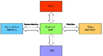
A microcontroller can be described as a computer on a single chip containing simplified elements which are able to perform less complex applications. The microcontroller is a smaller more economical options which has been typically used in the use of embedded systems (Bates 2011, p.17). A microcontroller will contain a central processing unit, memory and access to input data and the ability to output data. The following background information will cover a range of processing units available to be used to perform the tasks required in a real time system.
Central Processing Unit (CPU)
storage spaces and two buses this allows simultaneous transfer of instructions and data as well as allowing the instruction and data sizes to be different (USQ, 2013).
Figure 1.1 Harvard architecture (USQ 2013, p.137)
[image:20.595.207.382.159.254.2]The second major architecture available is the Von Neumann architecture which has one place for storage hence the data and instructions are stored within the same memory. As there is only one storage unit available there is also only one bus for the information to move from memory to the control unit not allowing for simultaneous transfer of instructions and data. Movement between these units will consequently need to be scheduled and the size of the data and instruction will need to be the same length (USQ, 2013).
Figure 1.2 Von Neumann architecture (USQ 2013, p.136)
two on board memory caches added. There is a cache available for instruction memory and one available for data memory and each has a common address space that share the one memory. The modified Harvard architecture allows the processor to perform similar to a Von Neumann when accessing memory and similar to a Harvard when accessing the caches.
Other terms which are common when discussing different forms of CPU’s are the type of instructions sets which are used when programming. The two distinct types are CISC architecture which stands for a complex instruction set computer and RISC which stands for a reduced instruction set computer.
A CISC is a complex set of instructions and therefore there are more instruction available to use then the RISC set, this allows the programmer to write less code to perform the same task when compared to a RISC (USQ, 2013). This however is not always appropriate in an embedded system as more transistors are required on the chip and there is also a higher power consumption and heat dissipation when using this form of architecture. Therefore a RISC architecture would be a more appropriate choice for microcontrollers when used in embedded or mobile applications. This is seen in the ARM architectures which is a popular set of RISC microcontrollers which can be found in 95% of smart phones, 80% of digital cameras and 35% of all electronic devices (ARM, 2014).
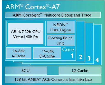
A7 – CPU
Figure 1.3 Arm Cortex A7 (ARM 2015)
The Cortex A7 has an in order, non-symmetric dual issue processor with a pipeline length between 8 to 10 stages (ARM 2015). The chip contains hardware for SIMD in the Neon data engine, a floating point unit and two on board cache.
Figure 1.4 Cortex A7 Pipeline (Electronic Design 2011).
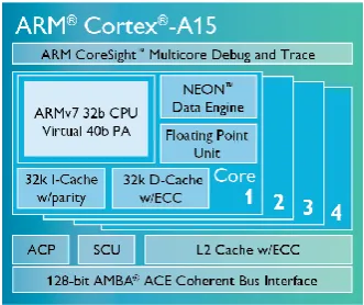
[image:22.595.221.367.431.522.2]A15 – CPU
Figure 1.5 ARM Cortex A15 (ARM 2015)
[image:23.595.214.380.103.242.2]The Cortex A-15 is a high end triple issue, out of order processor core. The A15 has the ability to implement virtualisation instructions, hardware-accelerated integer division and also a 40 bit virtual memory addressing extensions (ARM 2015). The A15 also contains a SIMD unit in the Neon data engine and floating point unit as well as two on board cache.
Figure 1.6 Cortex A15 Pipeline (Electronic Design 2011).
SIMD – Single Input Multiple Data
SIMD or Single Instruction Stream Multiple Data Stream allows the same operation to be performed on Multiple Data at the same time (Zhou & Shi 2008).
SIMD will allow a single instruction to split a register into multiple data elements which will allow multiple identical operations on these elements. The following figure 2.1 illustrates the difference between a scalar add and a SIMD parallel add (ARM 2013).
Figure 1.7 Scalar add vs SIMD parallel add (ARM 2013).
SIMD operations are available to use on a variety of CPU’s through
operations. The registers can either be made up of 16 x 128 bit or 32 x 64 bit registers (ARM 2013).
Figure 1.8 Neon registers (ARM 2015)
NEON has the following data types available: - Unsigned integer U8 U16 U32 U64. - Signed integer S8 S16 S32 S64
- Integer of unspecified type I8 I16 I32 I64 - Floating-point number F16 F32
- Polynomial over {0,1} PS
(ARM 2013) Processing data in NEON can be done in either Normal, Long, Wide,
Floating Point Unit (FPU)
Each core in both the Arm A7 and A15 processors contain a Floating Point Unit which can be used when it has been enabled otherwise any Floating point calculations will be done through the use of library functions. (ARM 2013). As per the IEEE-754 standard floating point numbers are represented within the Arm Cortex A series hardware as follows:
Figure 1.9 Single Precision floating-point format (ARM 2013)
S = Sign Bit which indicates if the number is positive or negative
Exponent gives the order of the magnitude of the number and the Mantissa is the fractional binary digits of the number. If the number is a single precision float the number is stored as per figure 2.10. The conversion to a single 32 bit float may cause a loss of precision if the number being stored cannot be represented wholly within the 23 bit mantissa. In this case the use of a double-precision floating point number may be appropriated as it has an exponent field with 11 bits and a mantissa with 52 bits (ARM 2013).
Both the Cortex A7 and A15 have the VFPv4 Floating point micro-architecture and the following registers:
- Thirty two or sixteen double-word registers (ARM 2013).
-
Floating point system ID register (FPSID) which is used to-
Floating point status and control registers (FPSCR) which are used to hold comparison results, flags for exceptions, select rounding options and enable floating point exception trapping (ARM 2013).-
Floating point Exception register (FPEXC) which is used to enable system software which controls exceptions which determine what has happened (ARM 2013).-
Media and VFP feature register 0 and 1 (MVFR0 and MVFR1) which enable software which determines what features from Floating point or SIMD are implemented on the processor (ARM 2013).Digital Signal Processor (DSP)
A Digital signal processor or DSP is a programmable microcontroller which has been designed to manipulate a stream of real time digital data usually in the form of a signal. A DSP is often used in processing audio, video and graphics processing (Thompson, 2001).
A DSP is designed to perform data manipulation and mathematical calculations at a rate fast enough to allow usage in a real time system and will have the following characteristics.
- Specialised high speed arithmetic
- A form of data transfer from and to the real world - A memory architecture which will allow multiple access
A DSP will often be used in digital signals to apply a digital filter to a signal to allow the signal to be free from distortion, interference or it may be used to separate two signals. This process involves taking samples of a signal, performing arithmetic to this sample and outputting the modified signal all in real time, therefore the DSP needs to perform large calculations fast. The signal will be represented by an equation for example the input will be x(n) and the output will be equal to y(n). The following is an example of an equation to find the output signal from a DSP with a FIR digital filter applied.
0 1 2
( ) (n) ( 1) ( 2) ...
y n a x a x n a x n (1.1)
The number of coefficients in this equation could be a number in the thousands and the DSP may be sampling a large amount of samples of the signal every second. To enable the DSP to do this it uses a circular buffer where it will store each coefficient for example x(n-1) where n-1 represents a past input separately within the buffer. As the time moves forward only one coefficient needs to be added and therefore only one value needs to be updated and not every coefficient within the equation (Smith, 1997).
In Figure 1.1 smith shows an example of how the circular buffer is used and how only one value x(n) is added which replaces the oldest value x(n-7). This allows the DSP to perform these calculations in real time and allows there to be no obvious delay between the readings of the information from the input signal to the output of the filtered signal (Smith 1997).
A DSP has a modified Harvard architecture which contains two data busses, one for the instructions and one for data. The DSP also has an instruction cache which will allow the storage of all the recent program instructions as seen in Figure 1.2. As the DSP performs the same repetitive instructions when sampling data, the DSP will retrieve the instructions from the cache after the first loop. Once the DSP is receiving instructions from the on board cache the memory transfer can be achieved within a single loop.
The DSP is now capable of receiving the sample from the signal from the data memory bus, the coefficients from the program memory bus and the instructions from the cache in parallel (Smith 1997).
A DSP will also allow access to the Multiplier, ALU and shifter to be accessed in parallel. (Smith 1997). In the following figure 1.3 Smith outlines the following steps in a DSP cycle when applying an FIR filter.
Figure 1.12 FIR filter steps (Smith 1997)
Once the beginning steps 1 – 5 are carried out Steps 6-14 may be carried out simultaneously within a single clock cycle which will allow a calculation for 100 coefficients to be performed in approximately 105-110 clock cycles.
Programmable Logic Devices
A logic device is a circuit which will accept either a logic 1 or logic 0 or a combination and return an output of either a 1 or a 0 (USQ 2013). A programmable logic device is a block of logic devices which are organised in a way to perform a particular task. They can be known as a Complex programmable logic device (CPLD), Field programmable gate array (FPGA) as well as many others.
and outputs through a global interconnection matrix. This matrix can be changed as necessary to allow different connections between blocks. There is the ability to connect input and output to these devices. The blocks can be programmed to perform logic functions such as OR, AND, NAND, NOR etc.
A field programmable gate array (FPGA) is a controller which consists of an array of logic blocks surrounded by input and output blocks. The logic blocks in an FPGA will implement the logic whilst programmable interconnect wires connect the inputs and outputs to the logic blocks as seen in Figure 1.3. Combined with the ability to be reprogrammed an FPGA can be very flexible and is often used in systems such as software-defined radio, aerospace and defence systems as well as medical imaging, computer vision and speech recognition (National Instruments 2014).
GPU’s – Graphics processing unit
A graphics processing unit is a multi-processor which has been designed for use in graphics processing. As a GPU is designed to process graphics which can include the process of thousands of pixels at one time they have a parallel architecture with thousands of small cores which are designed to all work simultaneously. This massive parallel processing is now being identified to be useful in applications other than graphics processing including scientific computation (NVidia 2015).
Figure 1.14 Comparison between CPU and GPU cores (NVidia 2015)
Figure 1.15 Computer vision vs computer graphics (Pulli et al. 2012)
The ability to partially program the GPU was created by the addition of shaders which allows data to be shared with the CPU and not sent directly to the display via a fixed-function pipeline (Pulli et al. 2012).
Writing parallel programs to utilise the GPU can be extremely difficult and complex which has seen the development of specific languages such as OpenCL, OpenGL and CUDA to assist programmers.
The GPU on the ODROID XU3 is the Arm Mali –T628 as shown in figure 1.15.
Figure 1.16. Arm Mali –T628 (ARM 2015)
1.4.2
What is optimisation?
Optimisation is when a process or task is designed to be the most efficient it can be. In computing terms this can be done through various techniques either by optimising the software code or through the use of various hardware units depending on the task at hand. For example a Digital signal processor would be used to apply a filter to a signal as this is the most efficient hardware available for this task.
Software optimisation is optimising the process through programming techniques such as; the use of registers, the removal of any dead code, the use of pointers and unrolling of loops to name a few. Appropriate software techniques will be looked at in more detail in the next chapter. In an embedded system optimisation can be used to increase the speed of the execution of code, increase the performance of battery life, code density or reducing the memory footprint of the code (Arm 2013).
1.4.3
Why optimise
Optimisation is important when in terms of embedded systems as it is typically required to operate in a real time environment, therefore the process will need to seem instantaneous for it to be affective.
Literature Review
In an embedded system optimisation is typically used to reduce the execution time of a program, reduce battery life, code density or the memory footprint (Arm 2013). For the purpose of this dissertation optimisation will be used to increase the speed of the code being executed. This section will cover possible optimisation techniques available to be used in conjunction with the ARM A series processors A7 and A15 as well as the ARM Mali T-628 GPU, this will also include the use of the NEON and FPU units included on the A7 and A15 processors.
2.1
Software
Optimisation techniques
2.1.1
Profiling
dissertation will be limited to a single set of calculations representing the 10 percent of code, profiling will therefore not be necessary.
2.1.2
Compiler Optimisations
GCC-4.8 will be the compiler which will be used to compile code on the development board. The Arm A-series Programmers guide outlines the following compiler optimizations to be used with the GCC Compiler to assist with optimisation of code to be run on an ARM A series Processor.
2.1.2.1
Function
inlining
Function inlining is a technique that can be performed by the GCC compiler using a specific keyword inline. Inlining is the process of creating a copy of the function code and placing it where the function is being called within the main program. Function inlining eliminates the overhead created when calling a function and is useful in applications with small functions which are going to be called a large amount of times (ARM 2013). Mahalingam & Asokan (2012) study on Optimising GCC for ARM architecture highlights function inlining as being non advantageous with the ARM architecture due to interruptions to the pipeline and therefore we would not expect to see any improvement in execution speed using function inlining through the compiler.
2.1.2.2
Eliminating common sub-expressions
should be done manually if possible by the programmer (ARM 2013). Eliminating common sub-expressions was used as part of software optimisation in a study conducted by Park et al (2013) Software Optimisation for Embedded Communication systems alongside other optimisation techniques and an improvement in code execution time was found. Although eliminating common sub-expressions was not tested independently, the literature does suggest that an improvement was found and therefore this will be a technique used to optimise code for this dissertation.
2.1.2.3
Loop unrolling
Loop unrolling is a method which increases the programs performance by increasing pipeline efficiency and decreasing branching penalties and pointer arithmetic’s associated when using loops (Velkoski et al. 2014). Velkoski et al (2014) study on the performance impact analysis of loop unrolling results found using loop unrolling techniques on a matrix multiplication algorithm had improved performances of the execution speed however this improvement varied depending on the size of the matrix and also on the architecture of the CPU. Park et al study on software optimisation for embedded communication system also found through the use of loop optimisations they were able to improve execution time of code with an improvement between 11.9 and 79.2 percent depending on the message type they were optimizing.
Figure 2.1 Example of loop written in C
Loop unrolled
Figure 2.2 Example of loop unrolled written in C
As the literature supports the conclusion that loop unrolling will be
advantageous this technique will be used for the purpose of this dissertation when optimising code.
2.1.2.4
GCC optimisation options
There are various GCC optimisation levels which can be chosen to increase the performance of code when compiling (Arm 2013). Optimisation levels available are as follows:
- 00 – No optimisation
- 02 – Additional optimisation still ensuring speed without increase in size of program.
- 03 – optimisations which may increase the speed of the program and increase the size of the program
o Can add to this level –ftree-vectorize which will attempt to generate NEON code
- –funroll-loops – will enable loop unrolling
- -0s. This will minimise the size of the program which may cause decrease in speed
(ARM 2013) Available also are armcc compiler optimisation options, however during testing the gcc compiler will be used and therefore these optimisations will therefore not be relevant.
2.1.3
Source code modifications
The ARM Cortex –A Series Programmer’s Guide recommends the following source code modifications to optimize code to run on an ARM A series processor.
2.1.3.1
Loop termination
Loop termination is the process of finishing loops within a program at zero and involves decrementing loops opposed to incrementing the loops after starting at a value of zero (ARM 2013). Joshi and Gurumurthy (2014) study analysing and improving the performance of software code for real time embedded systems found a reduction in execution time using a process known as Loop Reversal which is the same process known as loop termination. Joshi and Gurmurthy concluded that they had a 30% improvement in the speed of execution of code using this technique.
2.1.3.2
Loop Fusion
Figure 2.3 Example of unmerged and merged loops (ARM 2013).
2.1.3.3
Variable Selection
As the arm registers are 32 bit, variables should be 32 bit in size. This will prevent overflows if the variable are 8 or 16 bit in size which can slow the execution of the code (Arm 2013). Variable selection will be a continued consideration during the software development.
2.1.3.4
Pointer aliasing
Will become an issue if more than one pointer is used within the code and both pointers point to the same memory location. As with variable selection this will also be a constant consideration during software development
2.1.3.5
Division and modulo
Software Optimisation Conclusion
Simunic et al (2000) study used techniques in critical loops to optimise code such as loop merging, loop unrolling, software pipelining and loop invariant extraction and found an 87 percent increase in performance.
Joshi and Gurumurthy (2014) study analysing and improving the performance of software code for real time embedded systems found a reduction in execution time with the following techniques. Loop Reversal also knows as loop termination had a 30 percent increase in speed, Loop fusion had a 60 percent increase in speed and Loop unswitching also had a 60 percent increase in speed.
Velkoski et al (2014) study on the performance impact analysis of loop unrolling found using loop unrolling techniques could have a performance increase on execution speeds.
After review of the current literature available the Software optimisation techniques which will be used for the purpose of this dissertation will be as follows:
- Loop unrolling - Loop reversal
It has also been decided to test the difference in execution times when pointers are allocated to image arrays to see if a decrease in execution time will be seen.
2.2
Optimising with Hardware
This section will review the capabilities of the units on the ODROID XU3 and the ability to manually use these units to optimise the calculation time of the algorithm.
To help the compiler compile optimal code there are available identifiers to tell the compiler which platform is being targeted.
- –march=<arch> - where arch is the architecture wanting to compile for
- –mtune=<cpu> - tunes the code for specific cpu
- –mfpu=<fpu> - targets specific hardware for example the floating point unit or the NEON unit. (ARM 2013)
2.2.1
Neon Data Engine
When writing software for the NEON unit it has been found to be efficient when written in Assembly although this has been known to be hard to use and also bug prone (Jo et al. 2014). Another option to access the Neon unit is through the use of auto vectorisation which is implemented through the GCC compiler. The last option available is through instrinisc function which when called are replaced with a NEON instruction (Jo et al. 2014).
Jang et al (2011) study on the performance analysis of Arm Neon technology for mobile platforms found an increase in execution speeds when the Neon unit was used in the processing, however as this study was based on the use of auto vectorisation they found that the use of the Neon unit was not always used.
Mitra et al. (2013) study on the Use of SIMD Vector operations to accelerate application code performance on lower-powered ARM and intel platforms found using neon intrinsic with hand written code with intrinsic functions was between 1.05x and 13.88x faster than that of the auto vectorization through the GCC compiler.
The literature shows an increased improvement in execution speeds when the Neon unit is used with a big advantage being through the use of intrinsic functions over the auto vectorisation option. The software code written for the Neon unit will therefore be written with the use of intriniscs as this appears to be a more efficient process when accessing the Neon data unit.
2.2.2
Graphics Processing Unit (GPU)
Grasso et al. (2014) study on energy efficient HPC on Embedded SoC’s: Optimization techniques for Mali GPU found an increase in speed by 8.7x over the cortex-A15 on the Arm Mali-T604 GPU. These increased speeds where found by optimising code for the Arm Mali architecture using OpenCl. The following techniques where used:
Memory allocation and mapping – unlike typical GPU – CPU combinations on a desktop system, the Mali GPU has a memory system which is unified with the CPU and therefore copying operations are not required and the GPU cannot access memory buffers created with the malloc function. Grasso et al therefore suggest that buffers be allocated using the clCreateBuffer function with the CL_MEM_ALLOC_HOST_PTR flag and the clEnqueueMapBuffer and clEnqueueUnmanpMemObject. This will enable both the application processor and the Mali GPU to access the data (Grasso et al. 2014).
Load distributions – Grasso et al. (2014) recommend to manually tune the local_work_size parameter after they noticed performance degradation. Yi et al. (2014) study on real-time integrated face detection and recognition on Embedded GPGPUs has a look at optimization techniques for the local binary pattern integrated face detection and recognition algorithms. They were able to achieve increased execution speeds 2.9 times using the Mali T604 GPU in comparison to using the CPU.
Methodology
This chapter will cover the Research and development methods required to successfully complete the development of a software program to optimise the ODROID XU3 development board for the use in an embedded system including a task analysis. This will be followed by a risk and a resource requirement analysis.
3.1
Research and Development methods
The Research component of the project will be to attain which software optimisation techniques will be advantageous in the development of the software. The Neon data engine and Graphics processing unit will also be reviewed to assist in the optimisation of the execution time of the software.
The Software written for this project will be used to show an understanding of how the ODROID XU3 multi core processor and development board can be optimised when performing two typical machine vision algorithms as follows:
3.2
Task analysis
The task analysis will outline the milestones in the project which will be required to reach to successfully complete the project
Identify components and current practices of embedded systems including optimisation techniques.
Investigate the ODROID XU3 development board in particular the board’s capabilities for the use in embedded systems. Including the following Hardware components
o NEON data engine
o Graphics processing unit
Investigate GCC compiler and how to compile code to use different hardware components on the development board.
Develop software for two typical machine vision algorithms as per the advice of the NCEA. Each algorithm will be optimised through various software techniques as well as modified to allow for them to be executed through the Neon data engine and the graphics processing unit.
3.3
Risk Assessment
The Risk Assessment section of this dissertation will identify the risks involved in the project, evaluate these risks and decide on what control measures will be implemented.
3.3.1
Risk Identification
The following risks have been identified within this project. a) Energy Source – Electrical shock
b) Storage – Loss of Documents stored on computer c) Hardware – Computer failure
d) Hardware – Damage to ODROID XU3
e) Sickness – Failure to complete work due to illness or other unforeseen circumstances
3.3.2
Risk Evaluation
a) There may be a small risk of electrocution when plugging ODROID into power source, as this may need to occur many times to set and reset ODROID during testing.
b) A slight risk of computer files being corrupted resulting in the loss of data and files.
c) A very slight risk that damage to current computer resulting in the loss of availability to computer and internet resources.
e)
Very slight risk for personal illness occurring and or other unforeseen circumstances in which may result in failing to complete dissertation.3.3.3
Risk Control
a) When turning the ODROID off either use the power down options within the operating system or turn power off from the source. Do not plug and unplug chord from the ODROID when power is still supplied to chord.
b) When saving files on computer also regularly back up files either on a cloud based service such as sky drive or onto a USB.
c) Access to another computer will be required if there is damage resulting in a computer which no longer works. This can be achieved immediately as there is access to numerous computers.
d) If the ODROID XU3 is damaged the need to order a new one from the company will be required. This will result in a charge of approximately $180 USD and an approximate wait of two weeks for delivery.
3.4
Resource Analysis
The following section will outline the required resources needed at each stage of the project to be able to successfully complete the required tasks.
3.4.1
Research and reporting
There will be a large research and reporting component of this project which will begin at the start and will not be completed until the project is complete. This will require the following resources to be available for the duration.
- Computer access
o A computer with access to the internet to assist with research and background information.
o Word processor for reporting requirements.
3.4.2
Software development and Hardware testing
- ODROID XU3
o Including access to the operating system on board the ODROID XU3 and including access to a tool to write and compile the software such as a Linux based txt editor.
Figure 3.1 ODROID XU3 Development Board
- Power Supply
o A 5V Power supply for the ODROID XU3 - EMMC
o Memory card containing lubuntu operating system - Micro HDMI to Large HDMI cable
o Cable required to attach ODROID to monitor or screen - Monitor
o Monitor or screen to attach the development board to - Mouse and Keyboard
3.5
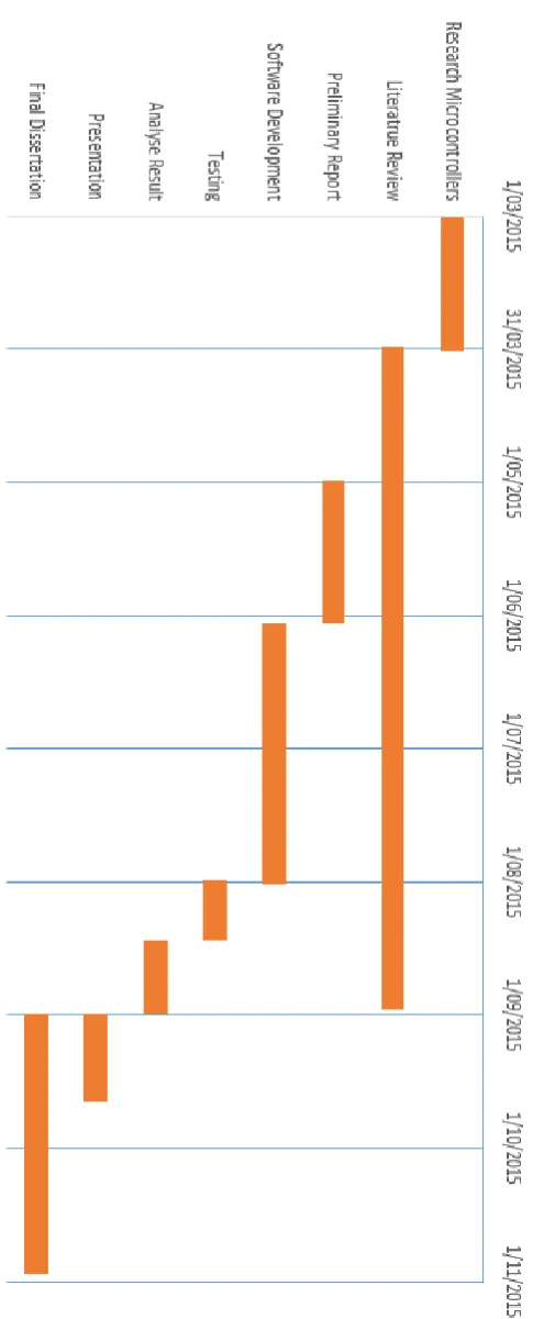
Project Timeline
Software Development
This chapter will outline the stages undertaken during the software development. This will include the software optimisation techniques as well as the process of accessing the separate hardware units contained on the development board through the software. Software libraries which have been accessed to assist with software development and image processing will also be reviewed.
The process of development of each program will be examined including the output which was required from the two machine vision algorithms. Samples of code have been included to assist with understanding of each program.
4.1 Optimisation Techniques
The literature review identified the following software optimisation techniques as being appropriate techniques to reduce execution time within software programs.
1. Loop unrolling 2. Loop reversal 3. Pointers
To test which software techniques will improve execution time the code was written and tested for two machine vision algorithms as follows:
1. Without any optimisation 2. Loop Reversal
3. Containing one loop unrolled.
4. Optimised through the use of pointers 5. Optimised with pointers and loop reversal. 6. Optimised with pointers and a loop unrolled.
7. Any calculations which can be manually vectorised to be calculated by the Neon data engine
4.2
Image Processing
Image processing was required for both programs and was achieved through the use of the following libraries.
- OpenCV - was used to import image pixel values allowing alterations to images to be made as required as well as other functions such as displaying and saving altered images. OpenCV was also used to assist with timing of execution through the getTickCount() and getTickFrequency() functions.
- OpenCL has been used to access the Graphics processing unit for the execution of kernels.
- Neon Intrinsic library was used to develop program which required access to the Neon data engine.
4.3
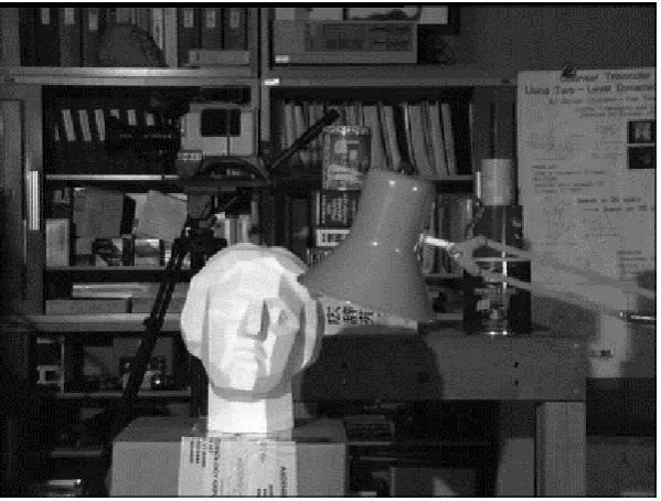
Grey Scale ThresholdingThe photo chosen to be used when testing the two machine vision algorithms was found within the sample codes in the openCV library. This image was chosen as it was a greyscale image and appropriate for testing of the programs.
Figure 4.1 (a) Input image 4.1 (b) Output image
For the purpose of this dissertation a threshold value of 128 was chosen and any value below this threshold was changed to an intensity of 0. The result of this change is shown in figure 4.1.
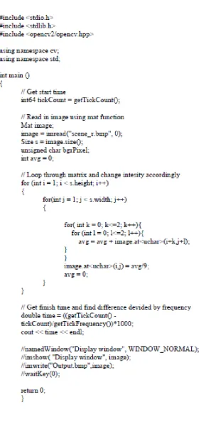
The first program to be developed was the grey scale threshold program containing no optimisations. The program was developed to loop through each pixel value in the image and change any values below the threshold. The OpenCV data type Mat was used to hold the data values of the image and the image was imported via the imread function. The Mat data type is a matrix, and as the image used was a greyscale image the matrix stored the intensity values of each pixel ranging from 0 to 255.
The second program developed and tested is the Grey Scale threshold with loop reversal. Developing this program only required a small change from the original, which included changing the loops to decrementing in place of incrementing loops. This is shown in figure 4.3 and a copy of the full program can be found in Appendix B.2.
Figure 4.3 Loop reversal for greyscale threshold.
Figure 4.4 Loop unrolling excerpt.
Figure 4.5 For loop within the Grey scale threshold algorithm with use of pointer.
The pointer optimised program was then changed to allow for loop reversal and loop unrolling and each program individually tested.
The next section of the software development comprised altering the program to allow control over which hardware units were to process the data.
The first changes made to the code was achieved by adding to the Grey scale algorithm with the use of pointers the code shown in figure 4.6.
Figure 4.6 Block of code directing process through single core
A7 Core 1 = 0 A15 Core 1 = 4 A7 Core 2 = 1 A15 Core 2 = 5
A7 Core 3 = 2 A15 Core 3 = 6 A7 Core 4 = 3 A15 Core 4 = 7
The addition of the block of code to the next two programs to be tested allowed the data to be directed through a single A7 core by setting the CPU to 0 and through a single A15 core by setting the CPU to 7. These two programs can be found in Appendix B.7 and B.8.
The next program to be developed was a Grey scale threshold program which was to be directed through the Neon data engine. As explained previously in chapter 2 section 2.2.1. The Neon data engine works with SIMD or single input multiple data stream and the software was written using neon intrinsic functions and data types. The arm_neon.h header was added to allow use of the neon intrinsic functions.
To use the neon data engine the program needed to be vectorised. Vectorisation was achieved through the use of vector data types available within the neon intrinsic library. The image pointer was declared as vector type unin8x16_t. This contains 16, 8 bit unsigned intergers. To use the neon data engine a new image was created and another pointer allocated for the altered output image data.
vector was loaded with the threshold value of 128 into each slot of the vector. This was done using the vdupq_n_u8(128).
The mask vector was used for the output of the compare of the ptr and threshold. If the ptr was greater than the threshold a value of 1 is recorded in the mask and if it is less a value of 0 is saved in the mask. An and operation is then performed on the ptr and mask and the result is then pointed to by the output image pointer. These calculations were done in a loop to ensure each pixel in the image was compared with the threshold and recorded. Figure 4.7 has an excerpt of the program containing the loop and the full program can be found in appendix B.9.
Figure 4.7 Loop for Neon data engine
The last program to be developed for the greyscale thresholding algorithm was to direct the processing through the graphics processing unit. To access the graphics processing unit OpenCL libraries where needed alongside OpenCV.
#include <opencv2/opencv.hpp> was added to allow access to OpenCV functions and the Tick count functions were added to enable timing in .line with previous programs. The original program continued, initialising variables and setting up the OpenCL environment including creating context, command queue, program and kernel.
A pointer to the input image was then initialised and the height and width of the image found. As the program was set up to take an RGB or Red Green Blue image the greyscale image was converted to RGB with the code block contained in figure 4.8.
Figure 4.8 Convert greyscale image to RGB code
A 2D Image is now created and held in memory alongside a memory object for the new output image to be written to. The image is then transferred to a RGBA format which essentially adds an extra empty container in the RGB array.
4.4
Average Smoothing Filter
The Average smoothing filter is a typical machine vision algorithm which smoothes sharp edges in images. This is calculated by adding neighbouring pixel values and replacing the pixel value with the average of these neighbours. This is demonstrated in figure 4.9. This calculation is carried out on each pixel in the image. There are issues with this type of algorithm when considering outside pixels and therefore edges of the diagram have the same value then prior to the image processing.
Figure 4.9 smoothing filter algorithm.
Figure 4.10 Original image used for image processing
Figure 4.11 Image after alterations from average smoothing filter
[image:68.595.143.454.348.583.2]The main algorithm for this program contains four loops, the first two loops are identical to the greyscale image and allow the program to loop through the width, times the height of the image. The inner two loops allow the program to find the sum of the values of the 3x3 matrix required to find the pixels average of the neighbouring values. This process continues through every pixel in the image and changes values of pixels accordingly.
The next two programs developed for the smoothing filter has the same changes that where made previously to the greyscale threshold programs. The first change being Loop reversal and as done previously this involves changing the loops to a decrement replacing the incrementing loop. A full copy of the average smoothing filter with loop reversal can be found in appendix C.2.
Figure 4.13 Loop for average smoothing filter with loop unrolling
The next software optimisation to be added to the smoothing filter is the use of pointers. This has again been achieved through the use of the IplImage data structure allowing a pointer to be pointed to the image data. The full code can be found at appendix C.4.
The pointer optimisation smoothing filter code has then had loop reversal added and as with the greyscale threshold involves decrementing loops. The full code for this software development can be found in Appendix C.5.
To direct the processing through selected cores in both the A7 and A15 processes the sched_setaffinity() function has been used as was done in the grey scale threshold and CPU values set accordingly. This has been used to direct data through an individual A7 and A15 core.
Until this point all the changes made to the original smoothing filter program have been very similar to the changes made in the grey scale thresholding programs, however the next changes were to allow the data to be vectorised and sent through the data engine unit and have very different changes. As this algorithm requires 3x3 matrix values, this has been a challenge to vectorise. The neon data engine allows a 128 bit wide vector length and this was found to be difficult to use when trying to split data into a 3x3 matrix. The pointers to the image where stored in uint8x8_t data types which only allows one value at a time. As we are now taking image data and creating a new image opposed to changing values in the original image, the outside values of the image need to be set to the original values.
Figure 4.14 Load and sum functions in average smoothing filter directed through neon data
engine.
The program adds the first three values together contained in the sum variable and divides the total by 9. This value is now stored into the output pointer, and the output pointer is incremented. This continues six times which does cause the last value in the vector to remain empty. The program continues to loop through these calculations and each time increments the ptr by a value of six. This program will only work for an image which has a width which is divisible by 6. The full code for this program can be found in Appendix C.9. The last program written for this dissertation was the average smoothing filter which was directed through the graphics processing unit. As with the grey scale thresholding algorithm a sample program was chosen which had similar requirements to the average smoothing filter. The program chose was the fir_float.cpp and kernel.
Four values from the first line of the image are loaded into a float4 vector structure through the vload4 instruction. The next container has the four values loaded from one point forward and the last container has another four values loaded from the next point forward. This would give the following values where the values contained in the data vectors are the position of the first line in the image data.
data 0 = 0,1,2,3
data 1 = 1,2,3,4 data 2 = 2,3,4,5
4.5
Testing
The calculation of execution time was found with the use of the OpenCV function getTickCount(). GetTickCount returns the number of ticks after an event (OpenCV 2014). This function were placed at the beginning of the program and again at the end. The tick count from the beginning of the program was subtracted from the end count which gave an overall tick count for the execution of the program. To turn the tick count into time the getTickFrequency() function was used. The getTickFrequency() fuction returned the number of ticks per second (OpenCV 2014). The overall tick count was then divided by the tick frequency to obtain the time in seconds and multiplied by 1000 to obtain the time in milliseconds. The code used to calculate execution time is in figure 4.1.
Figure 4.15 Copy of program section which calculates execution time.
To assist with getting an accurate representation of execution time 10 results were taken and the average used as the result.
Results and Discussion
This chapter will display and discuss test results from the execution of the developed programs. When programs were tested they were executed ten times and the average was calculated and used as the final result. All ten test results for each program have been displayed throughout this chapter. All output images from testing both the greyscale thresholding programs and the average smoothing filter programs can be found in appendix D and appendix E.
5.1
Grey Scale Thresholding
Figure 5.1 and 5.2 is an example of the effects of the greyscale thresholding image processing.
Figure 5.2 Output image from Grey Scale Thresholding
5.1.1
Results
No Optimisation
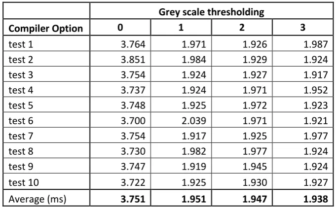
The first program tested was the grey scale thresholding program which contained no optimisations and would be used as a base time for all other tests to be compared. As seen in table 5.1 the compiler optimisations made a difference to the execution time and it can be noted that the fastest time was using the 03 compiler option.
Grey scale thresholding
Compiler Option 0 1 2 3
test 1 3.764 1.971 1.926 1.987
test 2 3.851 1.984 1.929 1.924
test 3 3.754 1.924 1.927 1.917
test 4 3.737 1.924 1.971 1.952
test 5 3.748 1.925 1.972 1.923
test 6 3.700 2.039 1.971 1.921
test 7 3.754 1.917 1.925 1.977
test 8 3.730 1.982 1.977 1.924
test 9 3.747 1.919 1.945 1.924
test 10 3.722 1.925 1.930 1.927
Average (ms) 3.751 1.951 1.947 1.938
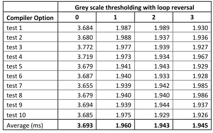
Loop Reversal
The next test performed was on the first of the optimised programs which was grey scale thresholding with loop reversal. A decrease in execution time was expected and comparing the results in table 5.2 with table 5.1 there is a small decrease in time when no compiler optimisation was chosen. When the G++ compiler is optimised using 01, 02 and 03 is used 03 is still the fastest options.
Grey scale thresholding with loop reversal Compiler Option 0 1 2 3
test 1 3.684 1.987 1.989 1.930
test 2 3.680 1.988 1.937 1.936
test 3 3.772 1.977 1.939 1.927
test 4 3.719 1.973 1.934 1.967
test 5 3.679 1.941 1.943 1.929
test 6 3.687 1.940 1.933 1.928
test 7 3.655 1.939 1.942 1.985
test 8 3.679 1.940 1.940 1.986
test 9 3.694 1.939 1.944 1.937
test 10 3.685 1.975 1.929 1.926
[image:78.595.125.468.253.467.2]Average (ms) 3.693 1.960 1.943 1.945
Table 5.2 Results from grey scale thresholding with loop reversal
Loop Unrolling
Grey scale thresholding with loop unrolling Compiler Option 0 1 2 3
test 1 4.030 2.096 2.092 2.061
test 2 3.871 2.097 2.218 2.140
test 3 3.925 2.131 2.033 2.008
test 4 3.923 2.118 2.089 2.133
test 5 3.964 2.011 2.028 2.138
test 6 4.070 2.068 2.117 2.004
test 7 4.013 2.079 2.007 2.007
test 8 4.001 2.167 2.054 2.067
test 9 4.066 2.007 2.058 2.272
test 10 4.036 2.132 2.139 2.224
[image:79.595.127.468.70.283.2]Average (ms) 3.990 2.091 2.083 2.105
Table 5.3 Results from grey scale thresholding program with loop unrolling
Pointer Optimisation
Pointer optimisation was the next optimisation technique chosen to see if the execution time can be decreased. This was the first large decrease in execution time, going from 1.938 ms to 1.201 ms using g++ compiler option 02.
Grey scale pointer optimisation Compiler Option 0 1 2 3
test 1 1.466 1.205 1.188 1.192
test 2 1.465 1.184 1.273 1.192
test 3 1.481 1.199 1.185 1.198
test 4 1.465 1.190 1.192 1.202
test 5 1.463 1.186 1.190 1.201
test 6 1.462 1.189 1.190 1.194
test 7 1.463 1.186 1.202 1.198
test 8 1.524 1.187 1.196 1.190
test 9 1.464 1.299 1.209 1.334
test 10 1.465 1.221 1.189 1.190
Average (ms) 1.472 1.205 1.201 1.209
[image:79.595.125.467.482.703.2]Pointer and Loop unrolling optimisation
Using the pointer optimisation and adding loop unrolling did not show a significant increase in code size and this is reflected in the results, however there has been a small decrease in execution time under the gcc 03 compiler option in comparison to the 03 column in table 5.4, however the result is equal to the 02 compiler option and therefore there is only an advantage using the gcc 03 compiler option.
Grey scale pointer optimisation loop unrolling Compiler Option 0 1 2 3
test 1 1.583 1.204 1.201 1.257
test 2 1.587 1.200 1.211 1.261
test 3 1.575 1.243 1.205 1.379
test 4 1.642 1.202 1.198 1.205
test 5 1.581 1.198 1.212 1.201
test 6 1.581 1.198 1.246 1.257
test 7 1.584 1.229 1.260 1.200
test 8 1.576 1.205 1.201 1.201
test 9 1.574 1.205 1.203 1.209
test 10 1.579 1.205 1.203 1.290
[image:80.595.127.466.329.537.2]Average (ms) 1.586 1.209 1.214 1.246
Table 5.5 Results from grey scale thresholding with pointer optimisation and loop unrolling
Pointer and Loop reversal Optimisation
Grey scale pointer optimisation loop reversal Compiler Option 0 1 2 3
test 1 1.462 1.256 1.219 1.231
test 2 1.468 1.260 1.222 1.223
test 3 1.507 1.274 1.221 1.230
test 4 1.498 1.282 1.223 1.228
test 5 1.469 1.225 1.277 1.361
test 6 1.467 1.222 1.229 1.230
test 7 1.460 1.265 1.225 1.231
test 8 1.515 1.235 1.224 1.227
test 9 1.472 1.222 1.223 1.227
test 10 1.495 1.224 1.263 1.236
Average (ms) 1.481 1.247 1.233 1.242
Table 5.6 Results from grey scale thresholding with pointer optimisation and loop reversal
Arm A7
The next section of testing involved using different hardware units on the development board. The first test was to use a single Arm A7 core, the results were expected to see an increase in execution time due to clock speeds in comparison to the A15. As shown in table 5.7 the expected results were seen, however this did confirm that the scheduler is processing the grey scale thresholding program on an A15 core, when it is not being manually selected.
Grey scale threshold A7
Compiler Option 0 1 2 3
test 1 4.113 2.496 2.409 2.372
test 2 4.087 2.424 2.475 2.421
test 3 4.072 2.482 2.309 2.344
test 4 4.090 2.488 2.581 2.420
test 5 4.163 2.740 2.362 2.456
test 6 3.971 2.397 2.548 2.422
test 7 4.094 2.445 2.433 2.443
test 8 4.127 2.454 2.384 2.524
test 9 4.073 2.334 2.471 2.472
test 10 4.428 2.390 2.393 2.378
[image:81.595.127.469.70.282.2]Average (ms) 4.122 2.465 2.436 2.425
Arm A15
Testing on the Arm A15 confirmed what was suspected from A7 testing results. The execution time when manually directing data through the A15 is similar to when no core is chosen, thus confirming that the scheduler is scheduling the greyscale threshold algorithm through the A15.
Grey scale threshold A15
Compiler Option 0 1 2 3
test 1 1.505 1.213 1.260 1.217
test 2 1.453 1.207 1.200 1.206
test 3 1.497 1.301 1.201 1.262
test 4 1.512 1.204 1.236 1.211
test 5 1.507 1.210 1.203 1.215
test 6 1.460 1.303 1.207 1.200
test 7 1.628 1.247 1.214 1.199
test 8 1.460 1.261 1.195 1.213
test 9 1.459 1.204 1.256 1.201
test 10 1.456 1.314 1.208 1.207
[image:82.595.129.466.246.460.2]Average (ms) 1.494 1.246 1.218 1.213
Table 5.8 Results from grey scale thresholding directed through A15 core
Neon Data Engine
Grey scale threshold Neon
Compiler Option 0 1 2 3
test 1 1.103 1.044 1.061 1.060
test 2 1.127 1.056 1.044 1.047
test 3 1.174 1.053 1.045 1.158
test 4 1.138 1.045 1.047 1.042
test 5 1.105 1.088 1.050 1.048
test 6 1.116 1.044 1.052 1.049
test 7 1.115 1.049 1.039 1.046
test 8 1.122 1.036 1.103 1.140
test 9 1.118 1.045 1.043 1.084
test 10 1.120 1.052 1.042 1.059
[image:83.595.129.466.72.281.2]Average (ms) 1.124 1.051 1.053 1.073
Table 5.9 Results from Grey Scale Thresholding directed through Neon
Graphics Processing Unit
Grey scale threshold GPU
Compiler Option 0 1 2 3
[image:84.595.130.466.72.281.2]test 1 196.482 185.425 184.421 184.108 test 2 194.219 183.977 184.450 183.520 test 3 193.843 184.489 183.435 184.147 test 4 194.104 185.935 184.185 183.828 test 5 194.005 184.838 184.066 185.166 test 6 194.750 184.106 184.765 184.584 test 7 194.073 184.656 183.670 185.410 test 8 194.753 184.122 184.443 183.809 test 9 195.198 183.789 183.692 183.447 test 10 193.974 184.939 184.289 184.055 Average (ms) 194.540 184.628 184.142 184.207
Table 5.10 Results from Grey scale program directed through GPU
Figure 5.3 contains all results from the grey scale thresholding testing.
Figure 5.3 Grey Scale Thresholding Graph
Figure 5.4 Grey Scale Thresholding Graph without GPU results
As shown in figure 5.4 the best result from making changes to the grey scale thresholding algorithm has been through the automatic compiler
5.2
Average Smoothing Filter
[image:86.595.135.461.200.449.2]The same image that was used for the greyscale filter was used again for the average smoothing filter. The output picture from the average smoothing filter is shown in figure 5.5.
Figure 5.5 Output image from average smoothing filter
The smoothing of any edges in the image can be seen, giving the image an almost blurred effect.
5.2.1
Results
No Optimisation
Smoothing Filter
Compiler Option 0 1 2 3
test 1 16.134 5.566 5.209 2.044
test 2 16.230 5.645 5.305 2.077
test 3 16.160 5.694 5.345 2.083
test 4 16.134 5.636 5.255 2.024
test 5 16.209 5.704 5.342 2.026
test 6 16.254 5.734 5.199 2.023
test 7 16.163 5.582 5.363 2.064
test 8 16.154 5.645 5.314 2.030
test 9 16.177 5.806 5.187 2.090
test 10 16.183 5.523 5.367 2.133
[image:87.595.127.466.70.289.2]Average (ms) 16.180 5.654 5.289 2.059
Table 5.11 Results from Average Smoothing Filter
Loop Reversal
The next test performed on the smoothing filter algorithm was using the software which had loop reversal optimisation added. Once again there was no advantages gained from using lop reversal.
Smoothing with Loop reversal Compiler Option 0 1 2 3
test 1 16.134 5.566 5.209 2.044
test 2 16.230 5.645 5.305 2.077
test 3 16.160 5.694 5.345 2.083
test 4 16.134 5.636 5.255 2.024
test 5 16.209 5.704 5.342 2.026
test 6 16.254 5.734 5.199 2.023
test 7 16.163 5.582 5.363 2.064
test 8 16.154 5.645 5.314 2.030
test 9 16.177 5.806 5.187 2.090
test 10 16.183 5.523 5.367 2.133
Average (ms) 16.180 5.654 5.289 2.059
[image:87.595.130.467.526.736.2]Loop unrolling
Adding Loop unrolling to the average smoothing filter has shown a large decrease in execution time when using compiler optimisation options of 0, 1 and 2. These gains were lost when compiler optimisation option 3 was tested.