ABSTRACT
SONI, PUNIT. Design and Analysis of Processor-controlled Switch Mode Power Supply (SMPS) for Embedded Systems. (Under the direction of Dr. Alexander Dean.)
c
Copyright 2011 by Punit Soni
Design and Analysis of Processor-controlled Switch Mode Power Supply (SMPS) for Embedded Systems
by Punit Soni
A thesis submitted to the Graduate Faculty of North Carolina State University
in partial fulfillment of the requirements for the Degree of
Master of Science
Computer Engineering
Raleigh, North Carolina 2011
APPROVED BY:
Dr. Greg Byrd Dr. James Tuck
DEDICATION
To my parents
BIOGRAPHY
ACKNOWLEDGEMENTS
TABLE OF CONTENTS
List of Tables . . . viii
List of Figures . . . ix
Chapter 1 Introduction . . . 1
1.1 Motivation . . . 1
1.2 Multiple voltage domains . . . 2
1.3 Dynamic Voltage and Frequency Scaling (DVFS) . . . 3
1.4 Design of a DVFS system . . . 5
1.5 Organization of this document . . . 6
Chapter 2 Related work . . . 7
2.1 Atmel AVR with integrated boost converter . . . 7
2.1.1 Boost converter operating modes in ATtiny43U . . . 8
2.1.2 Software control of boost converter in ATtiny43U . . . 9
2.1.3 Evaluation of ATtiny43U . . . 10
2.2 PSoC devices from Cypress Semiconductors . . . 10
2.2.1 PSoC architecture . . . 10
2.2.2 PowerPSoC devices . . . 12
2.2.3 Evaluation of PSoC . . . 12
2.3 Digital Power Controllers from Silicon Labs . . . 13
2.3.1 Operation of Si825x controllers . . . 13
2.3.2 Evaluation of Si825x . . . 14
Chapter 3 Design of processor controlled SMPS . . . 15
3.1 Overview of Switch Mode Power Supply (SMPS) . . . 15
3.1.1 Boost converter . . . 15
3.1.2 Boost converter operation . . . 16
3.2 SMPS design . . . 17
3.2.1 Boost converter design . . . 17
3.2.2 Choice of switching element . . . 18
3.2.3 Control signal for the boost converter . . . 19
3.2.4 Selection of the switching diode . . . 20
3.2.5 Inductor and Capacitor selection . . . 20
3.2.6 Gate driver for MOSFET . . . 21
Chapter 4 Power management in M16C/62P . . . 26
4.1 Power-saving idle modes in M16C . . . 26
4.1.1 WAIT mode . . . 26
4.1.2 Stop Mode . . . 27
4.2 Dynamic Frequency Scaling in M16C . . . 27
4.3 Implementing DFS in M16C . . . 29
4.3.1 API functions . . . 29
Chapter 5 Experimental system design . . . 31
5.1 Hardware Organization . . . 31
5.2 Power-supply control methods . . . 32
5.2.1 Feedback control of SMPS . . . 34
5.2.2 Continuous PWM mode . . . 34
5.2.3 Burst mode . . . 34
5.3 Software Design . . . 35
5.3.1 RTC Scheduler . . . 36
5.3.2 The power-supply API . . . 37
5.3.3 Tasks in the application . . . 38
5.4 Power-supply control approaches . . . 38
5.4.1 Polling based control . . . 39
5.4.2 Event based control . . . 39
Chapter 6 Results and Analysis . . . 41
6.1 Power supply efficiency . . . 41
6.2 Modes of control . . . 42
6.3 Analysis of control methods . . . 43
6.3.1 Ripple voltage measurement . . . 43
6.3.2 Computational overhead . . . 45
6.4 Experiments with dynamic frequency scaling . . . 47
Chapter 7 Conclusion and Future work . . . 51
7.1 Conclusion . . . 51
7.1.1 Design of the hardware platform . . . 51
7.1.2 Design of the software platform . . . 51
7.2 Future work . . . 52
7.2.1 Integration with a preemptive real-time kernel . . . 52
7.2.2 Integration with power-aware scheduling techniques . . . 52
7.2.3 Optimization of power supply hardware . . . 52
References . . . 54
Appendix A Interfacing peripheral devices with M16C . . . 58
A.1 TFT LCD with touchscreen interface . . . 58
A.1.1 Connecting CFA320240F-T-TS to M16C microcontroller . . 58
A.1.2 LCD display driver API . . . 58
A.2 Bluetooth modem BlueSMiRF Gold . . . 62
A.2.1 Bluetooth communication API . . . 62
A.3 SD card interface . . . 63
A.3.1 Embedded FileSystem Library (EFSL) . . . 64
LIST OF TABLES
Table 1.1 Operating voltages for various devices . . . 3
Table 4.1 QSK62P+ board current at various operating frequencies . . . 29
Table 4.2 CPU gears . . . 30
Table 5.1 Voltage domains generated by the power supply . . . 32
Table 6.1 Time taken by various control methods in 10ms duration . . . 48
Table A.1 CFA3240240F-T-TS connections in 8-bit 8080 mode . . . 60
LIST OF FIGURES
Figure 1.1 Basic blocks of a DVFS system . . . 5
Figure 2.1 ATtiny43U boost converter application circuit[20] . . . . 8
Figure 2.2 ATtiny43U boost converter efficiency vs. load current using various types of diodes[3] . . . . 9
Figure 2.3 PSoC Architecture[12] . . . . 11
Figure 2.4 Boost Converter application circuit for PSoC3 and PSoC5[13] [11] . 12 Figure 2.5 Digital SMPS controller in Si825x[14] . . . . 13
Figure 3.1 Boost converter schematic[5] . . . . 16
Figure 3.2 SMPS with feedback . . . 17
Figure 3.3 Efficiency vs. duty cycle for non-ideal boost converter[26] . . . . . 21
Figure 3.4 Gate driver using M14049 inverting buffers . . . 22
Figure 3.5 Final boost converter schematic . . . 23
Figure 3.6 LTC1442 dual comparator with in-built voltage reference . . . 23
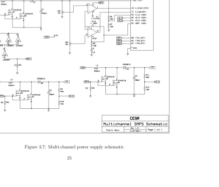
Figure 3.7 Multi-channel power supply schematic . . . 25
Figure 5.1 Hardware organization of the system . . . 33
Figure 5.2 Output voltage and control signal in burst mode . . . 35
Figure 6.1 Power supply efficiency vs load current . . . 42
Figure 6.2 Output voltage and control signal in PWM mode . . . 43
Figure 6.3 Output voltage and control signal in polling based burst mode . . 44
Figure 6.4 Output voltage and control signal in event driven burst mode . . 45
Figure 6.5 Percentage ripple in output as the polling frequency changes . . . 46
Figure 6.6 Efficiency vs polling frequency in burst mode . . . 47
Figure 6.7 Power consumption vs. operating speed in QSK62P+ . . . 48
Figure 6.8 EPC vs. operating speed in QSK62P+ . . . 50
Figure A.1 Connecting CFA320240F-T-TS to M16C microcontroller . . . 59
Figure A.2 LCD backlight connections . . . 61
Chapter 1
Introduction
Power consumption is a key issue in the design of computing systems today. While battery driven systems need to face the always increasing demand of performance with a longer battery life, the high performance systems contend with issues of heating[25]. Rapidly advancing technologies like energy scavenging, ultra-capacitor and wireless energy transmission have increased the potential market for low power, energy efficient embedded systems.
Modern embedded systems are becoming more intelligent in terms of power and energy requirements. System level software algorithms help reducing the power and energy consumption. For these algorithms to work effectively, processor requires to have a flexible control over the power supply. To develop efficient algorithms for low level real-time embedded systems, a hardware power-supply platform needs to be designed. Low level embedded systems require this platform to be flexible as well as cost effective. In this work, we have designed such low-cost power supply platform that supports three independent voltage domains. It can be controlled flexibly using an off-the shelf microcontroller. We have also designed a software API for Renesas M16C microcontroller.
1.1
Motivation
designs have reduced the energy cost of computing. The MSP430 microcontroller from Texas Instruments is based on “ultra-low-power” design that works at 0.9V and 1MHz[24].
Many low-end embedded systems do not have continuous computing needs. Power and energy can be optimized by scaling voltage and frequency according to the computing requirements. Peripherals used in the systems are also not used at all time. Having a flexible control mechanism to shutdown unused components when not needed can reduce power consumption to a greater extent. This can be achieved using a flexible and scalable power supply with multiple voltage domains.
1.2
Multiple voltage domains
Embedded systems usually have the processor interfaced with multiple peripheral devices. These devices include wireless communication links such as Bluetooth, Zigbee, Wi-Fi, GPS module, display modules such as backlit LCDs, a keypad and/or touch-screen input module, indicator LEDs, flash memory storage devices such as an SD card, audio/video interface, various analog and digital sensors including accelerometers, pressure sensors, temperature sensors, infrared sensors, ambient light sensors, compass etc. Some of these modules may or may not be included in all systems, but each modern embedded system has more than one such peripherals. Instead of using a single supply net and voltage to power the entire system, one of those sophisticated measures is to assign separate power nets to different blocks and step the voltage down wherever the performance allows. This power domain technique is commonly referred to as multi-voltage design[19].
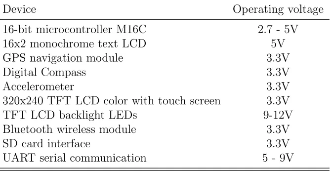
Most of the peripherals in an embedded system do not work at lower voltages as compared to the processor. For example, LCD, LEDs, flash memory. Communication interfaces such as RS-232, RF communication modules, SD cards etc. require specific operating voltages. These voltages are usually defined by the technology used in the device design. Some legacy commercial components can only operate at high voltages. Alternatively, such legacy high voltage components may be significantly cheaper than the low voltage counterparts.
Table 1.1: Operating voltages for various devices
Device Operating voltage
16-bit microcontroller M16C 2.7 - 5V
16x2 monochrome text LCD 5V
GPS navigation module 3.3V
Digital Compass 3.3V
Accelerometer 3.3V
320x240 TFT LCD color with touch screen 3.3V
TFT LCD backlight LEDs 9-12V
Bluetooth wireless module 3.3V
SD card interface 3.3V
UART serial communication 5 - 9V
potentially saved power in heat[9]. To solve this problem, an efficient power converter is
required. Switch Mode Power Supplies(SMPS) are the most commonly used and efficient solution to convert one voltage level to another. SMPS can be used to generate higher output voltages from lower input voltages. This is not possible using linear voltage regulators.
1.3
Dynamic Voltage and Frequency Scaling (DVFS)
The power consumption in semiconductor devices such as microprocessors can be divided in two parts; Dynamic power and Static power.
Ptotal =Pdynamic+Pstatic
Dynamic power results from the switching activity of the transistors. This power is dissipated in form of heat during the active processing time[22] [27]. Dynamic power is given by following equation[23].
Pdynamic=αCVdd2f
the entire semiconductor module, Vdd is the supply voltage, and f is the clock frequency. Hence, the dynamic power has a quadratic relationship with the supply voltage and linear relationship with the operating frequency.
The static power component comes from the leakage current flowing through the transistors while they are off. Static power can be approximated using following equation.
Pstatic =SpVdd2
Here, Sp is the constant with units of conductance that represents the relationship between total idle current flow and the supply voltage Vdd.
Both static and dynamic power components have quadratic relationship with the supply voltage. This leads to an obvious observation that reducing the supply voltage can help in reducing the overall power consumption. However, there is a relationship between transistor switching delay td and the operating voltage Vdd.
td∝
Vdd
Vdd−Vth
Here, Vth is the gate threshold voltage of the transistor. This delay restricts the maximum operating frequency of the processor. The relationship between the operating voltage and maximum operating frequency is;
fmax =Kp
(Vdd−Vth)2
Vdd
This equation shows that the operating frequency is limited by the available supply voltage[23]. Hence, to achieve the power savings using voltage reduction, the operating
frequency needs to be adjusted accordingly. As reducing the operating frequency lowers the computing speed, the power savings comes at the cost of reduced performance. This technique is known as Dynamic Voltage and Frequency Scaling (DVFS).
1.4
Design of a DVFS system
The basic blocks of a DVFS system are
1. Variable Speed Processor
2. Power supply capable of generating desired voltages for the processor
3. Power supply control circuit driven by the processor
4. Feedback circuit to sense the supply voltage
Figure 1.1: Basic blocks of a DVFS system
The software running on the processor senses the workload and performance require-ments. It makes decisions about the frequency scaling. The software triggers the frequency transition in the variable speed processor. At this time, a control signal is generated to signal the power supply to generate optimum voltage according to frequency. Supply voltage is monitored using feedback circuit. This makes it a closed loop control system. The processor will keep the control signal activated until the supply voltage is not in the desired range.
at more than one clock speed and the speed can be changed at run time. Usually the modern microprocessors and microcontrollers have the clock generation circuit that can be configured in software. Rest of the parts in the figure deals with dynamic voltage scaling. DVS basically needs a controllable power supply and a feedback-control mechanism. A switch mode power supply (SMPS) is used in DVS system to generate the supply voltage. We have used M16C microcontroller to implement a DVFS system. This microcon-troller has a in-built clock generation circuit that supports 8 different operating speeds. The power-supply designed to power the MCU is voltage-scalable. The PWM control signal from the MCU controls the power supply to generated desired voltage. An API has been designed to make use of this technique in various applications.
1.5
Organization of this document
Chapter 2
Related work
We studied some of the existing solutions available in the market that support control of SMPS using a processor. First one is a low-end microcontroller with integrated boost converter that provides low-voltage operation with limited control over the output voltage. Second is a dedicated power control system designed on chip along with main application processor. It provides flexible control of SMPS using differential PWM. Third is a very flexible power controller with multiple functions and its targeted towards high-end embedded systems. We analyzed the pros and cons of these solutions in terms of flexibility, efficiency and cost-effectiveness.
2.1
Atmel AVR with integrated boost converter
TinyAVR series of microcontrollers by Atmel are low cost, low power devices. They are optimized for very low voltage operation and available in miniature packages. ATtiny43U is a 20-pin device that can be operated at voltages as low as 0.7V. This is possible because of an integrated boost converter that is supplied on chip[3].
capacitor from the VCC pin to the GND are required[20].
Figure 2.1: ATtiny43U boost converter application circuit[20]
The switching PWM signal for the boost converter is generated inside the chip. Figure 2.2 shows a graph of boost converter efficiency vs. load current when using various diodes in circuit. It shows the efficiency of the converter between 70% to 80% at load current from 5mA to 30mA[3].
2.1.1
Boost converter operating modes in ATtiny43U
The boost converter in ATtiny43U has three main modes of operation; Stop, Start and Active.
1. Stop Mode Converter enters the stop mode when the battery voltage VBAT is less than minimum starting voltage for the converter; VSTART. Stop mode can also be triggered by software instruction. In this mode, the boost converter is not operating and consumes minimum current.
Figure 2.2: ATtiny43U boost converter efficiency vs. load current using various types of diodes[3]
the inductor current using high frequency 50% duty cycle control signal to raise the output voltage as quickly as possible.
3. Active Mode When both battery voltage VBAT and output voltage VCC are sufficiently high (more than VSTART and VBOOST respectively), the boost con-verter operates in active regulated mode. In this mode the boost concon-verter keeps the output voltage regulated using PWM control. Software can configure the boost converter to bypass PWM control and run at full duty cycle all time for a faster response time.
2.1.2
Software control of boost converter in ATtiny43U
In ATtiny43U, the boost converter is an independent hardware module that does not require any software interaction to operate. Although, some features of the boost converter are configurable using software. Basically, the software can select the operating mode of boost converter among Stop mode, Active regulated mode or Active full duty cycle (FDC) mode. The battery voltage can be monitored by connecting it to the on-chip ADC
2.1.3
Evaluation of ATtiny43U
ATtiny43U provides a low cost and low power design option for certain applications which require moderate performance. The downside of this option is the lack of flexibility and software control over the operating voltage. This makes it impossible to achieve dynamic voltage scaling using on-chip converter. Also, this system does not provide any support for multiple voltage domains. Hence, the boost converter can only be used to power the microcontroller. So, another power supply mechanism is necessary for peripheral devices.
2.2
PSoC devices from Cypress Semiconductors
This is an example of a more robust and sophisticated solution for low-power embedded system design. PSoC stands for Programmable System on Chip. Cypress provides three varieties of PSoC products; PSoC1, PSoC3 and PSoC5.
2.2.1
PSoC architecture
The PSoC architecture consists of a CPU subsystem with integrated SRAM, flash and EEPROM. Along with this it contains various digital and analog “building blocks” like ADCs, PWM channels, DACs, UARTs, I2C controller, USB module, analog filters, Op-amps, comparators, precision voltage references, mixers etc. PSoC also contains a programmable routing and interconnect fabric to route signals among various blocks and port pins. It enables the system designer to utilize the blocks more efficiently and select functions of port pins. The PSoC1 family devices have M8C based 8-bit microcontroller core(4 MIPS) for low end applications. The PSoC3 family devices have 8051 based 8 or 16 bit core(33 MIPS) for mid-range applications. The PSoC5 family devices have 32 bit ARM Cortex M3 CPU (100 MIPS) for high-end applications. Figure 2.3 shows the overview of the architecture of PSoC devices.
Figure 2.3: PSoC Architecture[12]
Figure 2.4: Boost Converter application circuit for PSoC3 and PSoC5[13] [11]
2.2.2
PowerPSoC devices
One other device in PSoC family is PowerPSoC. The PowerPSoC is an embedded power controller that builds up on M8C based PSoC1 devices. It is used in switch mode high power applications such as high brightness LEDs and other lighting applications. It contains four PWM controller channels. Each channel provides closed loop hysteric control with PWM output to drive an on-chip power FET capable of driving 1A at 32V. The control limits can be programmed using two DACs.
2.2.3
Evaluation of PSoC
PSoC5 chips cost from $15 to $30.
2.3
Digital Power Controllers from Silicon Labs
The Si825x series of devices from Silicon Labs are dedicated control devices used for sophisticated digital power control. This is the most flexible solution that targets high performance embedded applications with significant load current transients[24]. It provides a digital solution using DSP filter engine and fast ADC to accurately control the SMPS output using multi-phase DPWM. This eliminates the need for an analog error amplifier.
Figure 2.5: Digital SMPS controller in Si825x[14]
2.3.1
Operation of Si825x controllers
the filter is a digital code that represents the compensated duty cycle ratio u(n). The digital PWM generator (DPWM) directly varies the output timing the external power-supply gate drivers based on the value of u(n) until the difference between the VSENSE and VREF is zero. This entire digital control loop has an update rate of 10MHz[14].
Sensing circuit inside the power supply stages (current transformer, sense amplifier etc.) can provide a signal representative of inductor or transformer current. This signal connects to the pulse-by-pulse current-limiting hardware in the Si825x to the IPK input pin. This current-limiting circuitry is similar to that found in a voltage mode analog PWM. It contains a fast analog comparator and a programmable leading-edge blanking circuit to prevent unwanted tripping of the current-sensing circuitry on the leading edge of the current pulse. The threshold for the current limiting circuit can be digitally programmed. Current limiting occurs when the sensed current exceeds the programmed threshold. When this occurs, the ongoing active portions of the PWM outputs are terminated. A programmable OCP counter keeps track of the number of consecutive current limit cycles and automatically shuts the supply down when the accumulated number of limit cycles exceeds the programmed maximum. This mechanism provides a very fast over-current protection[14].
Along with this dedicated power controller, the Si825x contains an 8051 compatible 50MIPS core with RAM, flash ROM and common microcontroller peripherals. For high performance applications, this microcontroller can be used as a communication medium between the main application processor and the digital power controller.
2.3.2
Evaluation of Si825x
Chapter 3
Design of processor controlled SMPS
3.1
Overview of Switch Mode Power Supply (SMPS)
SMPS is an efficient solution for providing power to various battery operated systems. SMPS uses a switching element working at high frequency to provide the power to the load. Using switching topologies battery voltage can be scaled to other higher or lower load voltages in an efficient manner. Other solution being a linear regulator incurs waste of power due to heat dissipation[9]. Following are various DC power-supply topologies of
SMPS.
1. Boost Converterfor low voltage to high voltage conversion 2. Buck Converter for high voltage to low voltage conversion
3. Split-Pi or buck-boost converter input can be converted to lower or higher output voltage
In our discussion, we will look at boost converter topology only. The boost converter converts a lower input voltage level to a higher output voltage. Along with conversion, the SMPS in boost mode also regulates the output voltage. So, if required, an AC input can also be used[5].
3.1.1
Boost converter
Figure 3.1: Boost converter schematic[5]
transistors. Transistor used in boost converter can be a BJT, MOSFET or IGBT. Figure 3.1 shows the asynchronous mode boost converter. Switching element S is a transistor that is switched by the signal generated by a control circuit. The control signal is a pulse signal sometimes with a varying duty cycle; i/e. PWM. The element R in the figure 3.1 represents the load.
3.1.2
Boost converter operation
During the on-cycle of control signal the switch S remains closed and during off-cycle, switch becomes open. When the switch S is closed, current flows through the inductor L and builds up the magnetic field and EMF inside the inductor. During this time the diode remains in reverse bias (off). When the switch is closed, the diode becomes forward biased and current flows through it. This builds up charge in capacitor. Capacitor gets charged at voltage equal to the sum of input voltage and the EMF. The capacitor provides the power at higher voltage to the load. The frequency and duty cycle of the control signal is maintained such that, before the capacitor gets discharged, the next on-cycle charges it up. The capacitor also acts as a filter for the voltage that is supplied to the load. This kind of operation of boost converter is called Continuous mode operation.
again. This mode has two advantages. First, this mode is energy efficient as the input (battery) current flows for a limited amount of time (burst). Second, when control signal is turned off, the power supply does not generate any switching noise. This noise-free time period can be utilized for some noise-sensitive tasks by the system[30].
Figure 3.2: SMPS with feedback
To generate the desired control signal, a feedback mechanism is implemented. The feedback circuit senses the output voltage and the control circuit generates the control signal for the switch. The feedback circuit can be implemented using comparators or analog to digital converters. The control circuit can be implemented as a dedicated hardware or using a processor that runs the control logic in software.
3.2
SMPS design
In this work, our goal is to design a low cost multi-channel power supply with three independent voltage domains. This power supply should work at input voltage of 3V. All three channels of the power-supply should have independent feedback and control circuits. These channels should be controlled using logic level PWM signal provided from the microcontroller.
3.2.1
Boost converter design
• What switching frequency to use?
• Constant duty cycle or PWM?
• Synchronous or asynchronous switching mode?
• BJT or MOSFET as switching element?
• Schottky or normal switching diode?
• Value and type of the inductor?
• Value and type of the filter capacitor?
All of these design considerations affect the efficiency of the boost converter and hence the power efficiency of the overall system.
3.2.2
Choice of switching element
BJT (bipolar junction transistor) and MOSFET (Metal Oxide Semiconductor Field Effect transistor) are two design choices for boost converter switching element. The BJT is a current controlled device. The switching state (on/off) is determined by the input switching current to the base of the BJT. MOSFET is a voltage controlled device. The switching state of the MOSFET depends on the input voltage applied at the gate of the MOSFET. We decided to use a MOSFET over BJT for this project due to following reasons. MOSFETs are thermally stable and have better switching bandwidth. It is intuitive to use voltage to trigger switches in digital circuits rather than current. The MOSFET driver circuits are easily available, simple and take less power compared to BJT driver circuits.
There are choices available among various MOSFETs. The requirements are following. In this project, the battery voltage available is 3V. Also the M16C microcontroller operates under 3.3V. So, the MOSFET required being switchable at sub-TTL threshold voltages. In this category, I considered two MOSFETs for testing; BS170 and ZVN4210. BS170 had gate threshold voltage in the range of 0.8V to 3V[7]. For ZVN4210, the gate threshold
voltage is in the range of 0.8V to 2.4V[15]. The efficiency of the boost converter with
ZVN4210 can drive more drain current at gate voltage of 2.5V. High current capacity is required to switch the inductor current to ground when the switch is ON. Hence, ZVN4210 turned out to be a reasonable choice.
3.2.3
Control signal for the boost converter
An oscillator circuit is required to generate the control signal for the boost converter. There are many design options about the oscillator that can generate the switching signal for the MOSFET of boost converter. We examined following four options for this project.
1. LT1303 oscillator and feedback IC This IC includes the oscillator the feedback circuit required for a switching voltage regulator. However, this IC increases the cost of the system and does not provide the required flexibility in terms of oscillator frequency, duty cycle and the feedback output. Also, it provides less control options for the output voltage.
2. Op-Amp in comparator modeAnother option is to use an operational amplifier in comparator mode to generate oscillations for the control signal[28]. For low battery voltage based systems this option is not the best one. Op-Amp based oscillators will not work reliably at low voltages and might break the integrity of the system.
3. Astable multivibrator A simple oscillator can be built using two transistors, two capacitors and two resistors. This oscillator can be controlled using a single GPIO pin of the microcontroller. This is a robust solution even at low input voltages. This oscillator does not output PWM, and the frequency is determined by the R and C values, so it cannot be configured in software.
4. MCU timer as an oscillator M16C microcontroller has 9 hardware timers avail-able on chip. All of these timers can output a pulse to an MCU pin on overflow or underflow. Five of these timers provide PWM output[10]. The pulse-width and
In this project, we intended to explore various design options in processor controlled SMPS. Hence, the oscillator to provide control signal was chosen such that it provides maximum amount of flexibility. We decided to use the timer out signal from MCU as SMPS control signal. The timer is configured in PWM mode. The software running in the MCU can change the frequency and pulse width of the signal when required. Also, the timer output can be switch on and off by the software. This provides a flexible control of SMPS without using any extra hardware.
3.2.4
Selection of the switching diode
The output voltage of the boost converter is given by following equation[6].
Vo=
Vi−VTD 1−D −VD
Here, Vo is the output voltage, Vi is the input voltage, VT is the transistor voltage drop andVD is the diode forward voltage drop. D is the value of duty cycle of the control signal.
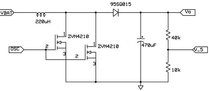
This shows that the diode voltage drop limits the value of output voltage for a given input voltage. Hence, the boost converter requires a switching diode with minimum forward voltage possible. Schottky diodes have very low forward drop voltage. In this circuit, we are using 95SQ015 Schottky diode. While a normal silicon diode have a forward voltage drop of 0.6V, the 95SQ15 has a voltage drop of 0.25V when operating at 1A[2].
3.2.5
Inductor and Capacitor selection
The inductor in an ideal boost converter has no resistance. Hence, the power loss in the ideal boost converter is zero. For a non-ideal converter the efficiency depends on many factors. One of them is the inductor resistance. In ideal converter when the duty cycle
D is zero, the voltage conversion ratio M(D) = V oV i is 1. When D approaches 1, the conversion ratio approaches infinity. However, in practical case, even with a small inductor resistance RL, M(D) approaches zero as D approaches 1. Figure 3.3 shows the efficiency of a practical boost converter with varying duty cycle. It shows the characteristic at various values inductor resistanceRL normalized by load resistanceR.
Figure 3.3: Efficiency vs. duty cycle for non-ideal boost converter[26]
generate PWM signal in discrete frequencies up to 94KHz. By experimentation, we found most efficient working of the boost converter happens at 47KHz with 220µH. The capacitor in the boost converter is used to filter the output voltage and decrease the amount of ripple present in it. We experimented certain capacitor values to find out the optimum. We used 470µF for channel 1 and 100µF for channel 2 and 3 for comparison.
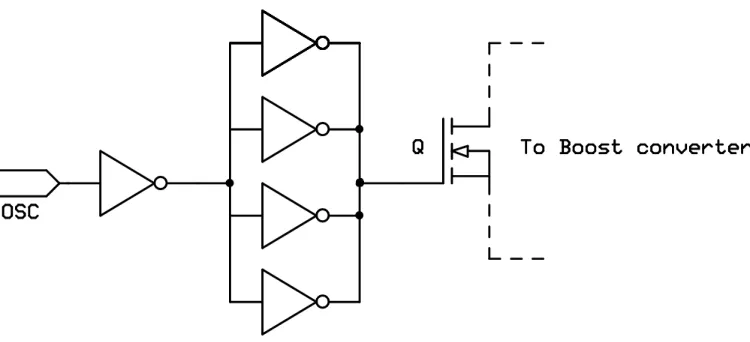
3.2.6
Gate driver for MOSFET
Figure 3.4: Gate driver using M14049 inverting buffers
using general-purpose M14049 CMOS inverting buffers. Input current of M14049 buffer is 10mA and output current is 40mA. Arrangement of the buffers shown in the figure 3.4 boosts the 10mA input signal from timer out pin to 160mA switching control signal. We incorporated this gate driver in the channel 1 of the SMPS to compare the efficiencies with channel 2 and 3 (Explained in Section 6.1).
3.3
Design of feedback circuits
Figure 3.5: Final boost converter schematic
for the divider. As the MCU VCC itself is generated by the SMPS, the ADC VREF is not constant and hence the ADC does not provide absolute reading. To overcome this problem, an external voltage reference of 1.182V is used and read using ADC. Final voltage readings are compensated in software using the constant voltage reference to generate absolute voltage values. All three channels of the SMPS are equipped with the ADC based feedback circuits.
In channel 1 of the SMPS, we added one more feedback mechanism using comparator based threshold detector. This feedback circuit is a hardware threshold detector that generates logic signals when a high or low threshold is detected. The threshold values can be adjusted using two potentiometers. For this circuit a dual-comparator IC with in-built voltage reference LTC1442 is used. This IC contains a voltage reference regulated at 1.182V[16] (this is the same voltage reference used in the ADC feedback). This reference is
Chapter 4
Power management in M16C/62P
For this project, we are using M16C/62P microcontroller from Renesas to control the multi-channel power supply. “QSK62p plus” is the development board from BNS solutions that provides interface for programming and prototyping using M16C/62P microcontroller.
In M16C, power conservation is accomplished three ways. The CPU clock can operate from the high speed or low speed crystal at various divided speeds. WAIT mode is the next feature that allows power to be conserved, while still letting the peripherals function. STOP mode is the lowest power conserving mode, drawing the least amount of current, yet allowing the device to wake up and go back to full speed.
4.1
Power-saving idle modes in M16C
The M16C microcontroller provides two idle modes; wait mode and stop mode. Wait mode stops the CPU while keeping the option of using peripheral functions open. Stop mode is more aggressive in terms of power saving as it stops all peripheral function clocks besides the CPU and brings the system to a complete halt.
4.1.1
WAIT mode
Wait mode is entered by executing the “wait” instruction in the program. The wait mode is defined as follows[10].
• CPU clock signal is stopped, hence CPU stops processing instructions
• Peripheral functions using sub-clock or external clock remain active
• System can be restored to running state by an interrupt or device reset
In this mode, the system goes in a low power state, while being able to quickly restore the previous state.
4.1.2
Stop Mode
In M16C microcontroller, stop mode implies that all the oscillations generated by clock generation circuits are stopped. Stop mode is entered by setting the “all clock stop” bit in CM1 register. The stop mode is defined as follows[10].
• CPU clock signal is stopped, hence CPU stops processing instructions
• All peripheral functions which do not use external clock are stopped
• System can be restored by a peripheral function interrupt (which use external clock), Non-Maskable Interrupt (NMI) or a device reset.
In both wait mode and stop mode, the RAM is powered and keeps the current state of the program. All the external port-pins remain at the state which was there before entering power save mode. In both modes, the interrupt used to restore the system must be setup and enabled at proper priority before entering the idle mode to make sure about the wake up.
4.2
Dynamic Frequency Scaling in M16C
The M16C CPU can be operated using one of the following clock generation circuits. These circuits also provide clock to peripheral functions; i/e. UARTs, Timers, ADC, DAC etc.
1. Main Clock
• External crystal connected at XIN and XOUT pins • QSK62P+ has a 6MHz crystal
2. On-chip oscillator clock
• 1Mhz on-chip oscillator circuit
• It is used when external oscillator is not present 3. PLL Clock
• Generated using main clock and PLL frequency multiplier • It generates 2x, 4x and 8x multiples of frequency of main clock
• M16C can be operated at maximum of 24MHz (4x mode in QSK62P+) • It can be used as CPU clock and peripheral function clock
4. Sub-clock
• Usually 32.768 kHz crystal connected at XCIN and XCOUT pins
• Can be used as CPU clock in low power mode when main clock and PLL clocks are turned off
• Sub-clock divided by 32 can be used as peripheral function clock to provide precise timings
Main clock and PLL clock generates the undivided clock frequency signal called F1. F1 is passed through a divider to generate various divided frequency signals like F2, F4, F8, F16 and F32 (F1 divided by 2, 4, 8 etc.). These signals can be used to drive CPU and/or peripheral functions.
Dynamic power consumed by the CPU depends on the operating frequency. Ability to run the CPU at lower frequency provides an opportunity to conserve power in two ways. First, the current consumed by the CPU is less when operated at lower frequency. Second, the CPU can be operated at lower voltage when it is operated at lower frequency (Dynamic Voltage Scaling). The M16C CPU provides special function registers (SFR) to control the clock generation circuit. These registers can be modified at run-time to change the CPU clock frequency. System clock control registers (CM0 to CM2) are used for this purpose.
Table 4.1: QSK62P+ board current at various operating frequencies
CPU frequency QSK board current at 3.3V
24 MHz 60mA
12 MHz 55mA
6 MHz 52.6mA
3 MHz 47.8mA
1.5 MHz 50mA
750 KHz 45.1mA 375k Hz 43.3mA 32768 Hz 44mA
4.3
Implementing DFS in M16C
Renesas provided an application note on using power saving modes and dynamic frequency scaling. Based on that idea, we developed an API to simplify the use of DFS in M16C applications. Along with the dynamic frequency scaling, this API enables the use of power saving modes in M16C with various wake-up options.
Different speeds at which the CPU can be operated are defined as gears. We have listed all possible operating frequencies for QSK62P+ in Table 4.2. The eight operating frequencies are mapped to gear 1 to gear 8. Special gear 0 is defined for the stop mode of the CPU. The API function changeGearState takes the gear number as an argument and performs the operations to put the CPU in requested gear state.
4.3.1
API functions
void initDFS() This function initializes the API global variables which are used in the other functions. It also puts the CPU in a default gear state.
Table 4.2: CPU gears
Gear Number Gear Name CPU Speed F1 Speed 0 CLK STOP 0 Hz (Stop mode) 0 Hz
1 CLK 32k 32768 Hz 0 Hz
2 CLK 375k 375 kHz 6 MHz
3 CLK 750k 750 kHz 6 MHz
4 CLK 1 5M 1.5 MHz 24 MHz
5 CLK 3M 3 MHz 24 MHz
6 CLK 6M 6 MHz 24 MHz
7 CLK 12M 12 MHz 24 MHz
8 CLK 24M 24 MHz 24 MHz
int changeGears (int gear) This function edits the SFR bit values to change the operating mode of the CPU to the requested gear state. It first determines the current CPU gear state and performs the operations (following proper order and timing requirements) depending on which state it is in right now and what state it needs to go in. If the requested gear is 0 (stop mode), this function enables a wake-up interrupt and stops all clock signals to put system in stop mode. It also saves the current system gear state in memory. The hardware interrupt is used to take the system out of stop mode. The interrupt service routine restores the saved gear state.
Chapter 5
Experimental system design
In this chapter, we’ll discuss the design of a test system used to perform experiments with the multi-channel power supply. We experimented with various methods of controlling the power-supply using a microcontroller. Quality of voltage regulation and computing overhead are the criteria for comparison among these methods. A software application using a run-to-completion (RTC) scheduler is designed. The hardware set-up of this application includes LEDs, TFT color graphic LCD with touch screen, SD card, and a Bluetooth modem. The entire system runs at 3V using two AA batteries. The multi-channel power supply produces the voltages for these devices.
5.1
Hardware Organization
Figure 5.1 shows the hardware organization of the system. The power supply generates three independent voltages from a 3V battery. Table 5.1 shows the voltage domains generated by the power supply and the devices connected to them.
Table 5.1: Voltage domains generated by the power supply
Domain Voltage Connected Devices V1 3.0V to 3.5V M16C development board V2 9V to 12V TFT LCD Backlight
V3 3.3V TFT LCD, SD Card and Bluetooth modem
from the ADC readings. Signals V1 HIGH and V1 LOW are generated using hardware threshold detector in the power supply. The threshold values are configured using the potentiometers on the power supply board. These are digital signals which are connected to M16C GPIO port pins. The details about the power supply internals and connections to M16C are shown in the schematic diagram on page 25.
This system contains three peripheral devices interfaced with the M16C development board. Here, TFT LCD is a CFA320240F-T-TS 320x240 color display with touchscreen. It is interfaced to M16C using 8-bit 8080 protocol. This display consists of a resistive touchscreen which is interfaced through ADC. Logic circuit of this display and touchscreen works at 3.3V. The backlight of this LCD display consist of four high brightness LEDs. These LEDs operate from 9V to 12V. The value of the voltage controls the brightness of the LCD display. SD card usd here is microSD from SanDisk and it is interfaced to M16C via 4-wire SPI protocol. It works at 3.3V. Third device is the Bluetooth modem BlueSMiRF Gold. It is interfaced to the M16C via UART.
All three voltage domains can generate variable voltages. Value of the voltages are controlled using the microcontroller and can be specified in software. M16C microcontroller is powered using V1 voltage from the power supply. V1 voltage is used exclusively for the microcontroller to enable Dynamic Voltage Scaling (DVS). Voltage V2 is used for the LCD backlight. Voltage V3 powers the logic circuits of LCD, SD card and the Bluetooth modem.
5.2
Power-supply control methods
Figure 5.1: Hardware organization of the system
Vo =
Vi 1−D
Here, Vo is the output voltage, Vi is the input voltage andD is the duty cycle of the control signal.
This indicates that the output voltage reaches infinity as the duty cycle reaches the value of 1. However in the real world, the switching elements of the boost converter are not ideal. The forward voltage drop across the diode VD and voltage drop across the transistor VT comes into picture. Hence, the output voltage of the boost converter can be given as,
Vo=
Vi−VTD 1−D −VD
5.2.1
Feedback control of SMPS
A feedback control system basically senses the value of the output parameter and compares to a reference to generate error signal. This error signal is used to generate the control signal for the system. In this system, we are using ADC to sense the value of the output voltage. The values read by the ADC is given to the microcontroller. The microcontroller compares the values read by the ADC to a reference value specified in the software. Based on the error value, it generates the control signal. The PWM control signal for power-supply is generated using microcontroller timer circuit. The duty cycle of the PWM control signal is modified at run-time using software.
In this system, each channel of the power-supply can be controlled in two ways. First, using continuous mode PWM signal and second, using burst mode signal with fixed duty cycle. In both modes, the value of the output voltage is read using ADC by the microcontroller. This value is compared to a reference value in specified tolerance range.
5.2.2
Continuous PWM mode
In this mode, if the value of the voltage read by the ADC is above the desired tolerance range, the microcontroller increases the duty cycle of the control signal. If the value read by the ADC is below the desired tolerance range, the microcontroller decreases the duty cycle of the control signal. So, when the value of the output voltage falls inside the desired range, the duty cycle remains stable. In a non-ideal boost converter, increasing the duty cycle after a certain maximum value, the output voltage does not increase (rather, it starts decreasing rapidly due to the power loss in the inductor, see Figure 3.3 on Page 21), so the duty cycle of the control signal is limited by a upper threshold value. In this system, if the duty cycle reaches this upper threshold value, it does not increase even if the output voltage is less than the desired voltage. In this case, the boost converter is not capable enough of supplying the desired voltage to the load.
5.2.3
Burst mode
voltage, entire control signal is switched ON or OFF. If the output voltage goes above the higher threshold value, the oscillator is turned ON and similarly if the output voltage is below the lower threshold value, the oscillator is turned OFF. In this way, the SMPS can have “blanking” intervals when it’s turned off and does not produce high frequency noise. This behavior is suitable when some devices in the system are prone to the SMPS noise. These devices can operate without problems in the blanking intervals. This technique is known as Rivalrous Hardware Scheduling[31] [30].
Figure 6.3 shows the output voltage and the control signal for a boost converter when controlled using burst mode.
Figure 5.2: Output voltage and control signal in burst mode
5.3
Software Design
non-preemptive, round-robin scheduling of the tasks.
5.3.1
RTC Scheduler
The RTC scheduler works on periodic timer ticks. The tick frequency of the scheduler can be configured. We are using 1 kHz timer frequency to have a scheduling tick every 1 ms. The scheduler uses a fixed-length task-table for keeping task data-structures. When a task is added to the scheduler, period and priority of the task is updated in the table and the task is marked as ready and enabled. The period of the task is specified in number of ticks. As this is a non-preemptive scheduler, the priority is just the number of the task which shows the fixed position of the task in the scheduling table. Each task has a unique priority value. When the scheduler starts running, it iterates through the tasks in the table and executes all ready and enabled tasks one by one. After a task is executed, the ready flag of the task is reset. The tick timer interrupt which is serviced every 1 ms, sets the ready flag of the task when the period counter of the task expires. The scheduler API is as follows.
void Init RTC Scheduler() Initializes the task data structures, scheduling timer and other data structures used by the RTC scheduler.
int Add Task(void (*task)(), int period, int priority) Adds a new task to the scheduling table. The period and priority values are updated in the data structure. If there is an existing task added to the table with same priority value, this function returns with an error code of 0 and the task is not added. On sucess the function, the function enables the newly added task, marks it ready and returns 1.
void Remove Task(void (*task)()) This function removes the specified task from the scheduling table.
void Run RTC Scheduler() This function starts the scheduling with the added tasks in the table. It iterates forever to execute all ready and enabled tasks in round-robin fashion. This function never returns.
void Reschedule Task(void (*task)(), int new period) This function is used for modifying the period of an already added task.
void Enable Task(void (*task)()) This function sets the “enabled” flag of the task specified by the function (*task)().
void Disable Task(void (*task)()) This function resets the “enabled” flag of the task specified by the function (*task)(). So, this task is not executed by the scheduler until it is enabled again.
5.3.2
The power-supply API
An API is designed to provide the interface to the multi-channel power supply. This API controls the PWM signals for each boost converter. It interfaces with the ADC to read the output voltage values. It also provides facility for the user to change the control method for a particular channel of the power supply.
void initPowerSupply() Initializes the PWM timers and interrupts. Starts all three channels with default duty-cycle values. It also initialized the ADC in repeat sweep mode for reading the voltages.
void setDutyCycle(int ch, uchar duty) This function is used to change the value of the duty-cycle of the PWM signal used to control a particular channel. Argument “ch” is the number of the channel(0, 1 or 2) and “duty” is the new value of duty cycle (from 0 to 100).
void readVoltages() Reads digital codes for voltages V1, V2, V3 and VREF from ADC and calculates actual voltage values from the code using the VREF value. It stores these values in a global array.
void setMode(int ch, int m) This function specifies the operating mode of a particular power supply channel. Argument “ch” is the channel number and “m” is the new mode value. Mode values are PWM MODE, BURST MODE, BURST MODE INT (see section 5.4.2) and OFF MODE.
int getMode(int ch) Returns the mode value of the channel specified by “ch”.
5.3.3
Tasks in the application
As described before, the application is divided into multiple tasks. Each task is a function that is called periodically by the scheduler. In this system, the control of the power supply is also implemented in a software task.
void Task updateLCD(void) This task periodically updates the LCD display.
void Task communication(void) This task is used for communication using the Bluetooth modem. It also read and writes data on the SD card.
void Task flashLED(void) This task periodically toggles an LED on the board to show that the system is working.
void Task managePowerSupply(void) This task periodically polls for the power supply voltage readings from the ADC and updates the state of the control signals for all three channels based on the mode of control for each channel. It also manages the dynamic voltage and frequency scaling (DVFS) for the system. The power-supply API provides the control over the output voltage, while the DFS API shown in chapter 4 is used for scaling the frequency of the processor. The period of the this task determines the update rate of the power-supply control loop.
5.4
Power-supply control approaches
In event based approach, the external hardware triggers an external interrupt in the processor and it is handled in an ISR(Interrupt Service Routine). Both methods have their own pros and cons. For power-supply control, we provided support for both methods in our system.
5.4.1
Polling based control
This method corresponds to the periodic “managePowerSupply” task. This task periodi-cally reads the feedback voltages for all power supply channels and updates the state of control signal depending on the mode of control(i/e. PWM mode or Burst mode). This is a total software based approach which requires minimum amount of support from the hardware. One more advantage of this approach is; the software provides flexibility of updating and modifying the control algorithms without any changes in the hardware itself. All three channels in this system support this method of control.
Along with the task based polling, we experimented with the periodic ISR based approach. In this non-preemptive scheduler the power-supply control task is prone to a deadline miss. This degrades the quality of voltage regulation. The periodic ISR works independently of the scheduler and runs the task in a timely fashion.
5.4.2
Event based control
Channel 1 in the power-supply (corresponding to voltage V1) supports an event based control using feedback signals from the hardware threshold detector. When the mode of channel 1 is set to BURST MODE INT, the logic signals generated from comparators trigger interrupts in the system. These interrupts control the channel 1 of the power supply in burst mode. Advantage of this method is; the interrupts have far better response time compared to periodic task used for the power supply. This provides better voltage regulation. Also, as this technique does not need the feedback from the ADC, it has significantly less computing overhead.
void Int2Interrupt(void) This ISR is triggered when the high threshold is detected by the hardware threshold detector in the system. The V1 HIGH signal is connected to the INT2 pin of the M16C microcontroller. It turns the control signal OFF for channel 1.
One drawback of this method in the current system is; the threshold values for the threshold detector can only be configured in the hardware using potentiometers. This limits the run-time control of the voltage by the software. This limitation can be removed by using programmable voltage divider in place of the potentiometer. In this way, the microcontroller can digitally control the values of the threshold voltages in finite number of steps.
Chapter 6
Results and Analysis
6.1
Power supply efficiency
The efficiency of all three power supply channels are determined by measuring input (inductor) current Iin and output (load) current Iout.
Pin =VinIin
Pout =VoutIout Efficiency,
η= Pout
Pin
= VoutIout
VinIin
Figure 6.1 shows the variation in efficiency of power supply channels as load current is changed. All measurements are done with Vin = 3V and Vout = 5V. All channels are regulated in PWM mode for this experiment.
In Figure 6.1, efficiency of channel 1 is better compared to the channels 2 and 3. The boost converter in channel 1 uses the gate driver circuit explained in Section 3.2.6. This circuit decreases the rise time of control signal for switching transistor in the boost converter, which in turn decreases power loss in the transistor. Rise time of the control signal without gate driver is in order of 100µs. After adding the gate driver circuit the rise time is improved to be in order of 1µs.
Figure 6.1: Power supply efficiency vs load current
6.2
Modes of control
As described in the previous chapter, the power supply in this system can be controlled in various modes. These modes either use polling based or the event driven approach. PWM MODE and BURST MODE work on polling based approach. In these modes the power supply is managed by a periodically running task. The frequency of this repeating task can be configured. We’ll call this the polling frequency. BURST MODE INT works on event based approach.
PWM MODE In this mode, each instance of the periodic task reads the voltage value from the ADC and if the values are not in the tolerance range, the duty cycle of the control signal is adjusted accordingly.
the channel is turned on or off accordingly.
BURST MODE INT If a channel is configured to work in this mode, the periodic task does not control this channel. Instead, the interrupts generated by hardware threshold detectors handle the state of the control signal.
Figure 6.2: Output voltage and control signal in PWM mode
Figure 6.2 shows the output voltage and control signal waveforms for the power supply controlled in PWM MODE. Figure 6.3 shows the waveforms for BURST MODE and Figure 6.4 show the waveforms for event based BURST MODE INT. Listing 6.1 one Page 49 shows the code for the periodic control task. Listing 6.2 one Page 50 shows the code for the event driven ISRs (Interrupt Service Routines).
6.3
Analysis of control methods
6.3.1
Ripple voltage measurement
Figure 6.3: Output voltage and control signal in polling based burst mode
The software is configured to regulate the output voltage at 5V. The load is a QSK62P+ development board running at 24MHz driving 60mA current.
Figure 6.5 shows the change in the ripple voltage of the power supply output as the polling frequency and modes of control are changed. Here, the ripple is shown as a percentage of the average DC voltage. In the polling based approach, as the polling frequency is increased, the processor works more frequently for checking and regulating the output voltage. The graph shows that the ripple behavior of the power supply is improved by increasing the polling frequency. Also, the graph shows that PWM based approach works significantly better compared to the burst mode. Also, in PWM based approach, the voltage ripple is less dependent on the polling frequency. The graph also shows the amount of voltage ripple when the power supply is controlled using hardware assisted event driven burst mode. In this mode the regulation is far better compared to the polling based approach as the response time of ISRs is better than the task response time (as explained in the next section).
Figure 6.4: Output voltage and control signal in event driven burst mode
6.3.2
Computational overhead
The computational overhead for the control of the power supply depends on the control methods. We compared various methods for controlling channel 1 of the power supply as it supports all the control methods. In polling based approach, a periodic task is repeatedly executed at a fixed frequency. While in event driven approach, the ISR is executed only when an action for the control signal is needed. So, comparing execution times of these functions directly does not make much sense. Hence, we considered a 10ms duration of operation to figure out how much time out of this 10ms is used by the CPU for power supply control. The duration 10ms is chosen as it was easy to observe these events on the oscilloscope screen with this resolution. Also, it is large enough to evaluate the computational overhead due to the power supply.
Figure 6.5: Percentage ripple in output as the polling frequency changes
is 60mA). In this case, the ISRs are executed 24 times in 10ms time duration. So, the computation time taken by the event driven method is 1.2×24 = 28.8µs. Similarly, the computation time consumed by the periodic task is 356×10 = 3560µs.
This shows a major difference in computation time when using this periodic task for power supply control compared to the event driven approach. We analyzed the reasons for this behavior. This function is using floating point multiplications and comparisons to calculate the error voltage values. As M16C microcontroller does not have a dedicated floating point unit, floating point arithmetic operations are emulated in software. This takes longer computation time. We tried to remove all floating point arithmetic from the control loop and performed the calculations using integer based fixed point arithmetic. The execution time reduced dramatically from 356µs to 20µs. So, in our 10 ms duration of interest, now this task just takes 200µs.
Figure 6.6: Efficiency vs polling frequency in burst mode
6.4
Experiments with dynamic frequency scaling
In Chapter 4, the details regarding power saving modes and dynamic frequency scaling in M16C microcontroller is explained. We measured various parameters such as total power consumption and energy per clock cycle (EPC) at various operating frequencies on QSK62P+ board. The results are based on the QSK62P+ board current values at different values of operating speeds.
Table 6.1: Time taken by various control methods in 10ms duration
Method Computation time CPU cycles % CPU time Periodic task(Floating point) 3560µs 85440 cycles 35.6% Periodic task(Fixed point) 200µs 4800 cycles 2% Event driven burst mode 28.8µs 692 cycles 0.3%
Listing 6.1: Code for the periodic control task 1 void Task_managePowerSupply()
2 {
3 int i;
4 //read voltage values from ADC channels 5 readVoltages();
6
7 //For each power supply channel... 8 for(i=0; i<3; i++){
9 if(getMode(i) == PWM_MODE){
10 if(v[i] > v_upper[i] && duty[i] > 1){
11 duty[i]--;
12 setDutyCycle(i, duty[i]);
13 }
14 if(v[i] < v_lower[i] && duty[i] < 75){
15 duty[i]++;
16 setDutyCycle(i, duty[i]);
17 }
18 }
19 else if(getMode(i) == BURST_MODE){
20 if(v[i] > v_upper[i]){
21 switch(i){
22 case 0: OSC1_RUN = 0; break;
23 case 1: OSC2_RUN = 0; break;
24 case 2: OSC3_RUN = 0; break;
25 }
26 }
27 if(v[i] < v_lower[i]){
28 switch(i){
29 case 0: OSC1_RUN = 1; break;
30 case 1: OSC2_RUN = 1; break;
31 case 2: OSC3_RUN = 1; break;
32 }
33 }
34 }
35 }
Listing 6.2: Code for the event driven ISRs 1 //NMI interrupt triggered by low-threshold detection (V1_LOW) 2 #pragma INTERRUPT NMInterrupt
3 void NMInterrupt(void) 4 {
5 if(mode[CH0] == BURST_MODE_INT)
6 OSC1_RUN = 1;
7 } 8
9 //INT2 interrupt triggered by high-threshold detection (V1_HIGH) 10 #pragma INTERRUPT INT2Interrupt
11 void INT2Interrupt(void) 12 {
13 if(mode[CH0] == BURST_MODE_INT)
14 OSC1_RUN = 0;
15 }
Chapter 7
Conclusion and Future work
7.1
Conclusion
This work aimed at building a flexible low-cost platform for efficient power management in embedded systems by having control over switch mode power supplies (SMPS).
7.1.1
Design of the hardware platform
For the flexible control and cost-effectiveness, the SMPS was designed from scratch using discrete components. This power supply provides customized control and feedback methods desirable for this project. This hardware platform is highly configurable in software. It provides the system designer to experiment with various power management algorithms and methods. Along with the power supply hardware, we assembled a useful application development platform with a graphic LCD/touchscreen, Bluetooth modem, and SD card interface. We demonstrated the use of this platform using M16C microcontroller based experimental system. This platform is actually processor independent and can be used with most of existing off-the shelf microcontrollers available in the market.
7.1.2
Design of the software platform
the operating system used. This approach can be easily integrated in real-time kernels such as MicroC-OS-II. The APIs designed for interfacing LCD, touchscreen, Bluetooth modem and SD card are also portable among various operating system environments.
7.2
Future work
This works opens doors for more research in intelligent power management for real-time embedded systems.
7.2.1
Integration with a preemptive real-time kernel
First area of work can be integration of this power supply platform in a known real-time kernel such as MicroC-OS-II. Currently, the software architecture of this system works on a non-preemptive RTC scheduler. Integration of this platform in a preemptive environment is a useful achievement. Then, it can be used along with more sophisticated real-time scheduling techniques such as EDF (Earliest Deadline First).
7.2.2
Integration with power-aware scheduling techniques
One more important area of study can be, integrating this platform into an energy scheduling mechanism such as Rivalrous Hardware Scheduling (RHS)[31]. Main objective
of RHS is to use scheduling techniques to mitigate the effect of SMPS noise on EMI sensitive components of the system. RHS implements an energy aware scheduling technique called Make And Take (MAT). In this technique, temporal and energy models of a real-time system are interleaved to control the run-times of rivalrous hardware in the system[30].
7.2.3
Optimization of power supply hardware
REFERENCES
[1] 1800r series inductor datasheet. Tech. rep., Murata Corporation. http://pdf1. alldatasheet.net/datasheet-pdf/view/276424/MURATA/18R224C.html.
[2] 95sq015 schottky rectifier datasheet. Tech. rep., Vishay Electrinics. http://www. vishay.com/docs/93419/95sq015.pdf.
[3] Attiny43u datasheet. Tech. rep., Atmel Corporation. http://www.atmel.com/dyn/ resources/prod_documents/doc8048.pdf.
[4] Bluesmirf gold documentation by sparkfun electronics. http://www.sparkfun.com/ products/582.
[5] Boost converter. http://en.wikipedia.org/wiki/Boost_converter.
[6] Boost switching converter design equations.http://www.daycounter.com/LabBook/ BoostConverter/Boost-Converter-Equations.phtml.
[7] Bs170 datasheet. Tech. rep., Fairchild Semiconductors. http://www.fairchildsemi. com/ds/BS/BS170.pdf.
[8] Cfa320240f-t-ts lcd display documentation. http://www.crystalfontz.com/ product/CFAF320240FTTS.
[9] Linear voltage regulator. http://en.wikipedia.org/wiki/Linear_regulator. [10] M16c/62p group hardware manual. Tech. rep., Renesas Electronics. www.renesas.
com.
[11] Psoc 5: Cy8c55 family datasheet. Tech. rep., Cypress Semiconductor Corporation. http://www.cypress.com/?docID=27006.
[12] Psoc technology. http://www.cypress.com/?id=2232&rID=37442.
[13] Psoc3: Cy8c34 family datasheet. Tech. rep., Cypress Semiconductor Corporation. http://www.cypress.com/?docID=29197.
[14] Si825x datasheet. Tech. rep., Silicon Labs inc. http://www.silabs.com/products/ power/PowerControllers/Pages/default.aspx.
[15] Zvn4210 datasheet. Tech. rep., Zetex Semiconductors. http://www.diodes.com/ datasheets/ZVN4210A.pdf.
[17] Dc dc converters : A primer. Tech. rep., Jaycar Electronics, 2001. http://www. jaycar.com.au/images_uploaded/dcdcconv.pdf.
[18] Introduction to smps control techniques. Tech. rep., Microchip Cor-poration, 2006. http://techtrain.microchip.com/webseminars/documents/ SMPSCntrlTechn_031809.pdf.
[19] Implementing an end-to-end low-power multi-voltage methodology. Tech. rep., Synop-sys Corporation, 2007. http://www.dianzichan.com/anonymous/ic/implement_ wp.pdf.
[20] Application note: Design guidelines for attiny43u. Tech. rep., Atmel Corporation, 2010. http://www.atmel.com/dyn/resources/prod_documents/doc8206.pdf. [21] Cpufreq subsystem. Tech. rep., Linux Kernel Documentation, 2010. http://lwn.
net/Articles/11548/.
[22] Borkar, S. Low power design challenges for the decade, 2001.
[23] Cheng, W. H. Approaches and designs of dynamic voltage and frequency scaling. Master’s thesis, University of California Davis, 2005. http://www.ece.ucdavis. edu/vcl/pubs/theses/2008-1/whcheng_thesis.pdf.
[24] Dean, A. Enabling aggressive voltage scaling for real-time embedded systems with inexpensive yet efficient power conversion. Project proposal.
[25] Dhimen, G., and Rosing, T. S. Dynamic voltage and frequecy scaling for multi-tasking systems using online learning, 2007. http://dl.acm.org/citation.cfm? id=1283825&bnc=1.
[26] Erickson, R. W. Dc-dc power converters.Wiley Encyclopedia of Electrical and Elec-tronics Engineering.http://citeseerx.ist.psu.edu/viewdoc/download?doi=10. 1.1.122.8642&rep=rep1&type=pdf.
[27] J. Rabaey, A. C., and Nikolic, B. Digital integrated circuits 2nd edition, 2002. [28] Kris, B. Intelligent smps goes digital, 2009. Article in Electron-ics technical http://www.eepublishers.co.za/images/upload/EngIT_Jan09_ ElecT_Intelligent.pdf.
[30] Sachidananda, S. Adding rivalrous hardware scheduling to the first generation freedm systems communication platform. Master’s thesis, North Carolina State Uni-versity, 2010. http://repository.lib.ncsu.edu/ir/bitstream/1840.16/582/1/ etd.pdf.
Appendix A
Interfacing peripheral devices with
M16C
A.1
TFT LCD with touchscreen interface
The TFT LCD used in this project is CFA320240F-T-TS 320x240 color display with touchscreen. It is interfaced to M16C using 8-bit 8080 protocol. This display consists of a resistive touchscreen which is interfaced through ADC.
A.1.1
Connecting CFA320240F-T-TS to M16C microcontroller
This display works on SSD2119 controller. The package contains two connectors. First is the 50-pin display connector and second is the 4-pin touchscreen connector. Figure A.1 shows the connetions between these connectors and M16C microcontroller. Display pins are connected to M16C GPIO digital ports, while the touchscreen is connected to the ADC channels of the micrcontroller. Table A.1 shows all required pin connections for using the LCD in 8 bit 8080 mode[8]. Figure A.2 shows the connection circuit for TFTLCD backlight.
A.1.2
LCD display driver API
We have written an API for M16C microcontroller from the sample code given by Crystalfontz for Atmel AVR[8]. This API is used to display graphical information on the
![Figure 2.3: PSoC Architecture[12]](https://thumb-us.123doks.com/thumbv2/123dok_us/1324385.1165330/22.612.129.505.76.441/figure-psoc-architecture.webp)
![Figure 2.4: Boost Converter application circuit for PSoC3 and PSoC5[13] [11]](https://thumb-us.123doks.com/thumbv2/123dok_us/1324385.1165330/23.612.185.417.70.254/figure-boost-converter-application-circuit-for-psoc-psoc.webp)
![Figure 2.5: Digital SMPS controller in Si825x[14]](https://thumb-us.123doks.com/thumbv2/123dok_us/1324385.1165330/24.612.105.541.262.432/figure-digital-smps-controller-in-si-x.webp)
![Figure 3.1: Boost converter schematic[5]](https://thumb-us.123doks.com/thumbv2/123dok_us/1324385.1165330/27.612.117.517.77.216/figure-boost-converter-schematic.webp)

![Figure 3.3: Efficiency vs. duty cycle for non-ideal boost converter[26]](https://thumb-us.123doks.com/thumbv2/123dok_us/1324385.1165330/32.612.141.489.72.351/figure-eciency-duty-cycle-non-ideal-boost-converter.webp)