This is a repository copy of
Simulated effect of epitaxial growth variations on THz emission
and gain of SiGe/Ge quantum cascade structures
.
White Rose Research Online URL for this paper:
http://eprints.whiterose.ac.uk/80520/
Version: Accepted Version
Proceedings Paper:
Ivanov, P, Valavanis, A, Ikonic, Z et al. (1 more author) Simulated effect of epitaxial growth
variations on THz emission and gain of SiGe/Ge quantum cascade structures. In:
UNSPECIFIED International Conference on Simulation of Semiconductor Processes and
Devices (SISPAD) 2013, 3 - 5 September 2013, Glasgow, Scotland, United Kingdom.
IEEE .
[email protected] https://eprints.whiterose.ac.uk/
Reuse
Items deposited in White Rose Research Online are protected by copyright, with all rights reserved unless indicated otherwise. They may be downloaded and/or printed for private study, or other acts as permitted by national copyright laws. The publisher or other rights holders may allow further reproduction and re-use of the full text version. This is indicated by the licence information on the White Rose Research Online record for the item.
Takedown
If you consider content in White Rose Research Online to be in breach of UK law, please notify us by
Simulated Effect of Epitaxial Growth Variations on
THz Emission of SiGe/Ge Quantum Cascade
Structures
P. Ivanov, A. Valavanis, Z. Ikonic and R.W. Kelsall
School of Electronic and Electrical Engineering University of Leeds
Leeds, LS2 9JT, United Kingdom [email protected]
Abstract—We report on the effects of growth variations on the computed electroluminescence of Ge/SiGe chirped superlattice quantum cascade structures. The chirped structures investigated comprise 50 periods, each of which has a sequence of 5-7 Ge quantum wells and SiGe barriers. We used an extended density matrix carrier transport model to calculate the electron population of each subband in a QW structure via solution of the Liouville equation. Our modelling results have shown that a 5% increase of all layers of designed structures implies 10% decrease of the electroluminescence intensity and a 15% increase implies a 40% reduction in electroluminescence. Structures with 25% increase of layer thickness lose up to 60% of their electroluminescence intensity.
Keywords—SiGe; Si-based lasers; chirped superlattice; quantum-cascade; density matrix; Liouville equation; epitaxial growth variation
I. INTRODUCTION
The modern microelectronics industry is silicon-based and thus, fabrication aspects of silicon devices are well developed and understood. Integration of electronic and optical devices requires deposition of electronic and optically active materials on the same substrate. Of particular interest is the epitaxial growth of germanium and SiGe alloys on Si substrates [1]. Quantum Cascade Lasers (QCLs) are suitable for efficient generation of radiation at terahertz frequencies. Virtually all terahertz QCLs are GaAs-based devices with maximum operating temperatures below 200K. Si has a higher thermal conductivity than GaAs and this, combined with the absence of polar optical phonon scattering in Si and Ge, imply that Ge/SiGe QCLs, if realised, would have higher operating temperatures.
One of the key issues for Ge/SiGe QCL design is that the actual thickness of epitaxially grown Ge and SiGe layers differs from the designed thickness. In conventional quantum-well (QW) laser diodes this growth error can be tolerated because their emission relies on interband transitions between states in conduction and valence bands. The energy of these transitions is typically much higher than a possible change of the transition energy due to growth errors. However the operation of QCLs relies heavily on selective injection of carriers into the lasing state, and efficient carrier extraction to
maintain a population inversion; both of which depend on precise alignment of energy levels in adjacent quantum wells which, in turn, depends on the exact layer thicknesses. Thus, the performance of QCLs is much more sensitive to growth variations.
Fig. 1 shows the thickness of epitaxially grown layers of a sample measured with Transmission Electron Microscopy (TEM) versus the designed thickness. Thicknesses of grown layers can be smaller or larger than the designed thickness. Although these growth variations are still unavoidable at present state of the art of SiGe epitaxy, they can be reduced by performing multiple calibration iterations of the epitaxial process. The calibration process is time consuming, expensive and it stops when a tolerable growth variation is reached. Having an estimated tolerable growth variation before finishing laser wafer devices helps epitaxial growth specialists to set their targets, it saves time and resources. However, the tolerable growth variations are not always known a priory, and it is difficult or impossible to estimate the tolerable variation using experimental approaches.
[image:2.595.323.540.548.671.2]In this work we report the effects of growth variations on the computed electroluminescence of Ge/SiGe chirped superlattice quantum cascade structures. Results are then used to estimate the tolerable epitaxial growth variations.
II. INVESTIGATED STRUCTURES
Ge/SiGe chirped superlattice quantum cascade structures were designed for strain-balanced growth on a relaxed SiGe buffer [1], as shown in Fig. 2. These structures were not designed to operate as QCLs, but rather optimized for a maximum electroluminescence and grown to check the precision of the SiGe epitaxial growth process.
The buffer layer itself is grown on a p-doped (100) Si substrate. The chirped structures include 50 periods, each of which has a sequence of Ge and Si0.15Ge0.85 layers. Ge layers
are the QWs and Si0.15Ge0.85 layers are the barriers for the L
valley of the conduction band.
Structures with 5 or 7 QWs are investigated in this work. An example of sequences of these structures is shown in Fig. 3. Radiative transitions in these structures appear between the upper state (8 for the 7 QW and 6 for the 5 QW structures) and the lower state, both mostly localized in the widest QW.
The thicknesses of the layers of the structures with 7 QWs per period are as follows (starting with the injection barrier): L/4.0/8.2/2.5/7.0/3.3/6.5/3.5/6.3/3.7/6.2/3.9/6.0/4.0. The main QW width is L=13, 17 and 21 nm. Bold text denotes the Si0.15Ge0.85 barriers and regular text denotes Ge wells. The
underlined text indicates doped layers with a sheet doping density of 4×1016 cm-3. The sequence of layer widths of structures with 5 QWs is L/4.0/10.6/2.8/8.2/2.9/7.4/3.0/6.4/4.0.
III. MODELLING APPROACH
The individual layer widths of these structures have been designed for the highest electroluminescence due to intersubband transitions between states localized in the widest QW, using an in-house software [2]. The software includes a self-consistent Poisson-Schrodinger solver, rate equations solver and scattering models for all relevant intersubband transitions – including electron-phonon, electron-electron, ionised impurity, alloy disorder and interface roughness scattering.
The Poisson solver uses the data stored in the material library for an initial estimation of the conduction band profiles in the individual valleys of Ge and SiGe followed by a numerical solution of the steady-state Poisson equation with cyclic boundary conditions. The solver includes the effects of space charge coming from the electron and dopant distributions. This conduction band profile is then used by the steady-state Schrodinger solver to compute wavefunctions, dipole matrix elements of transitions and state energies of a QW structure.
The scattering models allow the calculation of lifetimes that are further used in the rate equation solver to find the population of energy states of a QW structure in a steady state. The software solves the Poisson, Schrodinger and rate equations a number of times (iterations) until the population converge. Once the subband populations are known, the gain and electroluminescence spectra resulting from transitions between all pairs of states in a quantum cascade structure are calculated. Under normal conditions, seven to ten iterations are enough and calculation of all the properties of interest for the 7 QW structure takes a few minutes.
However, the conventional rate-equations based model of the quantum cascade structures neglect the coherent transport effects such as tunneling, and can predict unrealistic gain, electroluminescence and current. To avoid this problem, in this work we have used an extended density matrix carrier transport model [3] which is computationally efficient yet, in contrast to rate equation models, includes coherent coupling between states of adjacent QWs. The density matrix model calculates the electron population of each subband in a QW structure via solution of the Liouville equation using results of the in-house software mentioned above.
We assume in this work that the lattice temperature equals 4 K, the electron temperature equals 100 K, the interdiffusion length equals zero and dopants are completely ionized. The conduction band edge in the L valley of Si0.15Ge0.85 and Ge
[image:3.595.106.217.145.244.2]layers has a lower energy than in the valley and, therefore the
Fig. 2. Schematic diagram of the investigated quantum cascade Ge/SiGe chirped superlattice structure grown on inversely graded virtual substrate [1].
a)
b)
[image:3.595.88.226.418.659.2]electron population in the valley is expected to be small. Therefore, for sake of simplicity we consider L valleys only.
IV. RESULTS
A. Structures with 7 QWs per period
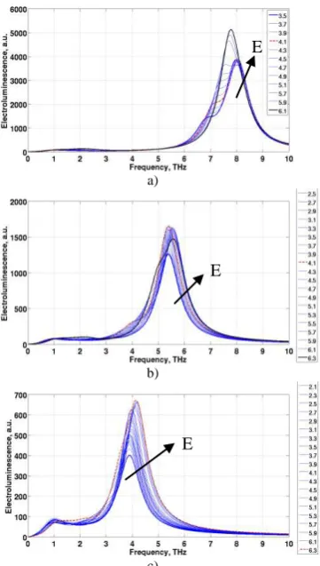
Fig. 4 shows the calculated electroluminescence spectra of structures with 7 QWs. No growth variations were introduced at this stage. These characteristics show that at low bias the structure with L=13 nm has one main emission peak at 8 THz and the secondary peak at 6.9 THz. The main emission peak originates from transitions from state 8 to state 7. The maximum of the emission appears at a bias of 4.1 kV/cm. This bias is also known as the design bias. As the bias increases, states in the structure re-align so that the secondary peak shifts towards higher frequencies, an increase of its intensity and a decrease of the emission intensity coming from the transitions between states 8 and 7.
The optimum bias of the structure with L=17 nm is 4.1 kV/cm and the structure emits at 5.3 THz. The optimum bias has not been found for the structure with L=21 nm, but these characteristics show that the structure emits at 4.1 THz
frequency. Emission peaks of structures with different L depend on the width of the main QW because the QW width is one of factors controlling the energy offsets between states of the QW.
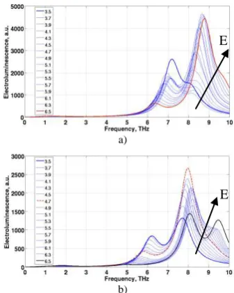
Fig. 5 shows electroluminescence spectra of these structures with the +25% increase in widths of all layers. These characteristics show that the increase of widths causes a shift of main electroluminescence peak towards smaller frequencies and a decrease of the electroluminescence intensity by up to 40%. The frequency shift is caused by a reduction of the energy spacing between states after increasing the width of QWs by 25%. The electroluminescence intensity decreases because the structure does not have the optimum alignment of states after changing the widths of layers. The frequency shift is smaller for structures with L=13 nm and larger for structures with L=21 nm. However, all the structures still do emit radiation with a large variation of layer widths introduced.
Fig. 6 shows electroluminescence spectra versus L dependence when the thickness of the main QW is increased by 5% and the thicknesses of all other layers are increased by 25%. According to these characteristics, the structure with L=13 nm will lose most of its electroluminescence. However, our results (not shown here) indicate that this structure will
a)
b)
[image:4.595.342.509.274.596.2]c)
Fig. 4. The calculated electroluminescence spectra of structures with 7 QWs at different bias values E: (a) L=13 nm (E=3.5-6.1 kV/cm), (b) L=17nm (E=1.5-6.3 kV/cm), (c) L=21 nm (E=1.1-6.1 kV/cm). No growth variations were introduced in this case.
a)
b)
c)
Fig. 5. The calculated electroluminescence spectra of structures with 7 QWs at different bias values E: (a) L=13 nm, (b) L=17nm, (c) L=21 nm. Thicknesses of all layers are increased by 25%.
E
E E
E
E
[image:4.595.75.256.288.607.2]emit in the range of biases from 3.5 to 5.1 kV/cm if the thickness of layers is increased by 15% (whilst keeping the main QW width increased by 5%). The structures with L=17 and 21 nm will emit at any bias within the investigated range with a reduced emission power.
B. Structures with 5 QWs per period
Fig. 7 shows the electroluminescence spectra of structures with 5 QWs and L=13 nm. The structure demonstrates the high-frequency dominant peak at bias exceeding 3.9 kV/cm. Growth variations have a similar effect on the characteristics of structures with L=17 and 21 nm, and these are not shown in this paper. The emission peak of structure with 13 nm wide main QW moves towards lower frequencies as the growth variation increases from 5% to 15%. When the variation is 5%, this emission still results from transitions between state 6 to states 5 or 4.When the variation is 15%, the radiation peak is caused by other low energy transitions. Thus, the structure does not operate as designed and we conclude that the variation should be below 15% if one wants the structure to operate as designed. Structures with 5 QWs have thicker layers compared to 7 QW structures and the same relative
increase of the thickness of all layers means a larger absolute increase of layer thicknesses in the 5 QW structure, hence their larger sensitivity.
V. CONCLUSIONS
The growth error of all layers in structures with 7 QWs and 5 QWs per period decreases the electroluminescence intensity. Structures with 7 QWs are able to operate as designed as long as widths of all their layers are increased up to 25%. If the variation is +25% and the variation of the main QW width is just +5%, the structure with 13 nm main QW stops operating. Other structures with 7 QWs still emit at the designed frequency. The structures with 5 QWs per period are more sensitive to growth errors and the growth error variation error for this structure should not exceed 5%.
ACKNOWLEDGMENT
This work is funded by Engineering and Physical Sciences Research Council. Authors would like to thank Dr. M. Myronov and Prof. D.R. Leadley (both from Warwick University) for providing TEM measurements used for plotting the characteristic shown in Fig. 1.
REFERENCES
[1] V.A. Shah, A. Dobbie, M. Myronov, and D.R. Leadley, “Reverse graded SiGe/Ge/Si buffers for high composition virtual substrates ,” Journal of Appl. Phys., vol. 107, p. 064304, 2010.
[2] A. Valavanis, L. Lever, C.A. Evans, Z. Ikonić, and R.W. Kelsall, “Theory and design of quantum cascade lasers in (111) n-type Si/SiGe,” Phys. Rev. B, vol. 78, p. 035420, 2008
[3] T.V. Dinh, A. Valavanis, L.J.M. Lever, Z. Ikonić, and R.W. Kelsall, “Extended density matrix model applied to silicon-based terahertz quantum cascade lasers,” Phys. Rev. B, vol. 85, p. 235427, 2012. a)
b)
[image:5.595.342.511.50.262.2]c)
Fig. 6. The calculated electroluminescence spectra of structures with 7 QWs at different bias values E: (a) L=13 nm, (b) L=17nm, (c) L=21 nm. Thicknesses of all layers are increased by 25%, the thickness of the main QW is increased by 5% compared to initial design.
a)
b)
Fig. 7. The calculated electroluminescence spectra of structures with 5 QWs at different bias values E: (a) thicknesses of all layers are increased by 5%, (b) 15%. L=13 nm.
E E
E
E
[image:5.595.76.241.123.441.2]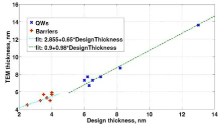
![Fig. 2. Schematic diagram of the investigated quantum cascade Ge/SiGe chirped superlattice structure grown on inversely graded virtual substrate [1]](https://thumb-us.123doks.com/thumbv2/123dok_us/8098928.233705/3.595.88.226.418.659/schematic-investigated-chirped-superlattice-structure-inversely-virtual-substrate.webp)