Rochester Institute of Technology
RIT Scholar Works
Theses Thesis/Dissertation Collections
11-2017
A Scalable & Energy Efficient Graphene-Based
Interconnection Framework for Intra and
Inter-Chip Wireless Communication in Terahertz Band
Sagar Saxena
Follow this and additional works at:https://scholarworks.rit.edu/theses
This Thesis is brought to you for free and open access by the Thesis/Dissertation Collections at RIT Scholar Works. It has been accepted for inclusion in Theses by an authorized administrator of RIT Scholar Works. For more information, please [email protected].
Recommended Citation
A Scalable & Energy Efficient Graphene-Based Interconnection
Framework for Intra and Inter-Chip Wireless Communication in
Terahertz Band
by
Sagar Saxena
A Thesis Submitted in Partial Fulfillment of the Requirements for the Degree of Master of Science in Computer Engineering
Supervised by
Dr. Amlan Ganguly
Department of Computer Engineering Kate Gleason College of Engineering
Rochester Institute of Technology Rochester, NY
November 2017
Approved By:
_____________________________________________________________________________
Dr. Amlan Ganguly
Primary Advisor – R.I.T. Dept. of Computer Engineering
_____________________________________________________________________________
Dr. Sonia Lopez Alarcon
Secondary Advisor – R.I.T. Dept. of Computer Engineering
_____________________________________________________________________________
Dr. Andres Kwasinski
ii
Dedication
I would like to dedicate this thesis to my parents Mr. Amresh Saxena and Mrs. Alka Saxena who
have supported me from the beginning of my lifetime and my mentor and friends who have
iii
Acknowledgements
I take this opportunity to express my profound gratitude and deep regards to my primary advisor
Dr. Amlan Ganguly for his exemplary guidance, monitoring and constant encouragement
throughout this thesis. Dr. Ganguly dedicated his valuable time to review my work constantly and
provide valuable suggestions which helped in overcoming many obstacles and keeping the work
on the right track. I would also like to express my deepest gratitude to Dr. Sergi Abadal for sharing
their thoughts and suggesting valuable ideas which have had significant impact on this thesis. I am
grateful for their valuable time and cooperation during the course of this work. I also take this
opportunity to thank my research group member Deekshith Shenoy Manur for all the constant
iv
Abstract
As the technology downscaling allows the integration of many cores in the same multicore
chips challenges faced are of delay, power requirements and chip area utilization. Multicore
processor architectures rely on complex memory systems in order to provide fast and efficient
means for data access and sharing between cores. Several on-chip networks have been proposed
to improve the communication efficiency of multicore system. As the number of cores on a chip
increases, the performance is limited by the communication among and within the chips.
Traditional wireline topologies become insufficient for guaranteeing desired latency conditions
without significantly affecting other metrics of throughput, bandwidth, and energy per message.
A wide range of computing hardware such as servers to embedded systems use platform based
designs with multiple multicore Systems-on-Chips (SoCs). Most computing platforms such as
embedded systems to server blades comprise of multiple Systems-on-Chips (SoCs). Traditionally,
these multichip platforms are interconnected using metal traces over a substrate such as a Printed
Circuit Board (PCB). Communications in multichip platforms involves data transfer between
internal nets and the peripheral I/O ports of the chips as well as across the PCB traces. Long
distance data communication over multi-hop wireline paths in conventional Network-on-Chips
(NoCs) cause high-energy consumption and degradation in performance. Also, the intra-chip and
inter-chip communication architectures are separately designed to maximize design flexibility.
Jointly designing them could, however, improve the communication efficiency significantly and
yield better solutions.
To satisfy the increasing demand for high speed wireless communication, many emerging
v
interconnects have been envisioned to alleviate the issues of a metal/dielectric interconnect system.
All these interconnect technologies have their own advantages along with some challenges in terms
of fabrication process or associated area overheads. In this context, disruptive solutions are
required to alleviate the limitations of Network-on-chips(NoCs) architecture in terms of latency,
providing high bandwidth and maintaining affordable power and area overheads. Current
implementations show several shortcomings related to the main enabler of wireless
communication in network-on-chips i.e. on-chip antennas. The size of future metallic on-chip
antennas, i.e. hundreds of micrometers might render unfeasible the approach of integrating at least
one antenna per core. Also, bandwidth is inversely proportional to the antenna size, metallic
antennas may not be able to provide enough bandwidth. These issues cannot be solved by further
reducing the size of a metallic antenna, as this would impose the use of very high resonant
frequencies, from the near infrared to the optical ranges.
Novel devices based on graphene structures capable of establishing wireless links are explored
in recent literature to provide high performance on-chip interconnections. Graphene-based
antennas are just a few micrometers in size, could provide intra and inter-chip communication in
the Terahertz (0.1–10 THz) band. These characteristics will both enable size compatibility with
each processor core and offer enough bandwidth. Graphene-based antennas support the
propagation of tightly confined SPP waves. Expected to be few orders of magnitude smaller than
metallic quarter wave antennas for the same resonant frequency. A few micrometer wide and long
patch antennas could effectively radiate in the Terahertz Band. Such reduced dimensions are
comparable with future core sizes, i.e. few hundreds of micrometers, enabling the integration of
one or multiple antennas per core. So, we propose that massive multicore architectures can have
vi
antenna arrays that are able to radiate signals at the Terahertz band by utilizing lower chip area
than its metallic counterparts. The employment of graphene-based antenna arrays for the design
and development of flexible and scalable interconnection framework is being proposed, as the
achieved performance capabilities and the high bandwidth with extremely low power as well as
extremely low area overhead that offered by this approach could deliver a breakthrough in massive
multicore architectures.
In this thesis, we present an innovative approach to enable THz WiNoC with low power
wireless devices operating in the THz bands such as graphene based antennas. We also propose to
extend graphene-based wireless links to enable energy-efficient, phase-based communication
protocol to create a seamless, wireless interconnection fabric for multichip systems. As compared
to the previous state of the art token based MAC protocol, the novelty of proposed phase based
communication protocol is that multiple simultaneous wireless link can be made active at a time
whereas only a single wireless link can be made active in token based system. Therefore,
performance gains for our proposed graphene based wireless system are magnificent when
compared to all other architectures compared in this paper. With cycle-accurate simulations we
show that such a design with torus like folding based on THz links instead of global wires can
outperform state-of-the-art wireline mesh and folded torus based multichip systems. We provide
estimates that they are able to provide significant gains (about 3 to 4 times better in terms of
achievable bandwidth, packet latency and average packet energy when compared to wired system)
in performance and energy efficiency in data transfer in a NoC as well as multichip system. Thus,
realization of these kind of interconnection framework that could support high data rate links in
Tera-bits-per-second that will alleviate the capacity limitations of current interconnection
vii
Table of Contents
Dedication ... ii
Acknowledgements ... iii
Abstract ... iv
Table of Contents ... vii
List of Figures ... ix
List of Tables ... x
Glossary ... xi
Chapter 1 Introduction ... 1
1.1. Network-on-Chip Paradigm ... 1
1.1.1 Network Parameters & Metrics………3
1.2. Inter & Intra-chip Communication ... 4
1.3. Emerging Multicore Integration Technology ... 5
1.4. Motivation ………...8
1.5. Research Contributions ... 9
Chapter 2 Background and Related Work ... 12
2.1. On Chip Interconnects ... 12
2.2. Emerging Multichip Integration Technologies ... 13
2.3. Graphene-Based Antennas ... 14
Chapter 3 Wireless Interconnection Framework ... 16
3.1. Topology ... 16
3.1.1 Folded Wireless Network on Chip Topology (GFWiNoC)………16
3.1.2 Multichip System Topology ... 18
viii
3.3. Wireless Communication Protocol ... 24
3.4. Flow Control and Routing ... 26
Chapter 4 Simulation Results and Analysis ... 27
4.1 Simulator Setup………..27
4.2 Energy Per bit estimation for Graphene based wireless Links………29
4.3 Optimization of Phase Duration………..31
4.4 Performance Evaluation with Synthetic Traffic……….…32
4.4.1 Peak Achievable Bandwidth per Core………34
4.4.2 Average Packet Latency……….38
4.4.3 Average Packet Energy………..…40
4.5 Performance Evaluation with Application Specific Traffic………42
4.5.1 Average Packet Latency……….43
4.5.2 Average packet Energy………..45
4.6. Comparison with All-to-All Connected Topology ………48
4.7 Area Overheads………..50
Chapter 5 Performance Evaluation with Emerging Integration Technologies……..51
Chapter 6 Conclusions & Future Work... 54
ix
List of Figures
Fig. 1: Network-on-Chip topologies ………...2
Fig. 2: Folded WiNoC architecture with wireless link deployment………..17
Fig.3: 4-chip system with wireless link deployment……….……18
Fig.4: Phase based wireless communication protocol………...24
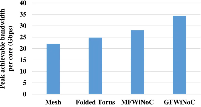
Fig.5: Peak achievable bandwidth per core as a function of phase duration……….………31
Fig.6: Peak achievable bandwidth per core of single chip architectures……….…………..35
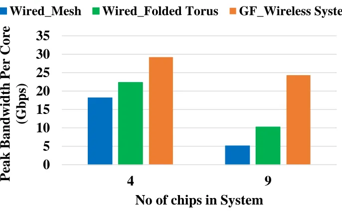
Fig.7: Peak achievable bandwidth per core of multichip system……….…..36
Fig.8: Average packet latency of various single chip architectures ………..38
Fig.9: Average packet latency for (a) 4-chip (b) 9-chip system ...………38
Fig.10: Average packet energy for single chip architectures……….………40
Fig.11: Average packet energy for multichip system.……….…...………...41
Fig.12: Percentage reduction in average packet latency w.r.t Folded Torus for application specific traffic patterns……...………....43
Fig.13: Average packet latency for application specific traffic for (a)4-chip (b)9-chip system…44 Fig.14: Average packet energy for application specific traffic for single chip ………45
Fig.15: Average packet energy for application specific traffic for (a)4-chip (b)9-chip system....47
Fig.16:Performance comparison with All-to-All Connected Topology...………...49
Fig.17: Performance evaluation of a 4-chip system with alternative technologies .……….52
x
List of Tables
Table 1: Path Loss & Energy/bit for THz band with increasing distance………....30
Table 2: Average hop-count for different architectures………..39
Table 3: Energy per bit for a single point-to-point link and possible aggregate bandwidth for
xi
Glossary
NoCs Network-on-Chips
SoCs System-on-Chips
PCB Printed Circuit Board
PCI Peripheral Component Interconnect
HPC High Performance Computing
THz Terahertz Band
SPP Surface Plasmon Polariton
CNT Carbon Nanotubes
ITRS International Technology Roadmap for Semiconductors
MAC Medium Access Unit
FDMA Frequency Division Multiple Access
SDMA Space Division Multiple Access
TDMA Time Division Multiple Access
SNR Signal to noise Ratio
OoO Out-of-order Core
WiNoC Wireless Network-on-Chip
MFWiNoC mm-Wave Wireless Network-on-Chip
GFWiNoC Graphene enabled Wireless Network-on-Chip
1
Chapter 1
Introduction
1.1
Network on Chip Paradigm
Modern day multi-processor relies on buses to share the data and allow communication to
happen between different cores on a single chip. However, with growing number of cores in
subsequent technology node the buses do not scale well, and the contention delay of the buses rises
when many or all the cores on chip request for the communication at the same time. This limitation
paved the way to development of new architectures to scale single chip multiprocessors to large
number of cores. One such method which has gained much attention in recent years is to route
processing core-to-core and core to memory traffic using an interconnection network on chip based
on routers and switches.
Network-on-Chip paradigm is an approach of designing a communication fabric between cores
of a multicore chip with an inherent property of being scalable to larger network. It is a
communication centric approach where the communication infrastructure is separated from the
functionality of the cores. It separates the communication network from the processing elements
and the data is routed over this network using intelligent switches or routers. Such an approach
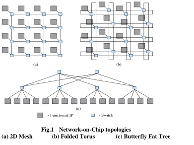
provides a scalable plug-and-play system, and facilitates reusability. Fig.1 depicts different
Network-on-Chip architecture for a 16-core system.
Network-on-Chips (NoCs) have emerged as a communication infrastructure for the multi-core
System-on-Chips (SoCs) [1]. Among different alternatives, Mesh based NoC architecture is
primarily used in multicore products [2] as it is easy to design, verify, and manufacture. Despite
2
based NoC architectures are not scalable in terms of performance and energy consumption. Folded
architectures such as Torus and Folded Torus were proposed to improve the performance of Mesh
based NoCs while retaining the regular tile-based structure for ease of manufacturing [3].
Long-range metal wires in a Mesh based NoC [4] and ultra-low-latency and low-power express channels
between communicating cores [5] have also been proposed to improve the performance of
conventional NoCs. However, the performance gain of these approaches is limited due to
metal/dielectric based interconnection. If these long-range links are realized with emerging
non-charge-transfer technologies like photonic, RF, surface-wave or wireless interconnects, the
performance and energy-efficiency of NoCs can be significantly improved [6][7][8][9]. However,
photonic and RF interconnects need the additional physically overlaid optical waveguides or
micro-strip transmission lines to enable data transmission across the NoC. On the other hand,
long-range wireless shortcuts operating in the millimeter-wave (mm-wave) do not require laying out of
physical interconnects. Using such on-chip antennas embedded in the chip wireless NoC (WiNoC)
- Functional IP - Switch
(a) (b)
(c)
Fig.1 Network-on-Chip topologies
[image:14.612.131.522.61.353.2]3
architectures have been proposed [9][10]. These architectures are shown to improve energy
efficiency and bandwidth of on-chip data communications. However, the date rate of the mm-wave
wireless channels is limited by the state-of-the-art power-efficient transceiver design.
Network-on-chips have many advantages over the conventional methods of on-chip
communication:
1) Scalability and Replicability.
2) On chip wiring resources are shared between all cores thereby improving the efficiency of
chip area used for wiring.
3) Wiring in NoCs has a more regular structure, allowing better optimization of electrical
properties that would result in less cross-talk.
4) NoCs are modular and their interfaces can be standardized.
1.1.1
Network Parameters & Metrics
Before diving into the insights about interconnection systems, it is imperative to characterize
the parameters that are utilized to define networks and the performance metrics that are used to
gauge the network performance [3].
Flits: Wormhole routing is used to improve the network performance. In this routing, individual
packets are divided in to smaller segments that are known as flits. Flit width is the number of bits
per each flit and in general is equal to the width of the physical link.
Hop Count: Movement of a flit from one router to another is defined as a single hop. Hop Count
is the total number of hops a flit makes from the source node to its destination node. Average hop
4
hop count of a network should be low as this would ensure that the flits can reach their destination
faster and hence the network if connected properly.
Network Diameter: The longest minimal hop between two communication cores in a network is
known as the network diameter.
Peak Achievable Bandwidth per Core: The peak achievable bandwidth per core is measured as
the maximum sustainable data rate in number of bits successfully routed per core per second at
network saturation.
Average Packet Latency: It is the average number of clock cycles required to transmit a packet
to the destination core successfully. Due to different average distances between cores in the
different interconnection architectures, the latency characteristics are different for every network.
Average Packet Energy: Average packet energy is the energy consumed to transfer an entire
packet from source to destination in the multichip system on average.
1.2
Intra & Inter-Chip Communication
A wide range of computing hardware such as servers to embedded systems use platform based
designs with multiple multicore Systems-on-Chips (SoCs). With the increase in computational and
functional complexity of these platforms, the number of individual SoCs or multicore chips
increases manifold [11]. This makes the interconnection in these systems grow in both size and
complexity. The performance and overall energy efficiency of these platforms therefore depend
on the performance of the interconnection architecture that is responsible for the system
integration. While intra-chip communication infrastructure is seeing a paradigm shift from
bus-based systems to Network-on-Chip (NoC) architectures [1], inter-chip communication also needs
5
thermal envelopes. Traditionally, inter-chip interconnections are realized using solder bumps or
C4 interconnects placing individual chips on a substrate or Printed Circuit Board (PCB). Other
chip-to-chip interconnects such as Peripheral Component Interconnect (PCI) is one of the most
common standard local I/O bus technology to interconnect board-level multichip systems.
Recently, PCI express (PCIe) is presented as next generation I/O technology [12].
Recent trends according to the International Technology Roadmap for Semiconductors (ITRS)
predict that the pitch of the I/O interconnects in ICs is not scaling as fast as the gate lengths or
pitch of on-chip interconnects [13]. However, the pitch and physical bandwidth density of on-chip
global interconnects are scaling relatively better with technology. This implies a gap in density
and performance of traditional I/O systems relative to on-chip interconnections. Moreover, longer
and bulkier substrate traces for inter-chip communication due to the wiring complexity further
aggravates the crosstalk and the signal integrity issues. Typically, inter-chip communication
involves multihop paths over intra-chip global wires in both source and destination chips, I/O
blocks and substrate traces. Often the intra and inter-chip communication protocols are also
different to offer design flexibility to design teams. Due to these factors the efficiency of the
multichip system in terms of bandwidth, latency and energy consumption is reduced.
1.3
Emerging Multicore Integration Technologies
Many emerging alternative interconnect solutions [14] like inter-chip photonics, vertically
integrated monolithic 3D ICs [15] or silicon interposers [16] are envisioned as solutions to the
off-chip interconnection challenges. However, the inability of the pitch scaling makes the adoption of
photonic interconnects challenging for high complexity scalable multichip systems. Similarly,
6
them infeasible for large scale adoption so far. The use of silicon-interposers which are themselves
large dies with abundant wiring resources seem to emerge as a low-cost and high-yield alternative
to photonic or monolithic 3D integration. Using the interposer multiple chips can be interconnected
using its on-die wires which can implemented in the same technology node as the chips. The chips
are typically packaged onto the interposer die using microbumps whose relatively smaller pitch
compared to C4 bumps makes the interposer outperform traditional substrate based multichip
systems [16].
On the other hand, recent research has brought to light novel graphene based antennas operating
at THz frequencies [18] [19]. Due to the higher operating frequencies compared to mm-wave
transceivers, the data rate that can be supported by these antennas are significantly higher. Using
the plasmonic resonance in graphene, these antennas are able to provide high bandwidth (in the
range of hundreds of Gbps). Moreover, higher operating frequencies imply that graphene based
antennas are just hundred micrometers in size [19] compared to dimensions in the range of a
millimeter of mm-wave antennas. Such reduced dimensions are suitable for integration of several
such transceivers in a single NoC for relatively low overheads.
Recent research envisions wireless communication in the Terahertz band (0.1-10THz) as a key
technology to satisfy the increasing demand for high speed communication in multicore chips [17].
Wireless data communication links up to several centimeters in length with graphene based
antenna arrays are demonstrated are proposed in recent literature [19]. Due to growing interest in
this communication technology, novel transmitting and receiving devices based on micro-scale
graphene structures have been investigated [19]. It is demonstrated that such graphene based
antenna structures are capable of establishing THz band wireless links which can be used for
7
developed in [20] which shows possible communication range of up to 10m. These wireless
interconnections are shown to improve energy efficiency and bandwidth of on-chip data
communication in multicore chips over state-of-the-art counterparts. In this work, we propose to
use such graphene based THz band wireless interconnects to establish a seamless communication
backbone which enables data exchange between cores in a single chip as well as between chips in
a multichip system with dimensions spanning several centimeters. High efficiencies combined
with micro-scale device geometries tuned to THz frequencies makes this graphene based
transceivers ultra-low power. Therefore, graphene based wireless interconnections can improve
the energy efficiency of multichip systems significantly.
We propose to extend the intra-chip NoC fabric across multiple chips where each chip is
potentially a multicore system or SoC [16]. The same communication protocols used for data
transfer in the intra-chip NoCs will be used for off-chip data as well, eliminating the need for
protocol transfer. Few nodes inside the chips will be equipped with graphene based wireless
transceivers, which will fold the overall extended NoC by communicating with other such nodes
across multiple chips to reduce the diameter of the interconnection fabric. Here, we exploit the
benefits of a regular NoC structure in conjunction with emerging wireless interconnect
technologies. We explore the design of a folded Wireless NoC architecture and proposes
integration of multichip systems that utilizes a novel phase based communication protocol and
demonstrate that the proposed design outperforms traditional wired I/O based multichip systems.
Through cycle-accurate system-level simulations, we demonstrate that the proposed design can
outperform wireline and wireless counterparts while reducing the energy consumption in on-chip
8
1.4
Motivation
Long distance data communication over multi-hop wireline paths in conventional
Network-on-Chips (NoCs) cause high-energy consumption and degradation in performance. Many
emerging interconnect technologies such as 3D integration, photonic, Radio Frequency (RF) and
wireless interconnects have been envisioned to alleviate the issues of a metal/dielectric
interconnect system. Most computing platforms such as embedded systems to server blades
comprise of multiple Systems-on-Chips (SoCs). Traditionally, these multichip platforms are
interconnected using metal traces over a substrate such as a Printed Circuit Board (PCB).
Communications in multichip platforms involves data transfer between internal nets and the
peripheral I/O ports of the chips as well as across the PCB traces. This multi-hop communication
leads to higher energy consumption, decrease in data bandwidth and increase in message latency.
To satisfy the increasing demand for high speed and low power interconnects, THz Wireless NoC
(WiNoC) enabled with high-speed direct links between distant cores is desired.
Novel devices based on graphene structures capable of establishing wireless links are explored
in recent literature [19] to provide high performance on-chip interconnections. Therefore, we
present an innovative approach to enable a NoC as well as multichip systems of various size with
low power wireless devices operating in the THz bands such as graphene based antennas. We
propose to extend graphene based wireless links to enable energy-efficient, phase-based
chip-to-chip communication to create a seamless, wireless interconnection fabric for multichip-to-chip systems.
With cycle accurate system-level simulations, we provide estimates that they provide significant
gains in performance and energy efficiency in on-chip & chip-to-chip data transfer in NoC based
9
1.5
Research Contributions
This thesis will explore the possibility of seamless inter and intra-chip wireless communication
in Terahertz band by making use of graphene based THz band antenna array that are able to radiate
in Terahertz band with very low power. It will be shown that wireless interconnects can be used
to establish a seamless communication infrastructure for single chip and multichip systems within
a single package by making use of graphene-based antennas. These graphene-based antennas are
two orders of magnitude less than their metallic counterparts, so they are also able to provide a
very large bandwidth as it is inversely proportional to the size of antenna. For communication to
happen in terahertz band there is a high path loss problem along with the integration of these
antennas that would be integrated with the standard CMOS process.
Current interconnection frameworks are not capable to fully exploit the true potential of this
technology. As this field has seen many advancements in research recently, this thesis will explore
the architecture and the interconnection framework for multichip communication along with a
suitable MAC Protocol that would aid to harness the advantages of using graphene based antennas
and available large bandwidth in Terahertz band. The wireless links will span distances from
20mm up to a few tens of centimeters, using the same communication protocols for both inter-chip
and intra-chip data transfer. The developed architecture would enable efficient data sharing
between cores in single chip as well as in multichip systems, thereby merging both the inter-chip
and intra-chip networks. Novel phase based communication protocol has been employed for both
inter and intra-chip data transfer. Wireless transceivers will be integrated in a select few cores in
the chips, and each of these cores will be able to communicate directly with other such cores in a
single hop, within the same or different chips. The internal cores to be equipped with the graphene
10
network diameter that would ultimately reduce the multihop communication as well as improve
the energy efficiency.
The following points will summarize the contributions made during this work.
•Proposed Interconnection Architecture
o Development of a methodology for seamless interconnection between on-chip and chip-to-chip
data transfer by employing emerging graphene based THz band antennas.
o Design of a seamless hybrid wired and wireless interconnection network for single chip as well
as 4-chip & 9-chip systems.
•Proposed Novel MAC Protocol: Phase based Communication
O Design of a novel wireless communication protocol to fully utilize the performance gain of
highly directional graphene antenna arrays and avoiding interference between wireless links.
•Wireless Link Budget Analysis forEnergy/bit estimation of Graphene-based wireless links
•Evaluation of Wireless Single chip & Multichip Architectures
o Evaluation of peak achievable bandwidth for varying system size.
o Evaluation of average packet latency & packet energy dissipation network for varying system
size with synthetic traffic.
O Analysis of packet latency and packet energy for the systems with Application specific
traffic patterns.
O Comparison of performance metrics of the proposed wireless multichip architecture with the
11
•Development of simulation framework
o Development of a cycle accurate simulator to implement the wireless multichip architecture
and monitor the progress of flits over the switches and links per cycle.
o Include the power consumption parameters of both the wired and wireless links in the simulator
to model the energy consumption in data exchange in the single as well as multichip system.
o Obtain experimental results of the single chip and wireless multichip architecture in terms of
the following metrics for performance evaluation:
▪Peak achievable bandwidth per core
▪Packet energy dissipation
12
Chapter 2 Background and Related Work
Related work has been discussed in three subsections. First subsection relates to the on chip
interconnection and networks, second subsection relates to conventional multichip integration and
emerging technologies for inter-chip communication whereas the third subsection discuss about
the potential of THz band graphene-based antennas.
2.1
On chip Interconnection
NoC have emerged as a communication infrastructure for multi-core chips. As the number of
cores increases on a single chip, interconnection of cores in such systems becomes complex.
Despite its advantages performance and overall energy efficiency of these platforms therefore
depend on the performance of the interconnection architecture that is responsible for the system
integration. Several alternative technologies exist for realizing on-chip wireless interconnections
[9][10][21][22] . Comprehensive surveys regarding various wireless NoC (WiNoC) architectures
and their design principles is presented in [22]. Transmission line based Radio Frequency (RF)
Interconnects, surface wave based communication channels are proposed in [7][23] . Energy
efficient WiNoC architecture with Zigzag antenna and millimeter wave transceivers is proposed
to design a mm-wave wireless NoC in [9][10][22]. In [21], mm-wave wireless NoC with
directional log-periodic antenna is proposed. To increase the channel bandwidth, authors [24] has
proposed an mm-wave WiNoC architecture with multiple non-overlapping channels to enable
Frequency Division Multiple Access (FDMA) based Medium Access Control (MAC) mechanism.
However, such FDMA based approach is non-trivial from the perspective of transceiver design
and the number of concurrent channels is not easily scalable. All these mm-wave WiNoC
13
bandwidth due to their size. Mm-wave antennas based on metal cannot be reduced further due to
limitations in standard CMOS lithography process. Also, bandwidth is inversely proportional to
the size of antenna. Therefore, to have much higher bandwidth, novel devices operating in THz
band which are orders of magnitude lower in size as compared to the metallic antennas are being
investigated.
2.2
Emerging Multichip Integration Technologies
According to ITRS, off-chip global wires does not scale proportionately with on-chip wires.
Traditional methods to interconnect chips in multichip systems involve C4 bumps coupled with
in-package transmission lines [13]. However, performance with transmission lines is limited by
many factors such as crosstalk coupling effects, signal reflections, signal quality deteriorations due
to microwave effects and frequency-dependent lines losses in the transmission lines. This in turn
limits the number of concurrent high density inter-chip I/O which restricts the possible off-chip
bandwidth. To further alleviate the problem of multichip integration with conventional I/O based
system many alternatives technologies such as vertically integrated 3D integration [15], silicon
interposer [16], photonic interconnects [15][14], RF interconnect [7] inductive or capacitive
coupling based interconnects [25] and wireless interconnects [26] are being explored. In 3D
stacked approach the individual dies need to be thinned to accommodate Through-Silicon-Vias
(TSVs) through it which can induce die cracking leading to yield issues and the increased power
density results in severe thermal challenges. Photonic and RF interconnects need the additional
physically overlaid optical waveguides or micro-strip transmission lines to enable data
14
On the other hand, long-range wireless shortcuts operating in the millimeter-wave (mm-wave)
or Terahertz band do not require laying out of physical interconnects. High-Performance
Computing (HPC) environment with wirelessly connected multichip module have been proposed
in [26]. In [27] transceivers for 60GHz inter and intra-chip communications are designed.
However, this work does not evaluate system-level performance. In [27] fast pre-bonding wafer
testing was enabled by using on-chip wireless transceivers that provided direct accesses to
components under test within the ICs. In [28] performance of intra and inter-chip communication
of a multichip system was evaluated using mm-wave on-chip metallic antennas. Different medium
access mechanisms ranging from simple token passing based protocol to more sophisticated
CDMA based protocol have been explored for mm-wave wireless interconnects [29][30][31]. To
exploit full potential of wireless interconnects, novel MAC protocol utilizing the full benefit of the
topology needs to be investigated. Mm-wave antennas along with token based communication
protocol have been shown to improve the performance of wireless system by enabling single
wireless link at a time. However, mm-wave metallic on-chip antennas are limited in their
bandwidth and the supported data rates are a few Gbps depending on the transceiver design.
Therefore, to improve the bandwidth further novel devices working as transceivers and antennas
such as graphene based nanostructures need to be investigated. In our work, we utilize
simultaneous wireless communication as compared to single wireless link in token based system,
which are aided by novel phase based communication protocol.
2.3 Graphene based Antennas
While metallic antennas have shown to improve the performance of wireless system,
achievements in performance gain are impressive but these gains could be huge with some other
15
predicted to provide high bandwidth wireless communication channels [18][19]. On-chip antennas
realized by graphene based structures are predicted to operate both as modulators as well as
antennas providing high bandwidth wireless communication in the THz frequency channels
[18][19]. In [32][33] authors evaluated the feasibility of a Wireless NoC (WiNoC) architecture
realized by graphene based omnidirectional antennas. However, the performance gain for such
WiNoCs are limited as only a single wireless link can be active at any given point of time due to
the omnidirectional nature of the antennas. Recently, directional array of graphene antennas has
been explored in [19]. This will enable novel architectures and communication mechanisms using
THz graphene antennas. We also propose a novel phase based communication protocol to enable
simultaneous wireless links which would improve the performance of system drastically.
Therefore, in this work, we propose a hybrid interconnection fabric for single chip & multichip
systems using both on-chip wired links for intra-chip and low power high bandwidth THz-band
16
Chapter 3 Wireless Interconnection Framework
3.1. Topology
Every core in each chip is integrated with a NoC switch, and the switches within each
independent chip are interconnected using an intra-chip NoC architecture. The system is proposed
with Mesh based intra-chip NoC topologies and their interconnection architectures are described
below:
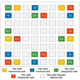
3.1.1. Folded Wireless Network on Chip Topology (GFWiNoC)
We present the design of a folded NoC architecture with wireless links in this section. The
ideal approach for folding a NoC is to connect the switches directly that are farthest away from
each other. On a planar Mesh NoC, these are the diagonally opposite switches. Interconnecting
diagonally opposite switches are challenging with wired links due to unmanageable wire delays.
Therefore, we propose to use the wireless links to enable the folding of the diagonally opposite
switches. In order to establish point-to-point links between the diagonally opposite switches we
envision the use of directional array of graphene antennas operating in the THz frequency bands.
Due to the high operating frequency, the antenna arrays are very directional and also are relatively
small in size compared to mm-wave counterparts. Therefore, in the proposed topology we place
directional antenna arrays oriented towards each other for maximum coupling. In this way, the
corners of the planar NoC are folded over resulting in 2 diagonal modes of communications as D1
and D2 in Fig. 2. In addition to the corners, we also want to enable folding of both opposite and
adjacent edges of the NoC. In order to achieve this, the selected switches along the edges are
17
and adjacent edges. Folding to connect opposite horizontal edges in Fig. 2 is achieved by deploying
the antennas in switches along those edges enabling a vertical mode of communication marked as
V. Similarly, folding to connect opposite vertical edges is achieved by deploying the antennas in
switches along those edges enabling a horizontal mode of communication marked as H. Not all
the switches along the edges are equipped with the graphene transceivers to avoid interference as
discussed later in the section 3.3 on communication mechanism. Similar to folding opposite edges,
the adjacent edges are also folded by introducing more diagonal links in both D1 and D2 modes
as shown in Fig. 2.
The graphene antenna arrays operating in the same mode (H, V, D1 or D2) communicate
concurrently in the same THz frequency band. Therefore, to avoid interference between them,
transceivers in the same mode are not deployed in adjacent switches. This avoids multiple
[image:29.612.188.452.70.334.2]transceivers being in the range of the main lobe of the radiation pattern of an antenna array.
18
Therefore, each link in the same mode can operate concurrently. The communication mechanism
to coordinate between the four modes of communication is discussed in section 3.3.
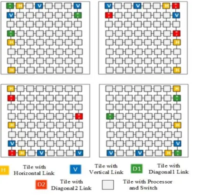
3.1.2. Multi-Chip System Topology
The proposed wireless interconnection fabric consists of multiple multicore SoCs as shown in
Fig. 3. Cores within each individual chip are interconnected by an chip NoC. While the
intra-chip NoC can be of any architecture such as regular tile-based mesh or irregular custom designs
[image:30.612.122.528.286.676.2]depending upon applications and design trade-offs, in this work the topology of the intra-chip
19
NoCs is chosen as mesh as it is a conventional NoC topology used in several multicore based
products and is relatively easy to design, verify and manufacture. To utilize the benefit of regular
NoC structure while alleviating the issues of wireline inter-chip links we equip certain NoC
switches in the multicore chips with emerging graphene based wireless transceivers. To create
these inter-chip wireless interconnects we propose a toroidal folding approach by making use of
the high bandwidth, directional point to point graphene antenna arrays that can directly connect
distant switches in the multichip system with a single hop. In a planar mesh NoC fabric is simply
extended to span multiple chips, the diagonally opposite switches will be far apart.
Multi-hop data transfer over such long-wired paths leads to unmanageable delays and energy
dissipation. To avoid these delay and energy limitations we propose a toroidal folding approach
by making use of wireless links to enable the folding of the diagonally opposite switches to reduce
the distance between communicating cores. This will lead to lower delay and lower energy
dissipation. We propose to use directional array of graphene antennas operating in the terahertz
band to enable point to point wireless links between the farthest switches of the multichip system
located along corners and edges. These arrays are shown to be highly directional [19] as discussed
later in section 3.2.
The strategy to form the multichip system interconnection fabric can be understood as same as
discussed in section 3.1.1 considering that the distant switches are now at the corners of different
chips. First, the topology is folded along the diagonals which results in 2 different diagonal modes
of communication D1 & D2 between switches at the corners of the chips as shown in Fig. 3.
Following folding the diagonally opposite corners, the opposite edges are folded by equipping
switches at the edges in each chip with the graphene array based transceivers to form the vertical
20
of adjacent edges by equipping the selected switches along the edges with graphene antenna arrays
that are directed towards each other to augment the diagonal modes of communication D1 and D2.
This is achieved by connecting the switches along the edges in addition to the corners. In this way
folding along all the 4 edges results in 4 modes of communication namely, H, V, D1 and D2.
Another advantage of using this toroidal folding based approach is that it can be scaled well
from a single chip system to a multi-chip system whose arrangement can be thought of as an array
of chips considering the intra-chip NoC to span over the array of chips where inter-chip links are
realized only with the graphene based links. In general, this folding approach can be extended for
an NxN array of chips. Only few switches amongst all in the multichip system that help in toroidal
folding the interconnection architecture have been selected and deployed with the graphene
transceivers. This deployment is done in such a way that multiple links for a single mode of
communication can be established without having any interference with each other. This
deployment also allows concurrent communication in same THz frequency band of graphene
antenna arrays which are operating in the same mode. Therefore, transceivers that would operate
in same mode are not deployed in adjacent switches. This prevents multiple transceivers of the
same mode to be in the range of main lobe of its radiation pattern of a particular antenna array.
Thus, each link of the same mode is able to operate concurrently and the communication protocol
21
3.2. Physical Layer
The chosen on-chip antenna has to provide the best power gain for the smallest area overhead.
However, state-of-the-art alternatives such as on-chip metallic antennas in the mm-wave bands
can only provide a few tens of gigahertz of bandwidth [34]. The manufacturability of metallic
structures on a die limits the size and hence operating frequencies and bandwidth of such antennas.
We envision that multichip system which will enable seamless wired intra and wireless inter-chip
communications. Intra-chip communication happens over the wireline NoCs. On-chip wireline
links are realized with traditional global-wire based interconnects depending on the adopted mesh
topology as discussed in section 3.1.1.
A few alternative technologies exist for realizing inter-chip wireless interconnections at high
frequency bands over 10GHz. However, as the bandwidth is inversely proportional to the size of
antennas, smaller antennas can provide higher data rates in multichip systems. Due to the
limitations in manufacturability of antennas operating in THz frequencies using CMOS metal
processes alternative devices are required which can operate in such high frequency bands.
Graphene microstructures such as, an antenna array of 4x4 identical dipoles can be used for THz
band wireless communications [19]. These arrays are formed using multiple single dipole
antennas, each of which is made using a graphene layer with gold deposited on it [19]. This
graphene structure is placed or grown over a SiO2/Si substrate making it compatible with CMOS
processes. Each antenna is 100um in length and 120um wide. These antennas are placed 60um
apart horizontally and 40um vertically from each other to form an array with directional gains [19].
Graphene can support propagation of Surface Plasmon Polariton (SPP) waves. Electric pulses
representing the bit stream to be transmitted excites the resonance in the graphene structures for
22
antenna. Therefore, on-off keying (OOK) based modulation is inherently adopted via the graphene
based antenna structures as electrical pulses cause emission while an absence of a pulse does not.
The characterization of the graphene based antenna array has been analyzed with different
configurations in terms of power consumption and the area overhead [19]. The path loss of wireless
communication with such antennas increases with the distance. Therefore, it is necessary to
increase the antenna gain to compensate the high path loss problem with increasing distance for
wireless communication. The antenna gains can be increased by using the array of graphene
structures to create constructive interference patterns creating high directional gains. The radiation
pattern of graphene based antenna arrays could be changed by turning off the first and the fourth
row of a 4x4 array as shown in [19]. Due to this pattern, a gain of 10dB can be achieved with an
efficiency of 89.14% while operating at 1.05 THz [19]. This is in deep contrast with any other type
of antenna arrays which requires phase shifters. The high gain makes the antenna array highly
directional which would support our architecture that requires directional wireless links enabling
the toroidal folding based interconnection fabric. Even though the graphene antenna array will
require multiple elements each element is only a few hundred microns in dimension (equal to λ/2
of the THz carrier) due to the high resonant frequency in the range of THz bands. This enables
antenna arrays with 16 elements to be only a few hundred square microns which can decrease
further with increase in carrier frequencies. This enables low area overheads by using these antenna
arrays enabling the use of multiple antenna arrays in each chip.
The gain or directivity of an antenna is the ratio of radiation intensity averaged over all
directions and the beamwidth is normally measured at the half power or -3dB point of the main
lobe. The half power of the main lobe for these highly direction antenna arrays is so small that
23
with neighboring antenna arrays. Therefore, the radiation pattern and the beamwidth of these
antenna arrays restricts the total number of these antenna arrays to 9 for a typical NoC size
20mmx20mm. The exact separation for acceptably low interference between multiple links
depends on the chosen array and its radiation pattern. However, a separation by at least 2 nodes is
assumed in this work. Sharper main lobes will enable denser link deployment with higher
performance gains
It is observed that the path loss at certain frequencies such as 1.21 THz, 1.28 THz, 1.45 THz
etc. are very high due to the molecular absorption attenuation caused by the isotopologues of gases
with different absorption coefficients at various frequencies. Channel modeling in THz bands
requires development of novel models which can captures the effects due to environmental factors
such as molecular absorption, pressure and temperature. It is known that loss due to molecular
absorption is almost negligible for distances below one meter. Therefore, this graphene based
antenna arrays could be deployed for designing a flexible and scalable multichip interconnection
fabric that can achieve high bandwidth with extremely low area overheads. The area overheads are
characterized in section 4.7.
We envision to use a quilt packaging system where, the package cover over each chip can be
patterned to create a cavity over each antenna array [35]. These packaging systems allow wireless
communication between chips with low insertion loss and hence provide higher performance
compared to other conventional packaging systems [35]. This will enable the antennas to
communicate through air medium. The propagation of THz band wireless channel is better
understood and analyzed in free-space or air compared to any other medium like silicon [17].
24
communication between chips. The adoption of quilt packaging helps us to use the channel model
for air propagation to estimate the required link budget and power consumption in section 4.2.
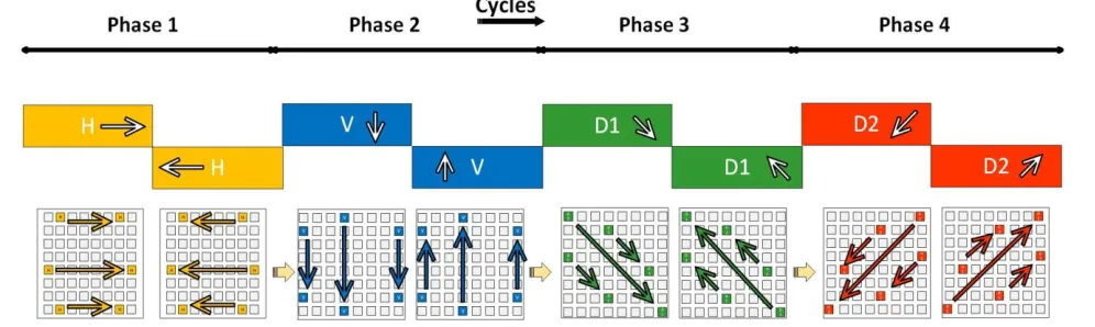
3.3. Wireless Communication Protocol
Several wireless channel access mechanisms tailored for wireless interconnections in NoC
environments are known [9] [33]. In mm-wave interconnects wireless bandwidth is limited by the
state-of-the-art transceiver design and on-chip antenna technology. To improve performance,
multiple wireless transceivers need to access the wireless medium to communicate via the
energy-efficient high bandwidth wireless interconnects. Consequently, for the proposed toroidal folding
based approach we adopt a channel access mechanism that is suitable for the 4 modes of
communication in this multichip system.
As discussed in the topology section and on the toroidal folding approach of the NoC, switches
have been deployed with the directional graphene antennas in such a way that they enable four
directions of wireless communication namely Horizontal (H), Vertical (V), Diagonal1 (D1) and
Diagonal2 (D2). As all the graphene antennas are operating in the same frequency band and the
transceiver that would be operating in different modes are very closely located in the adjacent tiles
(closer than the minimum distance for acceptably low interference), only a single mode is enabled
[image:36.612.60.558.538.687.2]
25
at a time to avoid interference amongst transceiver operating in different modes that are near to
each other. So, communication happens in four phases which are H, V, D1 and D2 as shown in Fig.
4. Each phase is further divided into 2 sub-phases that would enable half-duplex communication
between any pair using the same physical wireless channel. This is denoted by opposing arrows in
Fig. 4. The duration of each phase also plays an important role in overall performance of the whole
system. So, the duration of the phase has also been optimized to have the best performance. The
results of the optimization of phase duration has been presented in results section 4.3. Wake signals
that are being created by a simple state machine are used to enable the transceiver in their respective
phase. Therefore, a combination of separation in both space (Space Division Multiple Access) and
time (Time Division Multiple Access) enables the multi-modal communication in the proposed
graphene enabled multichip system.
3.4. Flow Control and Routing
The routing protocol for the proposed wireless NoC as well as multichip system is a seamless
intra and inter-chip data communication mechanism. Wormhole switching has been adopted for
both wired as well as the wireless links in the multichip system where data packets are broken
down into flow control units or flits [9]. Main advantage of using this kind of switching is that it
reduces the buffer requirements at the switches as unlike packet switching the whole packet is not
forwarded thereby making the switches consume less power with lower area overheads. All these
switches have their own unique addresses and bidirectional ports for all the links that are attached
to them. As the directional wireless links are point to point, even if partial packets are being
26
To optimize the network performance, we adopt a shortest path routing. A forwarding table
based routing over pre-computed Dijkstra algorithm is used. The shortest path between any two
pair of nodes is obtained by Dijkstra’s algorithm. The path between any two nodes depends on the
start node for the algorithm. However, for a specific start node the shortest path along the extracted
tree is always unique as the minimum spanning tree inherently eliminates loops. Consequently,
deadlock is avoided by transferring flits along the shortest path routing tree extracted by Dijkstra’s
algorithm, as it is inherently free of cyclic dependencies. Only header flit is forwarded to the next
switch in the path to final destination. Rest of the body flits simply follow the path that is laid by
the header flit based on the wormhole switching. So, each switch has local forwarding information
27
Chapter 4 Simulation Results and Analysis
This section gives an overview of the experimental setup of the proposed system, and evaluates
its performance in detail. The wireless architecture is a hybrid network with both wired and
wireless interconnects. The system is considered to have 64 cores per chip, and the number of
chips in the system is varied from one to a maximum of nine for this work’s experiments, yielding
different systems of sizes 64, 256 and 576 cores. Every core in the multichip system is integrated
with a NoC switch, and the switches within each independent chip are interconnected using an
intra-chip NoC architecture as explained in Chapter 3. First, we discuss the optimization of the
phase duration using this simulation platform and packet energy estimation for graphene based
inter-chip wireless links followed by the performance evaluation in the next subsections.
4.1. Simulator Setup
In this section, we evaluate the performance and energy efficiency of the proposed wireless
multichip system using a cycle accurate simulator. We compare the proposed wireless interconnect
based WiNoC & multichip system with their wireline counterparts using both synthetic and
application-specific traffic patterns.
The channel capacity of THz bands is shown to be more than 4Tbps for distances of 0.1mm
[43]. However, THz transceivers such as [42] are able to exploit around 100Gbps data rates. Also,
the maximum data rate on the wireless links is conservatively assumed to be 1/10th of the carrier
frequency [36]. Using this assumption, it is possible to achieve a data rate up to 100Gbps for a
distance of 10cm at 1 THz frequency. Hence, a wireless bandwidth of 100Gbps is used for this
work. The power consumption of the wireless links is estimated from a link budget analysis as
28
65nm standard cell libraries from Chip MultiProjects (http://cmp.imag.fr), using Synopsys. On the
other hand, the delay and energy dissipation on the intra-chip wireline links is obtained through
Cadence simulations considering the specific lengths of each link based on the established mesh
topology in the individual chips considering 20mmx20mm dies. In the Mesh based intra-chip
NoCs all wired links are considered to be single-cycle links. The delay and power dissipation
including both dynamic and static power consumption of all these components of the multichip
interconnection fabric are then incorporated in a cycle accurate simulator to evaluate the
performance and energy efficiency of different multichip systems.
The simulator characterizes the multichip architecture and models the progress of the flits over
the switches and links per cycle accounting for those flits that reach the destination as well as those
that are stalled. Ten thousand iterations were performed eliminating transients in the first thousand
iterations for the synthetic traffic patterns. For application-specific traffic, each kernel is run to
completion. In our experiments, we consider each core to be connected to a three-stage pipeline
network switch adopted from [37]. The switches are connected with other switches according to
the proposed architecture. We consider each input and output port of a switch to have 8 VCs with
a buffer depth of 4 flits for all the architectures considered in this paper. We consider a
representative maximum packet size of 16 flits with a flit size of 32 bits in our experiments unless
otherwise mentioned. While higher flit sizes are possible, it has been discussed in [38] that wide
flits increase the performance of interconnection networks marginally while requiring high area
and power overheads. All the digital components are driven by a 2.5GHz clock and 1V power
29
4.2. Energy Per bit estimation for Graphene based Intra & Inter-Chip
Wireless Links
In this subsection, we estimate the energy consumption of the graphene based inter-chip
wireless links used in our proposed multichip architecture. We develop our estimate of the energy
consumption per bit over the THz channel using the graphene based transmitters and receivers
based on the path loss model developed in [20]. To reduce the transmitted energy, we consider
using directional array of graphene antennas as proposed in [19]. Path loss in Terahertz band for
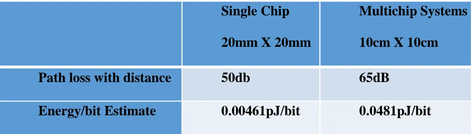
different distances are shown in [20], where, for a distance of 20mm & 10 cm at 1 THz, the path
loss is shown to be around 50dB & 65dB respectively as shown in Table 1. An antenna withunity
gain is used to estimate the path loss in [20]. Assuming free-space path loss model to be applicable
between the openings created by the quilt packaging as described in section 3.2, the effective path
loss, 𝑃𝐿𝑔 with the directional antenna array used in this work is
𝑃𝐿𝑔 = 𝑃𝐿𝑜– 𝐺𝑡𝑥– 𝐺𝑟𝑥 (1)
Where 𝑃𝐿𝑜is the sum of path loss of unity gain, and 𝐺𝑡𝑥, 𝐺𝑟𝑥 are the directional gains of transmitter
and receiver respectively. The path loss obtained from the above model is used to calculate the
power required at the transmitter. A Signal-to-Noise ratio (SNR) of 20dB is assumed for our
calculations as it provides a BER of less than 10-9 with non-coherent OOK modulation adopted in
the graphene based transmitters. The required received power for a given SNR can be computed
by
𝑃𝑟 = 𝑁𝑇
𝐸𝑅10 (𝑆𝑁𝑅10)
(2)
Where, Pr is the minimum power received by the receiver to maintain an SNR of 20dB, ER is the
antenna efficiency of the receiver, and 𝑁𝑇 is the noise power. ER refers to the ratio of the received
30
property of the graphene structure [19].The noise power considered, is primarily due to the thermal
noise in the channel and can be calculated by
𝑁𝑇 = 𝐾𝑇𝐵 (3)
Where, k is the Boltzmann constant, T is the absolute temperature and B is the bandwidth. The
transmitted power, Pt can be calculated as
𝑃𝑡 = 𝑃𝑟 𝑃𝐿𝑔 (4)
The energy required to transmit a bit from a transmitter to receiver through any wireless link is
defined as Energy per bit, 𝐸𝑏𝑖𝑡 and is given by:
𝐸𝑏𝑖𝑡 = 𝑃𝑡𝑡𝐸𝑇 (5)
Where, t is the bit duration, which is inverse of data rate and ET is the antenna efficiency of the
transmitter, which is the ratio of the radiated wireless power to the electronic power. Using (1)
-(5), the 𝐸𝑏𝑖𝑡 for a graphene based wireless link is found to be 0.0481pJ/bit considering the antenna
efficiency of 89.14% [19] and a physical bandwidth or data rate of 100 Gbps. This energy
consumption per bit is incorporated in the simulator to estimate the average packet energy of the
wireless multichip architecture proposed in this paper.
Single Chip
20mm X 20mm
Multichip Systems
10cm X 10cm
Path loss with distance
50db
65dB
[image:42.612.73.555.516.653.2]Energy/bit Estimate
0.00461pJ/bit
0.0481pJ/bit
31
4.3. Optimization of Phase Duration
In our proposed architectures, only a single mode is enabled for communication at a time to
avoid interference among transceivers in different modes as explained in section 3.3. In this
section, we optimize the duration of the phase (total duration of communication in both directions
between any pair) to provide the best performance in the NoC. We use system level simulation to
analyze the performance of the proposed systems in terms of the peak achievable bandwidth per
core at network saturation using uniform random traffic as a function of phase duration for a
proposed system of varying sizes. The peak achievable bandwidth per core is measured as the
maximum sustainable data rate in number of bits successfully routed per core per second at
network saturation. Longer phase durations will provide longer access of the wireless channel to
each wireless interface (WI) equipped with the graphene antennas potentially improving
performance. However, increasing the phase duration will eventually increase the interval between
[image:43.612.82.477.450.679.2]two consecutive channel accesses by a particular WI in a specific mode.
Fig. 5. Peak achievable bandwidth per core as a function of phase duration 20 22 24 26 28 30 32 34
5 10 15 20 25
P eak ac h eivab le ban d w id th p er cor e (G b p s)
Duration per phase (Cycles)
32
This will result in degradation in performance. This is evident from Fig. 5, where the peak
achievable bandwidth per core with different phase duration for a 1, 4 and 9 chip systems are
shown. It can be seen the peak achievable performance of the proposed wireless architecture is
maximum for the phase duration of 20 cycles. For this reason, we use phase duration of 20 for our
later simulations.
4.4. Performance Evaluation with Synthetic Traffic
There are three metrics being considered for performance evaluation of the multichip system:
Peak achievable bandwidth per core, packet energy dissipation and average packet latency. The
peak achievable bandwidth per core is given as the peak sustainable data rate in number of bits
successfully routed per core per second at network saturation. This is given as B,
B = tβf
Where, t is the maximum throughput in number of flits received per core per clock cycle at network
saturation, β is the number of bits in a flit, and f is the clock frequency. The throughput is directly
obtained from system level simulations performed by the cycle accurate simulator. The average
packet energy dissipation is defined as the average energy dissipated in transmission of a packet
from source to destination. It is given by adding the energy dissipation of all the components in
the multichip system (buffers, switches, links, etc.) and dividing this sum by the total number of
packets that were successfully routed. This total sum will always include the energy dissipation of
the WIs as they are always active in the wireless multichip system. However, for the wireline
multichip system, the energy dissipated is added to the sum only when a flit traverses.
In the following subsections, the performance of the proposed wireless single and multichip
33
compared with that of the wireline and Interposer based multichip system. This comparison
involves different interconnect architectures in total due to the consideration of single chip system
as well as different topologies for each multichip system.
i) Mesh: The first selected wireline architecture is Mesh based architecture, where each
switch, expect those are in the edges, are connected with other switches in its cardinal
directions (NSEW) using wireline interconnection to form a tile based regul