2
nd-revision
New High-Order Filter Structures Using Only
Single-Ended-Input OTAs and Grounded Capacitors
Chun-Ming Chang, Bashir M. Al-Hashimi, Yichuang Sun*, and J. Neil Ross
School of Electronics and Computer Science, University of Southampton,
Highfield, Southampton SO17 1BJ, UK E-Mail:[email protected]
*Department of Electronic, Communication and Electrical Engineering University of Hertfordshire
Hatfield Herts AL10 9AB, UK
Abstract
Despite the wealth of literature on OTA-C filters, the synthesis of high-order filter characteristics is still an active topic. In this paper the realization of voltage transfer functions based on canonical current-mode follow-the-leader-feedback (FLF) OTA-C structures are investigated. Two new structures are presented, which use only single-ended-input OTAs and grounded capacitors. The first structure has a single voltage input and multiple voltage outputs taken from different nodes, which enables it to provide simultaneous outputs of different filter functions. The second structure has a single voltage output and single voltage input distributed to different circuit nodes for a universal realization. The authors not only propose such filter structures, but also show how analytical synthesis can be used to produce filter circuits that have less active elements than those recently reported voltage-mode structures which are based on differential-input OTAs. This represents another attractive feature from chip area, and power consumption point of view. Simulation results verifying the theoretical analysis of the proposed filter structure are included.
I. Introduction
of [9-12] have one input and one output which mean that there is a different filter topology for different filtering function. In some applications, however, simultaneous outputs of different high-order filtering functions may be needed.
The aim of this paper is to present two new high-order OTA-C filter structures employing only single-ended-input OTAs, and grounded capacitors, based on the canonical current-mode FLF OTA-C filter structure [11, 12], but for the realization of voltage transfer functions. The first one is capable of providing different filtering functions (LP, HP, BP) from different nodes without changing the filter topology. This is achieved without increasing the number of active elements; in fact, it has the least number of active and passive elements when compared with some recently reported voltage-mode works including [9, 10]. The second one is obtained by adding a linear input distribution OTA network to the first one. Any voltage nth-order transfer functions can be realized by the second one which simultaneously enjoys three main attractive criteria: the minimum components, only single-ended-input OTAs, and only grounded capacitors [8].
II.
New OTA-C Filter Structure for Realizing Nth-Order Low-Pass,
Band-Pass, and High-Pass Filters of Voltage Transfer Function
Fig.1 shows the proposed nth-order filter structure where Vin is the filter input voltage, and Vout(0), Vout(1), Vout(2), Vout(3), …… , Vout(n-1), and Vout(n) are the n+1 filter voltage outputs. The settings of the n+1 filter output voltages determine the filter functions (LP, HP, BP). It can be seen that the structure employs only single-ended-input OTAs and grounded capacitors, an advantage of the current-mode FLF structure [11, 12], which is here taken for realization of voltage transfer functions.
Vout(0) +
+ +
+
+
+
-Vout(n-1)
Vout(n-2)
-Vout(1)
Vin
+ +
-Vout(n) + +
-1 1
1 1
1 1
1
1 n
n a
a
−
2 n
1 -n a
a
−
0 1 a a
, ∆ i s i a in V i out V ÷÷ ÷ ø ö çç ç è æ = ÷ø ö çè
æ for i=0, 1, 2 …, n-1, n,
where ∆= ansn +an−1sn−1+an−2sn−2+an−3sn−3+...+a1s+a0. (1) Cross multiplying the transfer function of Eq. (1) as i = 0, and re-arranging the result, we obtain å− = − − = ÷÷ ø ö ç ç è æ ÷ ÷ ø ö ç ç è
æ n 1
1
i a0
i s i a out(0) V out(0) V in V 0 a n s n a out(0)
V (2)
From Eq. (1), we have
÷÷ø ö ççè æ = − − 1 i i 1) out(i out(i) a s a V
V (i = 1, 2, 3…, n) (3)
( )
( )
( )
÷ ÷ ø ö ç ç è æ ÷ ÷ ø ö ç ç è æ − − = = 1 i a s i a 1 i out V 0 a i s i a 0 out V i outV (i = 1, 2, 3…, n) (4)
Substituting Eq. (4) into Eq. (2) gives
( )
å( )
= − − = − ÷÷ ø ö ç ç è æ n 1
i ai 1
s i a 1 i out V 0 out V in
V (5)
Eq. (5) is a voltage relationship. In order to be consistent with the input-and-output current relationship of an OTA, i.e.,
(
V+ −V−)
gm =Iout, we multiply each side of Eq. (5) by an equal transconductance of unity value (1), leading to( )
(
)
( )
( )
( )
n( ) ( )
11 i 1 1 i a s i a 1) out(i V n 1
i ai 1
s i a 1 i out V 0 out V in
V 1 1 å
ú ú û ù ê ê ë é ÷ ÷ ø ö ç ç è æ ÷ ÷ ø ö ç ç è æ = − − = å = − − =
− (6)
Then, Eq. (3) can be derived as
( )
úû ù ê ë é ÷÷ø ö ççè æ = −
− a 1
s a V V 1 i i 1) out(i
out(i) ( i = 1, 2, 3, ……, n),
namely,
( )
÷÷ø ö ççè æ = − − 1 i i 1) out(i out(i) a s a V 1
V ( i= 1, 2, 3, ……, n). (7)
(
( )
)
( )
1 n Vout( )
i( )
1 1 i 0 out V in V å = =− (8)
By using the active element, OTA, whose characteristic relationship is Iout =gmVin, and the grounded capacitor, whose admittance is sC, to implement Eq. (7), a fundamental OTA-grounded capacitor structure is obtained by a OTA-grounded capacitor (with capacitance
1 i i a a − ) connected with the output terminal of a single-ended-input OTA (with transconductance unity) having an input voltage Vout( )i and an output voltage Vout( )i−1 across the grounded capacitor. Next, we implement Eq. (8) using the output currents of the OTAs and Kirchhoff’s current law. The combination of the individual circuit yields the circuit shown in Fig. 1, in which all the coefficient values are normalized.
In summary, the proposed synthesis method has decomposed the nth-order transfer function (Eq. (1)) into n+1 transfer functions including n, 1st-order transfer functions (Eq.(7)) and one constraint equation (Eq. (8)). To illustrate the synthesis method, consider the structure generation of a 4th-order filter. The synthesis method uses Eqs. (7) and (8). Based on these equations, when n=4, the 4th-order OTA-C filter has the following three transfer functions
÷ ÷ ø ö ç ç è æ = ∆ 0 a in V out(0) V (Low-pass); ÷÷ ÷ ø ö çç ç è æ = ∆ 2 s 2 a in V out(2) V (Band-pass); ÷÷ ÷ ø ö çç ç è æ = ∆ 4 s 4 a in V out(4) V (High-pass);
where 2 1 0
2 3 3 4
4s a s a s a s a
a
∆= + + + + (9) It should be noted that, in general, a voltage follower may be necessary at the output of the
filter to buffer the output and avoid the effects of load capacitance or resistance changing the response of the filter.
III.
New OTA-C Filter Structure for Realizing Nth-Order Universal Voltage
Transfer Functions
In the above section, we proposed a new filter structure, shown in Fig. 1, for realizing nth-order OTA-C low-pass, band-pass, and high-pass filters. Eq. (1), corresponding to Fig. 1, shows that there are n+1 different-order transfer functions which can be realized at n+1 different nodes in Fig. 1, respectively. The general nth-order voltage transfer function, shown as below, 0 1 2 2 2 n 2 n 1 n 1 n n n 0 1 2 2 2 n 2 n 1 n 1 n n n in out a s a s a ... s a s a s a b s b s b ... s b s b s b V V + + + + + + + + + + + + = − − − − − − −
− (10)
is the linear combination of the n+1 different-order transfer functions shown in Eq. (1), i.e.,
å
= − − − − − − − − ú ú û ù ê ê ë é ÷÷ø ö ççè æ ÷÷ø ö ççè æ = + + + + + + + + + + + + = n 0 i i i i i 0 1 2 2 2 n 2 n 1 n 1 n n n 0 1 2 2 2 n 2 n 1 n 1 n n n in out ∆ s a a b a s a s a ... s a s a s a b s b s b ... s b s b s b V VVin +
+ +
+
+
+
+ +
-Vout
-+ +
-1
1 1
1 1
-+
+ + +
+
+
-- - -
-+ + + + + +
+ +
+ +
+
+ gb0 gb1 gb2 gb(n-3) gb(n-2) gb(n-1)
gbn ga0
ga1 ga2
ga(n-2) ga(n-1)
gan
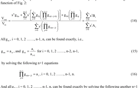
Fig.2. OTA-C filter structure II for realizing general nth-order transfer functions
Two synthesis approaches to realize the above relationship are proposed as follows.
(i) Using the linear combination method to perform the synthesis, multiply both sides of Eq. (11) by V and obtain in
( )
å
= úúû
ù ê
ê ë é
÷÷ø ö ççè
æ ÷÷ø ö ççè æ
×
= n
0
i in
i i i i
out V
∆
s a a b 1
V (12)
Then, we take each nodal voltage in the circuit structure of Fig. 1, i.e., Vout( )i (= in i
i V
∆
s a
) in which i = 0, 1, 2 ……, n-1, and n, as the input voltage of an extra OTA with the transconductancebi ai. Join all of the output terminals of the n+1 extra OTAs and connect the summing point with an equivalent grounded resistor realized by a single-ended-input OTA with unity transconductance. The realized circuit structure uses 2n+4 single-ended-input OTAs and n grounded capacitors.
(ii) A more effective synthesis approach is explained as follows. Multiply both sides of Eq. (11) by V and obtain the following other form (different from Eq. (12)) in
å
= úúû
ù ê
ê ë é
÷÷ø ö ççè æ ÷÷ø ö ççè
æ
= n 0 i
i i i i in out
∆
s a a b V
The physical meaning of the above relationship is “to insert different weights of the input voltage signal,V , into each node in the filter structure shown in Fig. 1 and then obtain the in output voltage signal”. According to this approach [1, 9, 12], giving a forward signal, with a weight of input voltage signal, from input voltage node to each inner node in the filter structure shown in Fig. 1, we obtain the other new OTA-C filter structure, shown in Fig. 2, for realizing the general nth-order voltage transfer function shown in Eq. (10). The realized circuit structure uses 2n+2 single-ended-input OTAs and n grounded capacitors.
The circuit structure (Fig. 2) of approach (ii) uses two fewer single-ended-input OTAs than that (Fig. 3) of approach (i) and is recommended to realize the general nth-order voltage transfer function shown in Eq. (10). Note that, in Fig. 2, all 2n+2 OTAs have single-ended input and all n capacitors are grounded. The numbers of active OTAs and grounded capacitors are the minimum numbers [9] to realize such a general nth-order voltage transfer function shown in Eq. (10).
In Fig. 1, although we let all the tranconductances of the OTAs be unity and let the capacitances of n grounded capacitors bea1 a0 , a2 a1, a3 a2 ……, an−1 an−2 , and
1 n
n a
[image:6.595.69.529.411.704.2]a − , in fact, all the values of the transconductances and the capacitances can be given flexibly. The restriction of the values of the transconductances and the capacitances shown in Fig. 1 is used for being consistent with the derivation process and the original given transfer functions shown in Eq. (1). Similarly, in order to simplify and clarify the network analysis of Fig. 2, we let the value of each grounded capacitor be unity although, as a matter of fact, it can be given by any different required value. Circuit analysis yields the following transfer function of Fig. 2:
å
å
å
∏
∏
å
∏
å
= =
= −
= −
−
= =
− −
= −+
−
=
=
÷÷ø ö ççè
æ ÷÷ø
ö ççè
æ
+
ú û ù ê
ë é
÷÷ø ö ççè
æ
+
= n
0
i i
i n
0
i i
i
n
0 i
i n
0 j
j) a(n i
1 n
0 j
aj b0
i
0 j
i 1 n
0 k
k) j a(i bj
1 n
1 i
i bn
n
in out
A s
B s g
s
g g
g g
s g
s V V
(14)
Allg , i = 0, 1, 2 ……, n-1, n, can be found exactly, i.e., ai
n
an a
g = , and
1 i
i
ai a
a g
+
= for i = 0, 1, 2 ……, n-2, n-1, (15)
by solving the following n+1 equations
n i i 0
j
j)
a(n a
g =
∏
=− − , i = 0, 1, 2 ……, n-1, n. (16)And allg , i = 0, 1, 2 ……, n-1, n, can be found exactly by solving the following another n+1 bi equations
[image:6.595.74.389.443.517.2]
0 1
n
0 j
aj b0
i i
1 n
0 k
k) j a(i i
0
j bj
n bn
b g g
b g
g b g
= ÷÷ø ö ççè
æ
= ÷÷ø ö ççè
æ =
∏
∏
å
−
= − −
= −+
=
, i = 1, 2 ……, n-1. (17)
In any cases, if the calculated gbj= 0, then the corresponding OTA should be eliminated; and if the calculated gbj= a negative value, then the two input terminals of the corresponding OTA should be interchanged.
The relative sensitivities, ÷
ø ö ç è æ
∂ ∂
÷ ø ö ç è æ
=
x Y Y
x SY
x , are the values of filter characteristic parameters with respect to circuit elements. If we let the values of all capacitors from the right side in Fig. 2 be C0,C1,C2...,Cn−2, and Cn−1, respectively, as we divide both numerator and denominator of its transfer function by (C0C1C2...Cn−2Cn−1), the transfer function of Fig. 2 is similar to Eq. (14) by replacing g with ai gai Ci for i = 0, 1, 2……, n-2 and n-1. Due to space limitation, only key sensitivity results are quoted without derivation. For example, the denominator coefficient sensitivities to g where i = 0, 1, 2 ……, n-1, n, are 1 or 0. The ai numerator coefficient sensitivities to g are bi
0 S n
bi B
g = for i = 0, 1, 2 ……, n-1, S bnn 1 B
g = ,
0 S 0
bi B
g = for i = 1, 2 ……, n-1, n, S b00 1 B
g = , ( )
( )
å
∏
∏
=
− −
= −+
− −
= −+
ú û ù ê
ë é
÷÷ø ö ççè
æ
÷÷ø ö ççè
æ
= i
0 j
i 1 n
0 k
k j i a bj
i 1 n
0 k
k j i a bj
B g
g g
g g
S i
bj for i= 1, 2, 3……, n-1 and j = 0, 1, 2……, i. (18)
Detailed numerator and denominator coefficient sensitivities with respect tog , ai g , and bi i
C are in the range from -1 to 1 provided that all g and ai g are positive. bi
[image:7.595.76.497.414.527.2]IV. Comparison with Previous Works and Simulation Results
Table 1 Comparison of recently reported nth-order OTA-based filters
Types of OTAs Number of
OTAs
Nth-order general filter in [9]
Nth-order general filter in [10]
Nth-order proposed filter
(Fig. 2)
2n+2
3n+3 2n+2
Single-input (n+2),
Double-input (n) Single-input (3n+2),
Double-input (1) Single-input
(2n+2) Parameters
Cases
Nth-order proposed filter
(Fig. 1)
n+2 Single-input
(n+2)
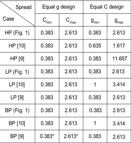
[image:8.595.166.433.459.750.2]Another parameter which needs to be compared with one another is the span (or spread) of filter component values which may be large for high-order filters. A wider span of filter component values leads to a worse implementation carried out in CMOS which will create the quadratic current ratios. To give insight into what the component spread of the new filter structure shown in Fig.1, Table 2 provides the comparison of the fourth-order Butterworth high-pass (HP), low-pass (LP), and band-pass (BP) filters designed using the proposed filter (Fig.1) and those reported in [9, 10]. The Table gives the component spread for equal transconductance (g) and equal capacitance (C) designs. It can be seen that the proposed filter has the same component spread (equal g design) as those in [9, 10] except the case for band-pass in [9]. In the case of equal C design, the filter in [10] has the least component spread, and our filter has better component spread than that in [9].
Table 2 Component spread comparison of the fourth-order HP, LP, and BP Butterworth filters
Spread Equal g design Equal C design
Cmin Cmax gmin gmax Case
HP (Fig. 1)
HP [10]
HP [9]
LP (Fig. 1)
LP [10]
LP [9]
BP (Fig. 1)
BP [10]
BP [9]
0.383
0.383
0.383
0.383
0.383
0.383
0.383
0.383
0.383*
2.613
2.613
2.613
2.613
2.613
2.613
2.613
2.613
2.613*
0.383
0.383
0.383
0.383
0.383
0.383
2.613
2.613
2.613
2.613
2.613 1
1
3.414
3.414 11.657 0.635 1.617
To verify the theoretical analysis of the proposed filter structure shown in Fig.1, a third-order low-pass and high-pass OTA-C filter has been simulated using H-Spice with the UMC05 level-49 parameters, with W/L=5µ/1µ for NMOS and 10µ/1µ for PMOS transistors, and the component values: (i) g0,1,2,3,4=56µS (Ib=8.852µA), C1=18pF, C2=9pF, and C3=4.5pF for the responses with fo=0.990MHz, using Vdd=2.5V, and Vss=-2.5V, (ii) g0,1,2,3,4=62.8µS (Ib=10.495µA), C1=10pF, C2=5pF, and C3=2.5pF for the responses with fo=1.999MHz, using Vdd=2.5V, and Vss=-2.5V. The OTAs were implemented using the CMOS circuit given in [13]. Fig. 3 shows the simulated low-pass and high-pass responses of the filter. As can be seen there is a close agreement between theory and simulation, for example, the simulated 3dB frequencies are 0.94MHz (high-pass) and 1.04MHz (low-pass), compared to 0.990MHz in the ideal case, and 1.83MHz (high-pass) and 2.02MHz (low-pass), compared to 1.999MHz in the ideal case. Other filters with different order and responses were also simulated and found to perform as theory predictions.
V. CONCLUSION
This paper has presented two new high-order filter structures (shown in Figs. 1 and 2) that employ only single-ended-input OTAs and grounded capacitors. It has been shown how decomposing analytically an nth-order transfer function into n+1 simple realisable transfer functions using OTA-C circuits produces the first filter structure that employs less active elements than some of the recently reported methods and offers simultaneous multiple outputs. The proposed first filter structure has n+2 single-ended-input OTA, and n grounded capacitors for a given filter order, n. Realizing the general transfer function by using the more effective synthesis approach different from the linear combination of each output signal of the first filter structure leads to the second filter structure which can realize any kind of voltage transfer functions employing the minimum components, only 2n+2 “single-ended-input” OTAs, and only n “grounded” capacitors.
ACKNOWLEDGEMENTS
The authors would like to thank the anonymous reviewers for their constructive comments.
REFERENCES
[1] T. Deliyannis, Y. Sun, and J. K. Fidler, Continuous-time active filter design, CRC press, Florida, USA, 1999.
[2] M. A. Tan, and R. Schaumann, “Simulating general-parameter LC-ladder filters for monolithic realizations with only transconductance elements and grounded capacitors”, IEEE Trans. Circuits Syst., vol. 36, no. 2, pp. 299-307, Feb. 1989.
[3] P. V. Ananda Mohan, “Novel OTA-C filter structures using grounded capacitors”, Proc. IEEE ISCAS, pp. 1347-1350, 1991.
[4] Y. Sun, and J. K. Fidler, “OTA-C realisation of general high-order transfer functions”, Electron. Lett., vol. 29, no. 12, pp. 1057-1058, June 1993.
[6] R. Schaumann, “Simulating lossless ladders with transconductance circuits”, IEEE Trans. Circuits Syst.-II, vol. 45, pp. 407-410, March 1998.
[7] Y. Sun, “OTA-C filter design using inductor substitution and Bruton transformation methods”, Electron. Lett., vol. 34, no. 22, pp. 2082-2083, Oct. 1998.
[8] Y. Sun, and J. K. Fidler, “Synthesis and performance analysis of universal minimum component integrator-based IFLF OTA-grounded capacitor filter”, IEE Proc.-Circuits Devices Syst., vol. 143, no. 2, pp. 107-114, Apr. 1996.
[9] Y. Sun, and J. K. Fidler, “Structure generation and design of multiple loop feedback OTA-grounded capacitor filters”, IEEE Trans. Circuits Syst.-I, vol. 44, no. 1, pp. 1-11, Jan. 1997.
[10] C. A. Barbargires, “Explicit design of general high-order FLF OTA-C filters”, Electron. Lett., vol. 35, no. 16, pp. 1289-1290, Aug. 1999.
[11] Y. Sun and J. K. Fidler, “Current-mode multiple-loop feedback filters using dual-output OTAs and grounded capacitors”, Int. J. of Circuit Theory and Applications, Vol. 25, pp. 69-80, 1997.
[12] Y. Sun and J. K. Fidler, “Current-mode OTA-C realisation of arbitrary filter characteristics”, Electron. Lett., Vol. 32, No. 13, pp. 1181-1182, June 1996.
[13] S. Szczepanski, A. Wyszynski, and R. Schaumann, “Highly linear voltage-controlled CMOS transconductors,” IEEE Trans. Circuits Syst.-I, vol. 40, no. 4, pp. 258-262, Apr. 1993.
105 106 107
-80 -70 -60 -50 -40 -30 -20 -10 0
frequency(Hz)
m
ag
ni
tud
e(
db)
-:theoretical o,triangle:simulation
![Table 1 shows a comparison in terms of number of OTAs and types of OTAs between the proposed filter structures (Figs.1 and 2), and those recently reported in [9] and [10]](https://thumb-us.123doks.com/thumbv2/123dok_us/8516415.351723/7.595.76.497.414.527/table-comparison-number-proposed-filter-structures-recently-reported.webp)