City, University of London Institutional Repository
Citation
:
Zhang, H., Zhou, L., Lu, L., Chen, J. and Rahman, B. M. ORCID:
0000-0001-6384-0961 (2018). Non-volatile Optical Switch Based on a GST-Loaded Directional Coupler.
Paper presented at the 2018 the 3rd Optoelectronics Global Conference (OGC 2018), 4-7
Sep 2018, Shenzhen, China.
This is the accepted version of the paper.
This version of the publication may differ from the final published
version.
Permanent repository link:
http://openaccess.city.ac.uk/id/eprint/21127/
Link to published version
:
http://dx.doi.org/10.1109/ogc.2018.8529888
Copyright and reuse:
City Research Online aims to make research
outputs of City, University of London available to a wider audience.
Copyright and Moral Rights remain with the author(s) and/or copyright
holders. URLs from City Research Online may be freely distributed and
linked to.
City Research Online:
http://openaccess.city.ac.uk/
[email protected]
Non-volatile optical switch based on a GST-loaded directional coupler
Hanyu Zhang, Linjie Zhou, Liangjun Lu, and
Jianping Chen
Shanghai Institute for Advanced Communication and Data Science, Shanghai Key Lab of Navigation and Location Services, State Key Laboratory of Advanced
Optical Communication Systems and Networks Department of Electronic Engineering, SJTU
Shanghai, China
B. M. A. Rahman
Department of Electrical and Electronic Engineering City, University of London
London, U.K.
Abstract—We present a non-volatile optical switch based on a directional coupler comprising a silicon-Ge2Sb2Te5(GST) hybrid waveguide. The non-volatility of GST makes it attractive for reducing static power consumption in optical switching. Experimental results show that the optical switch has an extinction ratio of >20 dB in the bar state and >25 dB in the cross state around 1578 nm wavelength. The insertion loss is 2 dB and 7 dB for the bar and cross states, respectively.
Keywords-silicon photonics; phase change material; directional coupler
I. INTRODUCTION
A directional coupler (DC) is a basic component in integrated photonics that couples light propagating in a waveguide to another parallel waveguide placed in close proximity. The operation principle of the DC can be explained by the coupled mode theory. It has been widely used in optical switches [1], multiplexers/de-multiplexers [2] and polarization beam splitters [3] etc. On the other hand, tunable silicon photonic devices are based primarily on the thermo-optic (TO) effect or the free carrier dispersion effect (FCD). They are both volatile and require constant power to maintain tuning. The power consumption can be reduced considerably, if the refractive index change can be maintained using a non-volatile tuning method.
Phase change materials (PCMs) have a striking portfolio of properties [4]. They can be rapidly and reversibly switched between amorphous (am) and crystalline (cr) states. The Ge2Sb2Te5 (GST) material, as a PCM commonly used in
optical storage, exhibits distinct optical (refractive index) and electrical (resistance) properties between its amorphous and crystalline states [5]. Besides, its phase change is reversible and does not degrade material properties after multiple phase transitions [6]. In addition, this material possesses the “self-holding” feature [7], and consequently there is no need for static power consumption to maintain the states. Hence, this feature can be utilized to manipulate light propagation and implement reconfigurable non-volatile optical devices.
In this paper, we demonstrate an optical switch based on a DC. The DC is composed of a silicon waveguide coupled with a GST-loaded silicon waveguide. The propagation constant of the GST-loaded silicon waveguide can be adjusted by changing the GST phase state. We use the
finite-difference eigenmode (FDE) solver to calculate the waveguide mode and three-dimensional finite-difference time-domain (3D-FDTD) method to calculate the optical transmission. Experimental results show that the optical switch can achieve >20 dB extinction ratio (ER) for both switching states around the operation wavelength. The cross state has a higher insertion loss (IL) of 7 dB.
II. NUMERICAL SIMULATION
Fig. 1 shows the complex refractive index (n+ik) of radio-frequency (RF) sputtered GST film in dependence of wavelength, measured by ellipsometry. Reversible switching of GST by optical or electrical pulses has been demonstrated in the literature [4]. It can be seen that due to the significant change in bonding, the refractive index of GST is increased considerably when GST is changed from an amorphous state to a crystalline state [8].
Figure 1. Real and imaginary parts of GST material refractive index changing as a function of wavelength. aGST: amorphous GST; cGST: crystalline GST.
[image:2.612.322.546.427.592.2]achieve the phase matching condition in the am-GST state. The under-cladding of the silicon waveguides is SiO2 and the
upper-cladding is air. In our simulation, the refractive indices of silicon and silica are taken as 3.4764 and 1.444, respectively.
Figure 2. Schematic structure of the optical switch. Inset shows the cross-sectional view of the coupled waveguides.
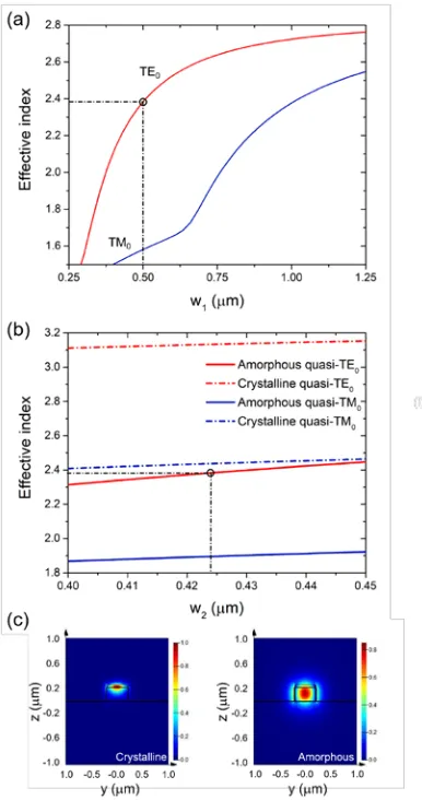
Fig. 3(a) shows the calculated effective indices of the fundamental transverse electric (TE0) and transverse
magnetic (TM0) optical modes of the silicon waveguide
changing with waveguide width w1 at 1550 nm wavelength.
We choose w1 = 500 nm, corresponding to an effective index
of 2.384 for the TE0 mode as indicated by the dotted line.
Fig. 3(b) shows the real effective index of the TE0 and TM0
optical modes of the GST-loaded silicon waveguide changing as a function of w2 when GST is in the am and cr
states. When w2 = 424 nm, the real effective index of the
GST-loaded waveguide is 2.384 for the am state, equal to that of the silicon waveguide. The Ey intensity distributions
of the waveguide modes are presented in Fig. 3(c). The optical field is mainly confined in the silicon waveguide when GST is in the am state, while it is localized more into the GST layer when it is in the cr state. This results in a large difference in their effective indices. Therefore, light can efficiently couple from the silicon waveguide to the GST-loaded silicon waveguide in the am state due to the matched propagation constant. When GST is changed to the cr state, light can no longer couple to the other waveguide. This is the basic operation principle of the phase-change enabled optical switch.
We set the gap size between the two waveguides to be g = 230 nm. Fig. 4 illustrates the Ey intensity profiles for the
two super-modes of the coupled waveguides. In the am state, the two waveguides are strongly coupled, with the super-modes exhibiting an even-mode and an odd-mode. In the cr state, however, the two waveguides are weakly coupled, with the super-modes approaching the individual waveguide modes. Table 1 summarizes the extracted refractive indices of the two super-modes.
Figure 3. (a) Effective indices of two lowest-order modes in the silicon waveguide. (b) Real effective indices of two lowest-order modes in the GST-loaded silicon wavegudie. (c) Wavegudie mode Ey intensity
distributions in the GST-loaded silicon waveguide.
Fgure 4.Electric field Ey intesity distributions in the coupled waveguides
[image:3.612.339.532.72.438.2] [image:3.612.59.296.128.318.2] [image:3.612.334.535.491.680.2]TABLE 1. EFFECTIVE INDEX OF THE SUPER-MODES IN THE COUPLED WAVEGUIDES.
GST phase Super-mode 1 Super-mode 2
Amorphous 2.3892+0.000325i 2.3795+0.00042i
Crystalline 3.1342+0.6378i 2.385+3.225e-5i
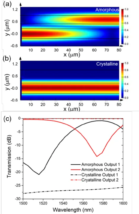
Fig. 5 (a) and (b) show the simulated light propagation in the coupled waveguide for two GST states. When the GST is amorphous, the two coupled waveguides satisfy the phase matching condition, and the input light launched into the silicon waveguide is evanescently coupled into the GST-loaded silicon waveguide. The cross-over coupling length is 80 µm. When the GST film is crystallized, the input light cannot be coupled into the GST-loaded silicon waveguide and is thus remained in the original silicon waveguide. The simulated transmission spectra are shown in Fig. 5(c). It can be seen that the optimal operation wavelength is around 1578 nm, where the extinction ratio in the am state reaches the maximum.
Figure 5. (a, b) Light propagation in the directional coupler when GST is (a) amorphous and (b) crystalline. (c) Transmission spectra of the two output ports in amorphous and crystalline states.
III. DEVICE FABRICATION
We fabricated the device on a SOI wafer. The wafer was first cleaned by acetone, isopropanol (IPA) and deionized (DI) water in sequence and then baked for 2 minutes at 180 °C temperature. Next, the wafer was spin-coated with ZEP-520 e-beam resist, and prebaked for 3 minutes at 180°C. We used e-beam lithography to define the silicon waveguide patterns. The e-beam resist was developed in IPA/MIBK (3:1). The pattern was transferred to the silicon layer with inductively-coupled plasma (ICP) dry etch. The residual e-beam resist was completely removed by N-Methyl pyrrolidone (NMP). The GST deposition window was opened using the second e-beam lithography process. A 40-nm-thick GST film was then sputtered on the wafer using an RF sputtering system from a stoichiometric Ge2Sb2Te5 target
[image:4.612.320.551.304.498.2](20 W, 15 s.c.c.m. Argon gas, 0.0889 nm/min deposition rate). Finally, the lift-off process was used to remove the GST outside the deposition window in a warm acetone bath. Fig. 6 shows the scanning electron microscope (SEM) image of the fabricated device.
Figure 6. Scanning electron microscope image of the fabricated device. The inset shows the zoom-in of the directional coupler.
IV. EXPERIMENTAL RESULTS AND DISCUSSION
[image:4.612.58.293.313.675.2]The bar-port (output 2) insertion loss is around 2 dB with the bandwidth >100 nm. The extinction ratio between the two ports is >20 dB for the 100 nm wavelength range. When GST is amorphous, the coupling is sensitive to wavelength. This is because both the cross-over coupling and the exact phase match can only be achieved at a single wavelength. The maximum transmission of the cross-port (output 1) is achieved at the 1578 nm wavelength. The insertion loss is 7 dB and the maximum extinction ratio is >25 dB.
Figure 7. Measured transmission spectra of the device when GST is at (a) crystalline and (b) amorphous states. The insets show the extinction ratio curves.
The insertion loss in the cross state (am-GST) is mainly caused by the GST material loss (absorption loss and surface roughness induced scattering loss). In fact, The GST material can be replaced by other low-loss materials, such as GeSe [9] and Ge2Sb2Se4Te1 [1] etc. They have a lower loss at the 1550
nm wavelength, which are worth further exploration in the future work. In addition, in order to realize a broadband directional coupler, we can design an adiabatic directional
coupler. The width of one waveguide increases while the width of the other waveguide decreases. The phase match condition at different wavelengths can always be satisfied at a certain coupling point along the directional coupler. The coupler length should be longer in order to get efficient coupling.
V. CONCLUSIONS
We have demonstrated a non-volatile optical switch based on a directional coupler comprising a silicon-GST hybrid waveguide. GST is a phase change material that exhibits a large difference in refractive index between a crystalline state and an amorphous state. In addition, GST’s non-volatile nature provides a self-holding feature for the switch, allowing the switch states to be maintained without static power. The directional coupler length is 80 µm. Experimental results exhibit that the optical switch has an ER of >20 dB in the bar state in a wide spectral range and >25 dB in the cross state near the optimal coupling wavelength of 1578 nm. The IL is 2 dB for the bar state and 7 dB for the cross state. The performance can be further improved by using low-loss phase change materials.
ACKNOWLEDGMENT
This work was supported in part by the National Natural Science Foundation of China (NSFC) (61422508, 61535006, 61705129, 61661130155).
REFERENCES
[1] Q. Zhang, Y. Zhang, J. Li, R. Soref, T. Gu, and J. Hu, "Broadband nonvolatile photonic switching based on optical phase change materials: beyond the classical figure-of-merit," Opt. Lett., vol. 43, no. 1, pp. 94-97, 2018.
[2] W. Jiang, "Ultra-compact and fabrication-tolerant mode multiplexer and demultiplexer based on angled silicon waveguides," Opt. Commun., vol. 425, pp. 141-145, 2018.
[3] Y. Kim, M. H. Lee, Y. Kim, and K. H. Kim, "High-extinction-ratio directional-coupler-type polarization beam splitter with a bridged silicon wire waveguide," Opt. Lett., vol. 43, no. 14, p. 3241, 2018. [4] M. Wuttig, H. Bhaskaran, and T. Taubner, "Phase-change materials
for non-volatile photonic applications," Nat. Photon., vol. 11, no. 8, pp. 465-476, 2017.
[5] J. Feldmann et al., "Calculating with light using a chip-scale all-optical abacus," Nat. Commun., vol. 8, no. 1, p. 1256, 2017. [6] M. Stegmaier, C. Ríos, H. Bhaskaran, C. D. Wright, and W. H. P.
Pernice, "Nonvolatile all-optical 1 × 2 switch for chipscale photonic networks," Adv. Opt. Mater., vol. 5, no. 1, p. 1600346, 2017. [7] S. Raoux, F. Xiong, M. Wuttig, and E. Pop, "Phase change materials
and phase change memory," MRS Bulletin, vol. 39, no. 08, pp. 703-710, 2014.
[8] K. Shportko, S. Kremers, M. Woda, D. Lencer, J. Robertson, and M. Wuttig, "Resonant bonding in crystalline phase-change materials," Nat. Mater., vol. 7, no. 8, pp. 653-8, 2008.
[9] R. Soref, "Phase-change materials for Group-IV electro-optical switching and modulation," 12th International Conference on Group IV Photonics, pp. 157-158, Vancouver, Canada, 2015.
[image:5.612.56.289.175.546.2]![Fig. 1 shows the complex refractive index (nchange in bonding, the refractive index of GST is increased considerably when GST is changed from an amorphous state in the literature [4]](https://thumb-us.123doks.com/thumbv2/123dok_us/1395843.92677/2.612.322.546.427.592/complex-refractive-nchange-refractive-increased-considerably-amorphous-literature.webp)