This is a repository copy of
Cyclic twinning and internal defects of boron-rich nanowires
revealed by three-dimensional electron diffraction mapping
.
White Rose Research Online URL for this paper:
http://eprints.whiterose.ac.uk/76335/
Version: Published Version
Article:
Fu, Xin and Yuan, Jun orcid.org/0000-0001-5833-4570 (2013) Cyclic twinning and internal
defects of boron-rich nanowires revealed by three-dimensional electron diffraction
mapping. Nanoscale. pp. 9067-9072. ISSN 2040-3372
https://doi.org/10.1039/c3NR01839C
[email protected]
https://eprints.whiterose.ac.uk/
Reuse
Items deposited in White Rose Research Online are protected by copyright, with all rights reserved unless
indicated otherwise. They may be downloaded and/or printed for private study, or other acts as permitted by
national copyright laws. The publisher or other rights holders may allow further reproduction and re-use of
the full text version. This is indicated by the licence information on the White Rose Research Online record
for the item.
Takedown
If you consider content in White Rose Research Online to be in breach of UK law, please notify us by
analysing the three-dimensional (3D) electron diffraction intensity distribution. Not only can the cyclic twinning structure of these nanowires be easily determined, the new approach also reveals the heterogeneous strain relaxation within the intact nanowire, through the accurate determination of the orientation relationship between the constituent crystallites. The quantitative analysis of the fine structure in the 3D diffraction dataset indicates that this may be related to the distribution of defects such as stacking faults, microtwins and dislocations. It is envisaged that the non-destructive nature of this approach could open the way for the in situ study of the structural evolution of complex nanomaterials and polycrystalline materials in general.
Introduction
In recent years, both material growth energetics and kinetics have been explored to produce a wide range of nanomaterials with interesting structures and form factors, such as nano-tetrapods,1
icosahedral nanoparticles,2
decahedral nano-particles,2,3 nanowires,4–8 and nanostars,9 to just name a few well-known examples. Identication and characterization of those complex nanostructures have always been a challenge. Real-space imaging through transmission electron microscopy is the conventional tool of choice to study the internal structure of materials, but it cannot be realized routinely with atomic resolution even using state-of-the-art aberration corrected microscopic techniques because of the large dimensions of the nanostructures involved in many cases. In general, the atomic resolution electron microscopy is a destructive structural char-acterization technique for complex nanostructures,10,11
due to the need for preparing ultrathin cross-sectional samples, yet the knowledge on the structure of intact complex nanostructures maybe important as it could be the key behind the enhanced mechanical,12,13
optical9,14
and catalytic properties of the
nanostructures.1,9 Non-destructive characterization of the nanostructures can be achieved through real-space electron tomography,15however it oen suffers from a‘missing wedge’ problem,16and it cannot yet routinely be used to determine the crystallographic information about the internal structure such as orientation relationship and internal strains.
In this paper, we will demonstrate an application of 3D intensity analysis of electron diffraction to a non-destructive study of the internal structure of a cyclic twinned nanowire. Until now, analysis of electron diffraction distribution has only been applied to the determination of crystal structures and the morphology of single crystalline nanoparticles.17–20 Here we apply the 3D diffraction intensity mapping to reveal informa-tion about polycrystalline materials for which cyclic twinned nanowires are special cases with the crystalline components joined by twinning planes. The cyclic twinning nanostructure can have real or pseudove-fold symmetry that is not seen in the bulk materials, usually it is always due to the result of a balance between the surface energy minimization and the reduction of the strain energy associated with such poly-crystalline structures.21,22
The twinning structure may be a factor inuencing the mechanical properties of nanomaterials. For example, ve-fold cyclic twinned silver nanowires exhibit anomalous strength and brittle failure.12
We will show that the retrieval of 3D diffraction intensity distribution allows us to not only identify the cyclic twinned structure directly, but the technique also reveals quantitatively the orientation relation-ship of the internal crystallites and information about defor-mation and defects associated with the internal strain relaxation, all non-destructively.
The complex nanostructure we choose to study as a model system is boron-rich cyclic twinned nanowires that have shown
aGeneral Research Institute for Nonferrous Metals, Beijing 100088, PR China. E-mail:
bDepartment of Physics, University of York, York YO10 5DD, UK. E-mail: jun.yuan@
york.ac.uk
†Electronic supplementary information (ESI) available: Crystal structure of boron carbide, experimental geometry and diffraction pattern registration for the reconstruction of the reciprocal 3D volume, data process for 3D reciprocal volume visualization, rhombohedral lattice parameter renement of the boron carbideve-fold cyclic twinned nanowire under investigation in this paper, and extinction distance evaluation of (112)rreection of boron carbide. See DOI:
10.1039/c3nr01839c
Received 12th April 2013 Accepted 1st July 2013
DOI: 10.1039/c3nr01839c
www.rsc.org/nanoscale
promising applications, such as high temperature thermoelec-tric nanomaterials23 and reinforcing phases in ceramic composites.24The boron-rich materials (B
6O, B4C,etc.) share a
common a-rhombohedral crystalline structure with a space
groupR3m(no. 166).25Despite its complexity, the best way to understand the rhombohedral unit cell is to consider it as a distorted cubic close packing structure with the lattice points occupied by nominally B12 icosahedral clusters and charge
balancing atoms such as carbon or oxygen atoms occupying the interstitial sites within this lattice (see Section 1 in the ESI†). Our early studies7,8
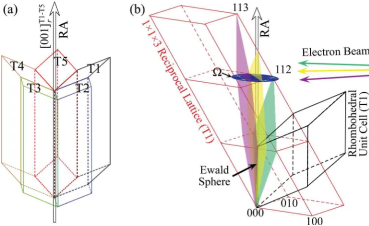
suggest that these multiply twinned nano-wires can be understood as a cyclic twinning ofve such elon-gated tetrahedral crystallites sharing a common [001]r axis
(Fig. 1a), where the subscript r refers to the rhombohedral representation.
Experimental methods
The 3D reconstruction of diffraction intensity distribution is conducted by recording the two-dimensional electron diffrac-tion patterns as a funcdiffrac-tion of systematic tilting of either the incident electron beams or the nanowires (see Section 2 in the ESI†). As the Ewald sphere (which can be approximated as a plane for the scattering of the high energy electron beam typi-cally used in the medium-voltage transmission electron microscopes) intersects with the reciprocal lattice convolved with the shape function of the truncated crystallites, the three-dimensional diffraction intensity distribution can be mapped out through systematic tilting. To study cyclic twinned nano-structures, we have chosen to examine a region of the reciprocal space where the contributions from all the twinning elements
form a symmetrical group around the nanowire axis. Fig. 1b shows a real space rhombohedral unit cell of one of the crys-talline components labelled T1 in Fig. 1a, together with a part of the corresponding reciprocal lattice structure. The (112)rand
(113)rare the two reections close to the [001]raxial direction of
the nanowire, and they are included in the 3D reconstruction of electron diffraction intensity distribution. For clarity, the other four equivalent (112)rand (113)rreections for the remaining
crystallites labelled as T2–T5 are not drawn. The scanning of the Ewald sphere through the reciprocal space is achieved through real-space tilting of the nanowire about an axis perpendicular to both the direction of the incident beam and the axis of the nanowire. The tilting is conducted with a regular angular spacing of 0.1and an overall tilting range of10. Because the
resulting tilting of the diffraction pattern is pivoted about the origin of the reciprocal space (dened to be the end of the scattering vector of the incident beam), the volume of the reciprocal space is not sampled uniformly. We have taken this into account and the experimental data shown here have all been converted into a representation with uniform voxels (see Section 3 in the ESI†).
Results and discussion
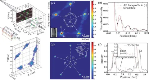
Fig. 2a shows the experimental result for one such nanowire. We can see clearly two groups ofve diffraction peaks situated about a common axis along the axial direction of the nanowire. They form two pentagonal patterns, related by inversion, which can be indexed to the grouping of the (112)rand (113)rre
ec-tions, respectively, about the axial direction of the nanowire as shown in Fig. 1b. This result directly conrms the cyclic nature
Fig. 1 (a) A structural model of afive-fold cyclic twinned boron carbide nanowire. (b) The orientation relationship between the rhombohedral unit cell in one of the
five components of the cyclic twinned nanowire (shown in black) and the corresponding reciprocal lattice (as shown in red color). Also shown are diffraction patterns, corresponding to the intersection of the reciprocal lattice points by the Ewald spheres (which are approximated by planes of different colors, corresponding to various plane waves of different incident angles). TheUplane is defined to be perpendicular to the rotation axis (RA) of the nanowires and passes through the (112)rlattice
point, so it will contain peak intensities of allfive (112)rreflections of the cyclic twinned nanowire as labelled.
Nanoscale Paper
Published on 05 July 2013. Downloaded by University of York on 28/08/2013 20:10:52.
[image:3.595.112.480.49.275.2]of twinning in the boron-rich ve-fold twinned nanowires.7,8 Compared to the more conventional methods of identifying the cyclic twinning internal structure in decahedral nanowires, which requires either one-offdestructive cross-sectional sample preparation11
or taking systematic zone-axis diffraction patterns by rotating the nanowire about its axial direction by18,4,7,8
3D diffraction intensity mapping is visually direct and requires a much smaller tilting range (about10) and can be done
non-destructively. The latter is important for in situexperimental investigation of the structural changes inside nanowires, an important area of development in nanoscience research.26
New information can be deduced by studying the three-dimensional reconstruction of the diffraction intensity in detail. We focus on theve-fold (112)rreections as shown in
Fig. 2b. A striking feature is the large difference between the intensity distributions of theve reections, showing the inhomogeneous nature of the internal structure of the nanowire. However, it is still possible to dene a point, labelled‘O’, equidistant from the peaks of allve reections in the cross-sectional map of theve (112)rreections shown
in Fig. 2c. We regard it as the projection of the [001]r axial
direction of the nanowire on the cross-sectional map. This is supported by the measurement of angles sustained by each reection with respect to the nanowire axis. They are found to be in the range of 8.1–8.5, consistent with the angle of
8.4between [001]
rand (112)rreections, calculated using the
rhombohedral lattice parameters dened for this boron carbide nanowire (see Section 4 in the ESI†). Therefore, it can be concluded that all ve twinning segments of the boron carbide nanowire share the same growth axis, i.e. the common [001]r twinning axis.
Using the axial direction of the nanowire that we have deduced, we cannd out the dihedral angles sustained by each pair of neighbouring planes formed by the (112)rreections and
the nanowire axis. They dene the orientation relationship between the neighbouring crystallites, and more signicantly they are also found to be all different, as shown in Fig. 2c. Two of the dihedral angles are about 78, while the other two are
about 66, very different from the average value of 72expected
of the uniformly strained twin boundary27,28 or the 73.68
expected of the unstrained twining structure. As we have mentioned before, intrinsic strain is known to be important for decahedral nanostructures because there is an angular mist in joiningve regular crystallites by twinning operation alone.2,21 For example, in face centered cubic (fcc) materials, there is a well-known angular deciency of 7.35 in decahedral
nano-structures and it is the cause of the intrinsic strain in the fcc cyclic twinned systems such as Au, Ag and Cu nanoparticles and nanowires or that of the related semiconductors (Si, Ge or dia-mond) and has been subject of extensive studies (see ref. 2 and 21). Using the result of cross-sectional transmission electron microscopy performed on samples prepared by a microtome
Fig. 2 (a) 3D reconstruction of the diffraction intensity distribution in the reciprocal space around (112)rand (113)rlattice points from a boron carbidefive-fold
twinned nanowire whose orientation is shown at the lower left corner. The plane defined by the peak intensities of allfive (112)rreflections is shaded and is labelled as
theUplane, as shown in Fig. 1. (b) The magnified view of the 3D distribution of the (112)rreflections is shown in (a). (c) The 2D intensity distribution of the (112)r
reflections in theUplane, with the corresponding boron carbide nanowire with a diameter of about 80 nm is shown in the inset. (d) The 2D intensity map in theUplane calculated for the idealfive-fold cyclic twinned nanowire structure whose cross-sectional view is illustrated in the inset. (e) The comparison of the experimental and simulated intensity profiles along the line AB is indicated in (c). (f) Intensity profiles across the (112)rdiffraction peaks of different crystalline segments, the inset is the
magnification of the area in the dashed rectangle.
[image:4.595.58.539.55.314.2]technique, Chenet al.11have discovered that the mis
t angle of 7.35 is shared by three crystallites in a silver cyclic twinned
nanowire with a diameter of 100 nm. However, as Ag nanowires are easily deformed, one has to be careful in extrapolating this result to the intact nanowires.
In the case of boron carbide cyclic twinned nanowires under investigation, because the dihedral angle between neighbour-ing {100}rtwinning planes is about 73.68, there is an‘angular
excess’of about 8.4when joiningve boron carbide crystallites
by {100}r-type twinning. In contrast to the silver nanorods where
three of the dihedral angles are very close to the dihedral angle between the {111}fcctwinning planes,11our result showed for
therst time, on an intact boron-rich nanowire, that none of the ve grain boundaries have the pure wedge angle expected of the single twinning relationship.
We can learn more about the possible structural features present by analyzing thene structure in the individual (112)r
reection peaks and their ares (or streaks). However to understand them quantitatively, we need to take into account thenite beam coherence, which is different in the transverse and longitudinal beam directions (Xdirection andYdirection in Fig. 2c, respectively). We estimated the transverse coherence length of the incident beam to be about 22 nm from its angular width (about 0.045 nm 1, aer being deconvoluted out of the
instrumental broadening effect) without the beam passing through the sample. The transverse coherence is about the same size as the dimension of the crystallites in the cross-sectional plane. Together with the much longer longitudinal coherence length of the beam, the individual components of these cyclic twinned nanowires will be considered to be approximately coherently illuminated in the cross-sectional plane. Examination of the angular widths of the ve (112)r
reections along the axial direction of the nanowire shows that they are in the range of 0.047–0.063 nm 1. These values are similar to the angular width for the incident beam, but signif-icantly smaller than the typical angular widths of the (112)r
reections seen in the cross-sectional map (Fig. 2c). This shows that the microstructure present in the nanowire is mostly axial. So we will focus on the features in the cross-sectional intensity map now.
The are in the diffraction patterns of a nite sized nano-structure is known to be affected by shape factors,20
strain and surface relaxation.29,30
The possible presence of theare (or the diffuse scattering) has been known because they, for example, are believed to contribute to the forbidden reections in the zone-axis diffraction patterns.31,32
The advantage of the 3D diffraction dataset is that it allows us to analyze the intensity of the diffuse scattering more quantitatively. For example, the pure shape effect can be easily simulated. Because of the long extinction distance for boron-rich materials (see Section 5 in the ESI†), a simple kinematic calculation is sufficient. This has been carried out for an ideal ve-fold cyclic twinned boron carbide nanowire (i.e. without strain and defects) with the same diameter of 80 nm as that shown in the inset of Fig. 2d and the result is shown in Fig. 2d. A comparison of the simulation and the experimental line proles along the A–B line marked in the experimental intensity map of Fig. 2c shows a good agreement both in the relative intensity and the pitch of oscillation (0.04 nm 1) (Fig. 2e). However, the simu-lation result based on an ideal shape effect cannot explain the intenseares along the directions linking (112)rreections of T3
and T4, as well as those between T2 and T3 (Fig. 2f).
We believe that these anomalousares are due to the pres-ence of stacking faults (SF) and microtwins (MT) that are common in such nanowires.23,33Fig. 3 shows the high resolu-tion transmission electron microscopy (HRTEM) evidence of their presence in the T3 and T4 crystallites of the nanowire. As a result of the stacking faults or microtwins, the widths of the defect-free regions in T3 are reduced to about 11 nm and 13 nm. This is comparable with the observed spacing of the ripples in theare from the (112)rreection of T3 to that of T4 (about
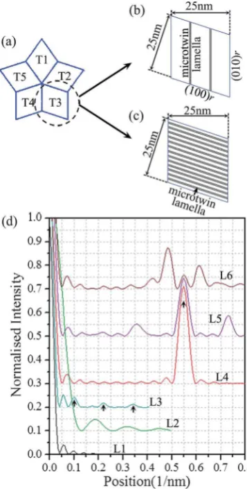
0.087 nm 1as indicated in the inset of Fig. 2f, or in other words the width of the coherently diffracting region is about 11.5 nm). This suggests that theare we have observed is not due to the coherent diffraction from the whole crystallites, but only a small fraction of the volume is involved. To mimic that, we have represented the crystallite segment with microtwin defects (shown in the cross-sectional view in Fig. 4b) by an elongated tetrahedral boron carbide crystallite with 2 layers of parallel regular-spaced {100}rmicrotwin lamellae (each lamella has 2
layers of close packing boron clusters). Given the transverse
Fig. 3 HRTEM of the T3 and T4 twinning segments of the boron carbide nanowire shown in the inset of Fig. 2c. The inset shows the corresponding diffraction pattern of the boron carbide nanowire. At this orientation, T3 and T4 are at [100]rand [010]rzone-axis diffraction conditions, respectively, while other crystalline segments (T1,
T2 and T5) are far from major zone-axis orientation and do not show atomic scale contrast in the HRTEM image.
Nanoscale Paper
Published on 05 July 2013. Downloaded by University of York on 28/08/2013 20:10:52.
[image:5.595.51.543.51.189.2]nature of the defect, we have tried to estimate the effect of partial beam coherence by adding the diffraction intensities from those defect-divided subunits either incoherently or coherently. The simulated intensity proles for both cases have been shown as L2 and L3 (Fig. 4d). We found that the intense L2 prole is more consistent with the experimental observation shown in the inset of Fig. 2f.
Theare between T2 and T3 extends further out from the respective diffraction peaks than that between T3 and T4
an intenseare with a prominent feature (indicated by black arrows in Fig. 4d) reecting the spatial periodicity of the microtwin lamellae. The comparison with the experimental case can be further improved by considering the case that the microtwin lamellae have irregular spacing. The corresponding simulated intensity distribution shows even more intenseares (L5 and L6 in Fig. 4d correspond to the models with 13 layers of irregular-spaced microtwin lamella) with more diffuse peaks. Therefore we believe that the strongare between T2 and T3 is due to the high-density irregular spaced planar defects. This prevalence of high-density parallel twins is consistent with the low stacking fault energy that is also responsible for the cyclic twinned structure in therst place.
Finally, we comment on the anisotropy of the diffraction peak broadening observed most strikingly in T3 and T4. In particular, the direction of the elongation of the T4 reection is not aligned with theare orientation, suggesting that they have a different origin. It is well known that an array of the edge dislocations, such as those present in a small angle grain boundary capable of xing the ‘extra-wedge’ problem in the boron carbide cyclic twinned nanostructure, would introduce both a tensile and a compressive strained region respectively around each core of the dislocations. This could be responsible for the anisotropic broadening of the diffraction peaks. The presence of such a small angle grain boundary is consistent with the structural model,33
where a combination of small angle grain boundary and regular microtwin array can lead to an effective solution of the strain caused by the ‘excess-wedge’ problem in boron carbide cyclic twinned nanowires.
Conclusions
In summary, we have carried out a 3D diffraction intensity reconstruction of cyclic twinned boron-rich nanowires to investi-gate their internal structures non-destructively. We have found that it is a convenient and direct method to identify the cyclic twinning structures in such nanowires. A quantitative study of the dihedral angles between the diffraction peaks reveals that heterogeneous strain distribution is the norm in nanowires of such size and none of the twinning plane remains strain-free. We expect such nanowires should be considered‘pre-strained’when discussing their mechanical responses. We have clearly identied the presence of microtwins and stacking faults, as well as the possibility for dislocation arrays. We believe that these defects, collectively, are responsible for the strain relaxation in such complex nanowires. Given its sensitivity to the microstructure of
Fig. 4 (a) The cross-sectional morphology of an idealfive-fold twinned nanowire withfive elongated tetrahedral crystalline segments labelled as T1–T5. (b) and (c)
The cross-sectional views of the proposed defective structural model of an elon-gated tetrahedral boron carbide crystallite oriented as the T3 segment in (a) with 2 and 13 layers of regular-spaced parallel {100}rmicrotwin lamellae (each lamella
has 2 layers of close packing boron clusters), respectively. The model in (b) is used to simulate the crystalline segment T3 with microtwin lamellae parallel to the twinned plane between T3 and T4. The model (c) assumes that the 13 layers of microtwin lamellae in the T3 segment are parallel to the T2–T3 twinned plane. (d)
The comparison of the simulated intensity line-profiles along the direction
perpendicular to the twinning plane. All are purely coherent simulation results except for L2 that is obtained by assuming that the intensity is the incoherent summation of the different coherent reflections from microtwin-free regions. L1 is the reference result for the idealfive-fold twinned nanowire shown in (a). L2 and L3 are for the structural model shown in (b). L4 corresponds to the structural model shown in (c). Also shown are the simulated results for structural models with 13 layers of irregular-spaced microtwin lamellae in the sequence of 1-2-3-1-2-3-1-2-3-1-2-3-2-2 (L5) and 2-2-2-1-1-1-3-3-3-2-2-2-1-3 (L6) respectively. The sequence is labelled in the unit of the {100}ratomic layer.
[image:6.595.76.255.50.403.2]the complex nanowires, the non-destructive nature of our approach is ideal for thein situstudy of nanostructured materials as a function of temperature or external action. With the rapid development of coherent electron diffraction techniques,29,30
we also expect that this approach can eventually be extended to also include electron diffraction tomography through phasing by the over-sampling method, to obtain real-space structure inversion, once such method becomes more robust in strained systems and a more coherent electron beam is used. This will allow us to study the morphology and strains within individual crystallites in real-space,20,34as well as their real-space relationship with each other. Even in its present form, our demonstration has shown that the knowledge on the 3D diffraction intensity distribution is powerful enough in revealing many hitherto unknown states of the complex nanostructure. Therefore, we expect that our current approach and its further extension into electron diffraction tomography can nd many more applications in characterization of polycrystalline materials other than the cyclic twinned nanowires.
Acknowledgements
X. Fu would like to thank National Natural Science Foundation of China for the research support (grant no. 51201015). J. Yuan would acknowledge the support of EPSRC (EP/G070474/1) and Royal Society Wolfson Foundation Laboratory Refurbishment Grant. The authors would like to thank Dr Z. Y. Yu and C. Liu for providing boron-rich nanowire samples.
Notes and references
1 L. Manna, E. C. Scher and A. P. Alivisatos,J. Am. Chem. Soc., 2000,122, 12700–12706.
2 L. D. Marks,Rep. Prog. Phys., 1994,57, 603–649.
3 Z. Y. Li, N. P. Young, M. Di Vece, S. Palomba, R. E. Palmer, A. L. Bleloch, B. C. Curley, R. L. Johnston, J. Jiang and J. Yuan,Nature, 2008,451, 46–49.
4 I. Lisiecki, A. Filankembo, H. Sack-Kongehl, K. Weiss, M. P. Pileni and J. Urban, Phys. Rev. B: Condens. Matter Mater. Phys., 2000,61, 4968–4974.
5 C. J. Johnson, E. Dujardin, S. A. Davis, C. J. Murphy and S. Mann,J. Mater. Chem., 2002,12, 1765–1770.
6 S.-H. Zhang, Z.-Y. Jiang, Z.-X. Xie, X. Xu, R.-B. Huang and L.-S. Zheng,J. Phys. Chem. B, 2005,109, 9416–9421. 7 J. Jiang, M. H. Cao, Y. K. Sun, P. W. Wu and J. Yuan,Appl.
Phys. Lett., 2006,88, 163107.
8 X. Fu, J. Jiang, C. Liu and J. Yuan,Nanotechnology, 2009,20, 365707.
9 A. Guerrero-Mart´ınez, S. Barbosa, I. Pastoriza-Santos and
L. M. Liz-Marz´an, Curr. Opin. Colloid Interface Sci., 2011, 16, 118–127.
10 C. P. Li, C. S. Lee, X. L. Ma, N. Wang, R. Q. Zhang and S. T. Lee,Adv. Mater., 2003,15, 607–609.
11 H. Y. Chen, Y. Gao, H. R. Zhang, L. B. Liu, H. C. Yu, H. F. Tian, S. S. Xie and J. Q. Li, J. Phys. Chem. B, 2004, 108, 12038–12043.
12 B. Wu, A. Heidelberg, J. J. Boland, J. E. Sader, X. M. Sun and Y. D. Li,Nano Lett., 2006,6, 468–472.
13 T. Filleter, S. Ryu, K. Kang, J. Yin, R. A. Bernal, K. Sohn, S. Li, J. Huang, W. Cai and H. D. Espinosa,Small, 2012,8, 2986– 2993.
14 M. Song, A. Bouhelier, P. Bramant, J. Sharma, E. Dujardin, D. Zhang and G. Colas-des-Francs, ACS Nano, 2011, 5, 5874–5880.
15 P. A. Midgley and R. E. Dunin-Borkowski,Nat. Mater., 2009, 8, 271–280.
16 I. Arslan, J. R. Tong and P. A. Midgley,Ultramicroscopy, 2006, 106, 994–1000.
17 U. Kolb, T. Gorelik, C. K¨ubel, M. T. Otten and D. Hubert, Ultramicroscopy, 2007,107, 507–513.
18 U. Kolb, T. Gorelik and M. T. Otten,Ultramicroscopy, 2008, 108, 763–772.
19 E. Mugnaioli, T. Gorelik and U. Kolb,Ultramicroscopy, 2009, 109, 758–765.
20 R. Dronyak, K. S. Liang, J.-S. Tstai, Y. P. Stetsko, T.-K. Lee and F.-R. Chen,Appl. Phys. Lett., 2010,96, 221907.
21 H. Hofmeister, in Encyclopedia of Nanoscience and
Nanotechnology, ed. H. S. Nalwa, American Scientic
Publishers, 2004, pp. 431–452.
22 V. G. Gryaznov, J. Heydenreich, A. M. Kaprelov, S. A. Nepijko, A. E. Romanov and J. Urban,Cryst. Res. Technol., 1999,34, 1091–1119.
23 Z. Guan, T. Gutu, J. Yang, Y. Yang, A. A. Zinn, D. Li and T. T. Xu,J. Mater. Chem., 2012,22, 9853–9860.
24 X. Lin and P. Darrell Ownby,J. Mater. Sci., 2000,35, 411–418. 25 V. I. Matkovich,Boron and refractory borides, Springer-Verlag,
Berlin, 1977.
26 H. Zheng, J. Wang, J. Y. Huang, A. Cao and S. X. Mao,Phys. Rev. Lett., 2012,109, 225501.
27 B. G. Bagley,Nature, 1965,208, 674–675.
28 R. De Wit,J. Phys. C: Solid State Phys., 1972,5, 529–534. 29 W. J. Huang, R. Sun, J. Tao, L. D. Menard, R. G. Nuzzo and
J. M. Zuo,Nat. Mater., 2008,7, 308–313.
30 W. J. Huang, J. M. Zuo, B. Jiang, K. W. Kwon and M. Shim, Nat. Phys., 2009,5, 129–133.
31 J. Reyes-Gasga, A. G´omez-Rodr´ıguez, X. Gao and M.
Jos´e-Yacam´an,Ultramicroscopy, 2008,108, 929–936.
32 Z. Yu, J. Jiang, J. Yuan and J. Zhu,J. Cryst. Growth, 2010,312, 1789–1792.
33 X. Fu, J. Jiang, W. Zhang and J. Yuan,Appl. Phys. Lett., 2008, 93, 043101.
34 V. Favre-Nicolin, F. Mastropietro, J. Eymery, D. Camacho, Y. M. Niquet, B. M. Borg, M. E. Messing, L.-E. Wernersson, R. E. Algra, E. P. A. M. Bakkers, T. H. Metzger, R. Harder and I. K. Robinson,New J. Phys., 2010,12, 035013.
Nanoscale Paper
Published on 05 July 2013. Downloaded by University of York on 28/08/2013 20:10:52.