This is a repository copy of The increase of the spin-transfer torque threshold current density in coupled vortex domain walls.
White Rose Research Online URL for this paper: http://eprints.whiterose.ac.uk/43877/
Article:
Lepadatu, S, Mihai, AP, Claydon, JS et al. (5 more authors) (2012) The increase of the spin-transfer torque threshold current density in coupled vortex domain walls. Journal of Physics: Condensed Matter, 24 (2). 024210 - ? . ISSN 0953-8984
https://doi.org/10.1088/0953-8984/24/2/024210
[email protected] https://eprints.whiterose.ac.uk/ Reuse
See Attached
Takedown
If you consider content in White Rose Research Online to be in breach of UK law, please notify us by
Increase of spin-transfer torque threshold current density in
coupled vortex domain walls
S. Lepadatu1, A.P. Mihai1, J.S. Claydon1, F. Maccherozzi2, S.S. Dhesi2, C.J. Kinane3,
S. Langridge3 and C.H. Marrows1
1School of Physics and Astronomy, E.C. Stoner Laboratory, University of Leeds, Leeds LS2 9JT,
United Kingdom
2Diamond Light Source, Chilton, Didcot OX11 0DE, United Kingdom
3ISIS, Rutherford Appleton Laboratory, Chilton, Didcot OX11 0QX, United Kingdom
Abstract:
We have studied the dependence on domain wall structure of the spin-transfer
torque current density threshold for the onset of wall motion in curved, Gd-doped
Ni80Fe20 nanowires with no artificial pinning potentials. For single vortex domain
walls, both for 10% and 1% Gd doping concentrations, the threshold current density is
inversely proportional to the wire width and significantly lower compared to the
threshold current density measured for transverse domain walls. On the other hand for
high Gd concentrations and large wire widths, double vortex domain walls are formed
which require an increase in the threshold current density compared to single vortex
domain walls at the same wire width. We suggest that this is due to the coupling of
the vortex cores, which are of opposite chirality, and hence will be acted on by
Current-induced domain wall motion is being actively pursued as a basis for
the operation of magnetic memory devices such as race-track memory [1] and
magnetic logic [2]. The main difficulty stems from the large current densities required
for the operation of such devices, which results in rapid degradation and eventual
failure due to electromigration and accumulated damage from heating. As the domain
wall is initially at rest the local pinning must be overcome in order for current-induced
domain wall motion to be initiated. Two types of local pinning may be distinguished,
intrinsic pinning arising from material properties alone such as hard axis anisotropy
[3] and extrinsic pinning due to artificially created pinning potentials [4,5] or defects
such as edge roughness [6,7]. Methods of reducing the threshold current density have
been investigated, including resonant excitation of domain walls [8] in wires with no
pinning potentials [9] as well as wires with artificial pinning potentials [10,11], and
modification of material parameters by addition of dopant concentrations [12].
We have previously studied the threshold current density required for domain
wall depinning from artificial pinning potentials, where the extrinsic pinning
dominates the intrinsic pinning [4]. Here we study the opposite case where the sources
of extrinsic pinning are minimized in order to characterize the dependence of the
intrinsic pinning on domain wall structure and material parameters. This problem is
addressed here for double vortex structures: coupled pairs of vortex domain walls
Smoothly curved L-shaped nanowires have been fabricated on highly resistive
Si/SiO2 substrates using electron beam lithography with varying width from 2 m
down to 200 nm. The wires have pointed ends to suppress domain wall formation at
either end. Gd doped Ni80Fe20 (Py) was sputtered from stoichiometric targets with 1 %
and 10 % Gd concentration, 10 nm thick, and the wires were obtained using lift-off. A
second electron beam lithography step was used to define the Ti (10 nm) / Au (50 nm)
electrical leads as shown in the inset to Fig. 1(a), whilst the main contact pads were
defined using optical lithography and sputtering of Ti (10 nm) / Au (120 nm). The
current injection and voltage measurement configuration is also shown in the inset to
Fig. 1(a). The current injection pads were connected to a voltage pulser using
impedance matched probes, whilst the wire resistance was measured using a lock-in
amplifier method. External magnetic fields were applied in the direction indicated in
Fig. 1(b), slightly offset from the direction that bisects the wire corner.
A typical magneto-resistance (MR) response of a curved wire is shown in Fig.
1(a) with the main magnetization configuration states labelled A through D on the
positive-going field sweep (symmetrically equivalent states are to be found on the
negative-going sweep). Micromagnetic simulations of these states, obtained using the
OOMMF code [13], are shown in Fig. 1(b). In state A the magnetization in the wire is
almost saturated by a large negative field across its width in the region between the
voltage probes, resulting in a minimum resistance due to the anisotropic MR effect
(AMR). Relaxing the magnetic field to zero results in domain wall formation in the
curved section of the wire at zero field, state B, owing to the shape anisotropy of the
wire which forces the magnetization to align along the length of the wire in opposite
the wire—all but for the domain wall—now has its magnetization lying parallel to the
current path. The application of a positive magnetic field switches the wire into a
single domain, state C, with the domain wall travelling through the right-hand side
section of the wire under the action of the magnetic field. State C' is a snapshot of this
process occurring. This results in a small but sharp increase in resistance due to the
AMR effect as the wall is expelled, just before state C is achieved. A slight deviation
of 5º from the perpendicular direction of the magnetic fields has been used, as shown
in Fig. 1(a), to result in reproducible domain wall motion towards the right. A further
sharp increase in resistance is observed just prior to obtaining state D, as the magnetic
field is increased resulting in coherent magnetization rotation of the left section of the
wire. This aligns the magnetic moments of that section more closely to the wire axis,
and thus more parallel to the current flow, due to shape anisotropy, resulting in an
overall increase in resistance due to AMR. For a large enough magnetic field the wire
Figure 1 – (colour online) (a) Magnetoresistance for a curved wire (200 nm wide,
Py99Gd1) and (b) micromagnetic simulations showing the magnetization switching
steps. In the inset of (a) the electrical contact configuration is shown. State A is at
saturation, state B at zero field with a domain wall formed, state C is the single
domain state after the domain wall is expelled out of the right arm, with C’ occurring
during this process, and state D is obtained after coherent rotation of magnetization in
the left arm. The dotted and dashed lines indicate the switching fields for domain wall
motion and coherent rotation respectively, which may easily be determined by AMR
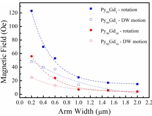
[image:6.595.185.413.66.432.2]The variation in the two switching fields – domain wall motion for right arm
switching and coherent magnetization rotation for left arm switching – is shown in
Fig. 2 as a function of arm width for both Gd-doping concentrations. As expected, due
to the decrease in arm width, both the domain wall motion and magnetization rotation
switching fields increase [14]. On the other hand the switching fields are significantly
reduced for the larger Gd concentration, owing to the reduction in net magnetic
moments with Gd doping, which we have measured previously, as the switching field
is dominated by the shape anisotropy [15], which is in turn proportional to the square
[image:7.595.170.425.344.539.2]of the magnetization.
Figure 2 – (colour online) Switching fields measured by AMR as a function of arm
width and Gd concentration. The lines are guides for the eye.
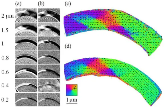
The remanent domain wall structure (state B) was investigated by means of
x-ray magnetic circular dichroism photo-emission electron microscopy (PEEM)
imaging with the I06 beamline at the Diamond Light Source synchrotron. Imaging
was carried out at near zero field (less than 1 Oe), after saturation in 700 Oe.
absorption edges have been used. By obtaining two PEEM images with the x-ray
beam angle with respect to the sample in orthogonal directions a vector map of the
magnetization is obtained, as explained previously [10]. Images of the domain wall
structures as a function of wire width and Gd concentration are shown in Fig. 3. For
the 200 nm wire width we find transverse domain walls are formed, in agreement with
previous calculations of the domain wall phase diagram in Py [16]. For the wider
wires we observe single vortex domain wall formation, with the exception of the 1.5
m and 2 m wide Py90Gd10 wires for which we observe a remarkable double vortex
domain wall structure. The double vortex domain wall consists of two coupled vortex
structures with opposite chiralities as shown in Fig. 3(c). As we have previously
found, Gd doping of permalloy increases the out-of-plane anisotropy [15]. This results
in lower energy cost of supporting a vortex core, which may explain the formation of
double vortex domain walls for the larger Gd concentration.
Figure 3 – (colour online) PEEM images of domain wall structure as a function of
wire width and Gd concentration, (a) 1 % Gd concentration and (b) 10 % Gd
concentration with the exception of the 200 nm wide wire which has 2.5 % Gd
concentration. (c) and (d) PEEM vector maps of 2 m and 1.5 m wide Py90Gd10
[image:8.595.172.462.429.617.2]We next investigate the effect of domain wall structure and wire width on the
threshold current density for current-induced domain wall motion. For these
measurements we first form a domain wall between the voltage measurement leads by
saturating with a large magnetic field (-700 Oe) and then setting the field to zero.
Following domain wall formation a series of voltage pulses (~2000) of controlled
height and fixed duration of 70 ns was injected between the outer current injection
leads resulting in electron flow direction towards the right injection lead – see inset to
Fig. 1(a). A large number of pulses with a short duration was chosen so as to
minimize the risk of wire damage over repeated measurements due to excessive
heating, whilst still having a sufficiently long time to completely remove the domain
wall. We also performed measurements with longer current pulses (50 µs) and
obtained the same values of threshold current. Following voltage pulse injection the
depinning of domain walls from between voltage measurement leads was tested by
measuring the MR response of the wires on returning to the negative starting field, as
shown in Fig. 4. For small voltage pulse heights, where the domain wall remains
between the voltage measurement leads, a smooth decrease in resistance is measured
with increasing magnetic field intensity as the wire gradually reverses from state B to
state A. For large enough voltage pulse heights to remove the domain wall from
between the voltage measurement leads, generating state C, (in addition to a small
initial increase in resistance due to the removal of the AMR contribution of the
domain wall) a switching event is measured as the wire switches into state D at the
magnetic field corresponding to magnetization rotation in the right arm, as shown in
Fig. 4. We use the latter method to detect removal of the domain wall as it is more
reliable than simply measuring the resistance at zero field following voltage pulse
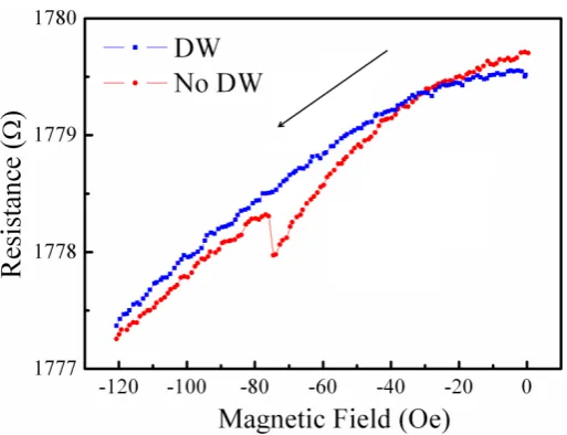
Figure 4 – (colour online) Domain wall movement detection method. If the DW
remains in the corner of the wire it can smoothly return to a saturated state, whilst if it
was ejected by the current pulse a new wall has to be created and annihilated to reach
saturation, leading to a step-like feature in the magnetoresistance response.
The results are summarised in Fig. 5, showing the variation of threshold
current density with arm width for the two different Gd concentrations. We group the
DWs by their topology, as determined from the PEEM imaging. The threshold current
densities for transverse walls are larger compared to those for vortex walls in
agreement with previous reported work [17]. For vortex domain walls the threshold
current density decreases as the arm width is increased for both Py99Gd1 and Py90Gd10.
In the absence of pinning potentials, for large domain walls in the purely adiabatic
limit where the spin transfer mechanism dominates as is the case here, i.e. domain
wall width >> F, where F is the Fermi wavelength, the threshold current density jTH
[image:10.595.171.428.95.292.2] K a eS j
3 2 TH ,
where a is the lattice constant and S the magnitude of the localized spin. For
transverse domain walls the threshold current is set by the hard axis in-plane
anisotropy with the edge roughness contributing a further increase of the threshold
current due to extra pinning [17]. For the 200 nm wide Py99Gd1 and Py90Gd10 wires,
the contribution from edge roughness pinning is expected to be equal. Since for a
planar wire the hard axis anisotropy is set by the shape anisotropy, the reduction in net
magnetic moment for Py90Gd10 compared to Py99Gd1 [15] explains the lower
[image:11.595.171.427.395.589.2]threshold current measured for Py90Gd10.
Figure 5 – (colour online) Threshold current density as a function of arm width and
Gd concentration. Circles are for Py90Gd10 and squares for Py99Gd1. A fit using Eq. 2
to the vortex domain walls for Py99Gd1 is also shown as the solid line.
For vortex domain walls, since the vortex core magnetization is perpendicular
to the sample plane, the threshold current is set by the out-of-plane hard axis
anisotropy [3]. We have previously measured an increase in the out-of-plane
anisotropy field with Gd doping [15] leading to a decrease in the energy required to
support a vortex core, resulting in lower threshold currents for Py90Gd10 vortex
domain walls compared to Py99Gd1. As shown by Heyne et al. [18] the threshold
current density required for continuous motion of a vortex wall is connected to the
energy cost of creating a vortex-antivortex pair at the wire edges. Since ≠ , where
is the Gilbert damping and is the non-adiabaticity parameter, as the vortex domain
wall is displaced the vortex core attains a transverse displacement dependent on its
polarity. As the vortex core reaches the wire edge a vortex-antivortex pair is nucleated
with opposite polarity and the antivortex annihilates with the original vortex. This
process leaves behind a single vortex core with reversed polarity which is now able to
move towards the opposite wire edge as the whole vortex domain wall is displaced
along the wire [18]. The energy cost of creating the vortex-antivortex pair depends on
the out-of-plane anisotropy and results in an inverse dependence of threshold current
density on wire width W according to [18]
0 3 2 v 0 W TH 2 j W K a d e j j
j
,
where dv is the vortex core size (~10 nm). A further contribution to the threshold
current density, termed j0, must be included in order to reproduce the results shown in
Fig. 5 for vortex domain walls, as the measured threshold current densities do not
There are not enough data points in any one group to do a quantitative fit to the data
for the Py99Gd10 samples, but the value of j0 does not seem to be very different for
these nanowires from the overall trend in the data. The origin of this offset threshold
current density is most likely to be the weak pinning resulting from edge roughness
and magnetic non-uniformity which cannot be completely eliminated in real systems.
Note that we obtain the same values of threshold currents when repeating the
measurements with single voltage pulses of much longer duration of 70 s, as the
critical point which needs to be overcome to sustain continuous domain wall motion
is the creation of the vortex-antivortex pair which requires the largest current density.
Thus for the start-stop measurements using the shorter 70 ns pulses the domain wall
will also be completely removed from between the voltage measurement pads
provided the initial current density is large enough to overcome the threshold required
for vortex-antivortex pair creation. We also note that the shorter 70 ns pulse duration
is long enough to avoid the oscillatory dynamical effects observed at shorter pulse
durations. [9]
We now analyse the case of the double vortex domain walls present in the 1.5
and 2 m wide Py90Gd10 wires. In contrast to the Py99Gd1 wires, larger threshold
currents are measured for the double vortex domain walls, roughly two times larger,
as shown in Fig. 5. This stands in contrast to the dependence of domain wall
propagation fields on wire width and Gd doping in Fig. 2, showing that extrinsic
pinning due to edge roughness and magnetic non-uniformity cannot alone explain the
results shown in Fig. 5. On the other hand, the mechanism of vortex-antivortex pair
creation may be used to understand the larger threshold currents required to fully
vortex cores undergo a transverse displacement towards the wire edges and reverse
polarity following creation of vortex-antivortex pairs and annihilation with the
original vortex cores. For the double vortex wall, effectively a system of two coupled
vortices with opposite chiralities, the energy required to create two vortex-antivortex
pairs is increased by at least a factor of two, resulting in an increase of the threshold
current density. Note that we expect the threshold current density for two vortex
domain walls sufficiently far apart to revert back to Eq. 2 as the motion of the two
vortex cores becomes independent.
Finally we discuss the effect of non-adiabaticity. The non-adiabatic
spin-transfer torque is introduced into the Landau-Lifshitz-Gilbert equation as a second
order modification to the purely adiabatic spin-transfer torque, and is directly
proportional to the spin-flip scattering rate [6]. For steady-state domain wall motion,
below Walker breakdown the domain wall velocity, v, is given by vu/where
S B/ eM2 JPg
u with P being the current spin-polarization, J the current density
and MS the saturation magnetization. Thus for a perfect wire and > 0, steady domain
wall movement may be sustained at arbitrarily small current densities. Thiaville et al.
[6] have shown that if imperfections are introduced, a threshold current density is
required for steady domain wall movement, which decreases as is increased. We
have previously shown that Gd doping of Py results in increased values of [12]
which in the present case should result in decreased threshold current density due to
extrinsic pinning, namely j0. On the other hand the increase in does not affect the
In conclusion, by varying the wire width and Gd doping of Py we have studied
the dependence of threshold current density on domain wall structure and material
parameters. In all cases the threshold current density may be separated in two
contributions, one arising from intrinsic pinning due to the hard axis anisotropy and
the other from extrinsic pinning due to pinning potentials resulting from
imperfections. The threshold current density arising from intrinsic pinning is inversely
dependent on wire width for vortex domain walls and is more than doubled for
systems of two coupled vortex walls. On the other hand the threshold current density
arising from extrinsic pinning is independent of wire width and inversely proportional
to the non-adiabaticity parameter.
This research was supported by the UK EPSRC. We are grateful to the Diamond
References
1
S.S.P. Parkin, M. Hayashi, L. Thomas, Science 320, 190, (2008)
2
P. Xu, K. Xia, C. Gu, L. Tang, H. Yang, J. Li, Nature Nanotech. 3, 97 (2008)
3
G. Tatara, H. Kohno, Phys. Rev. Lett. 92, 086601 (2004)
4
S. Lepadatu, A. Vanhaverbeke, D. Atkinson, R. Allenspach, C.H. Marrows, Phys.
Rev. Lett. 102, 127203 (2009)
5
D. Bedau, M. Kläui, S. Krzyk, U. Rüdiger, G. Faini, L. Vila, Phys. Rev. Lett. 99,
146601 (2007)
6
A. Thiaville, Y. Nakatani, J. Miltat and Y. Suzuki, Europhys. Lett. 69, 990 (2005)
7
M. Kläui, P.-O. Jubert, R. Allenspach, A. Bischof, J.A.C. Bland, G. Faini, U.
Rüdiger, C.A.F. Vaz, L. Vila, C. Vouille, Phys. Rev. Lett. 95, 026601 (2005)
8
E. Saitoh, H. Miyajima, T. Yamaoka, G. Tatara, Nature (London) 432, 203 (2004)
9
L. Thomas, M. Hayashi, X. Jiang, R. Moriya, C. Rettner, S.P. Parkin, Nature
(London) 443, 197 (2006)
10
S. Lepadatu, J.S. Claydon, C.J. Kinane, T.R. Charlton, S. Langridge, A. Potenza,
S.S. Dhesi, P.S. Keatley, R.J. Hicken, B.J. Hickey, C.H. Marrows, Phys. Rev. B 81,
060402 (2010)
11
R. Moriya, L. Thomas, M. Hayashi, Y.B. Bazaliy, C. Rettner, S.P. Parkin, Nat.
Phys. 936 (2008)
12
S. Lepadatu, J.S. Claydon, D. Ciudad, A. Naylor, C.J. Kinane, S. Langridge, S.S.
Dhesi, C.H. Marrows, Appl. Phys. Exp. 3, 083002 (2010)
13
M.J. Donahue and D.G. Porter, OOMMF User's Guide, Version 1.0, Interagency
Report NISTIR 6376, National Institute of Standards and Technology, Gaithersburg,
MD (Sept 1999).
14
15
S. Lepadatu, J.S. Claydon, D. Ciudad, C.J. Kinane, S. Langridge, S.S. Dhesi, C.H.
Marrows, Appl. Phys. Lett. 97, 072507 (2010)
16
Y. Nakatani, A. Thiaville, J. Miltat, J. Magn. Magn. Mater. 290, 750 (2005)
17
L. Heyne, M. Kläui, D. Backes, T.A. Moore, S. Krzyk, U. Rüdiger, L.J.
Heyderman, A.F. Rodriguez, F. Nolting, T.O. Mentes, M.Á. Niño, A. Locatelli, K.
Kirsch and R. Mattheis, Phys. Rev. Lett. 100, 066693 (2008)
18
L. Heyne, J. Rhensius, Y.-J. Cho, D. Bedau, S. Krzyk, C. Dette, H.S. Körner, J.
Fischer, M. Laufenberg, D. Backes, L.J. Heyderman, L. Joly, F. Nolting, G. Tatara, H.