On-chip GaN-based dual-color micro-LED arrays
and their application in visible light
communication
J. F. C. C
ARREIRA,
1,3,4E. X
IE,
1,3,5R. B
IAN,
2,3C. C
HEN,
2J. J.
D. M
CK
ENDRY,
1B. G
UILHABERT,
1H. H
AAS,
2E. G
U,
1 ANDM. D. D
AWSON11Institute of Photonics, Department of Physics, University of Strathclyde, Glasgow G1 1RD, UK 2Institute for Digital Communications, Li–Fi R&D Centre, University of Edinburgh, Edinburgh EH9 3JL,
UK
3These authors contributed equally to this work 4[email protected]
Abstract: Integrated multi-color micron-sized light emitting diode (micro-LED) arrays have been demonstrated in recent years for display applications; however, their potential as visible light communication (VLC) transmitters is yet to be fully explored. In this work, we report on the fabrication and characterization of on-chip dual-color micro-LED arrays and their application in VLC. For this purpose, blue-green and blue-violet micro-LED arrays were fabricated by transfer printing blue-emitting micro-LEDs onto the substrate of green and violet micro-LEDs, respectively. The potential of these dual-color micro-LED arrays as VLC transmitters is demonstrated with respective error-free data rates of 1.79 and 3.35 Gbps, achieved by the blue-green and blue-violet devices in a dual wavelength multiplexing scheme.
Published by The Optical Society under the terms of theCreative Commons Attribution 4.0 License. Further distribution of this work must maintain attribution to the author(s) and the published article’s title, journal citation, and DOI.
1. Introduction
The interest in gallium nitride (GaN)-based micron-sized light emitting diodes (micro-LEDs), of lateral dimension smaller than 100 µm, has increased dramatically in recent years [1]. GaN-based micro-LEDs offer exceptional brightness, contrast, fast response time, long operation lifetime, and low power consumption, which have facilitated their application in several fields, such as microdisplays [2–4], visible light communication (VLC) [5,6], fluorescence sensing [7], and optoelectronic tweezing [8]. Despite the huge success of monochromatic GaN-based micro LED with different configurations for the aforementioned applications, a general thread common to many applications is the desire for different color micro-emitters on a single chip platform. Multi-color emission can be achieved by using color converters to downshift the GaN-based micro-LED blue emission to longer wavelengths. However, due to the color converters’ lower efficiency, slow response time, and short lifespan, this solution is unsuitable for many applications [3]. Although possible [9–11], the growth of highly efficient inorganic red, green, and blue emitting materials on a single wafer is still in its early stages and is extremely challenging. As, currently, highly efficient blue and green emitting LED structures are GaN-based, while efficient red emitters are aluminum gallium indium phosphide-based [12]. An alternative is to fabricate blue, green, and red emitting micro-LEDs on their respective growth wafers and then transfer the three different color emitting micro-LEDs onto a common substrate. Conventional assembly techniques, relying on robotic systems for placement of materials mechanically diced from a source wafer onto a common platform, are incapable of handling ultrasmall micro-LEDs
#369065 https://doi.org/10.1364/OE.27.0A1517
[13]. This has pushed research into strategies of suspending releasable ultrathin micro-LED platelets (still tethered to their growth substrate) and subsequent assembly by transfer printing (TP) techniques [13,14]. Following this approach, several reports of TP-enabled multi-color inorganic micro-LED arrays, targeting microdisplay applications, have emerged [15–17].
To the best of our knowledge, however, the potential of on-chip multi-color inorganic micro-LED arrays as VLC transmitters has not yet been fully explored. Monochromatic GaN-based micro-LEDs have been successfully demonstrated as multi-Gbps VLC transmitters [18–20]. Their success has been attributed to their hundreds of MHz -6 dB electrical modulation bandwidth combined with spectrally efficient modulation schemes, such as orthogonal frequency division multiplexing (OFDM) [19]. Furthermore, the communication capacity can be increased by using different color emitting micro-LEDs and wavelength division multiplexing (WDM) techniques. This concept has been successfully implemented in a multi-Gbps VLC link using separate micro-LED chips of different colors [21]. But where the micro-LED transmitters were spatially separated by 10’s of cm and optics were required for efficient color mixing.
In this work, we report the fabrication, characterization, and VLC application of transfer printing-enabled on-chip GaN-based blue-green and blue-violet micro-LED arrays. In section 2, we present the micro-LED fabrication process on their growth substrates and subsequent integration of the blue emitting micro-LEDs, onto the green or violet micro-LED substrate by transfer printing. In section3, firstly the electrical, optical, and bandwidth performance of individual violet, green, and blue micro-LEDs are shown; secondly the color mixing properties of the blue-green and blue-violet micro-LED arrays are presented in terms of their color coordinates; finally the capability of the blue-green and blue-violet micro-LED arrays as VLC transmitters in two different WDM experimental set-ups (with and without a dichroic mirror) is demonstrated with Gbps error free data rates achieved by respective pairs of micro-LEDs. These results show the potential for micro-LED arrays that act both as a display and as a high-speed VLC transmitter.
2. Device fabrication
2.1. Violet and green micro-LEDs based on GaN-on-sapphire epitaxy
Violet and green emitting (405 nm and 520 nm, respectively) micro-LEDs in flip-chip configuration were fabricated from commercial InGaN epistructures, grown on c-plane patterned sapphire substrate (PSS), following previously reported microfabrication procedures [20]. The violet LED epitaxial structure consisted of a 4.5 µm GaN buffer layer, a 1.8 µm thick n-doped GaN, an 116 nm thick active layer, a 85 nm magnesium-doped aluminum gallium nitride (AlGaN:Mg) cladding layer, and finally a 25 nm thick p-doped GaN layer. The green LED epitaxial structure consisted of a 3 µm undoped GaN buffer layer, 4 µm of n-doped GaN, a 130 nm thick active layer, and was topped with a 300 nm thick p-doped GaN layer. In the first fabrication step, a p-GaN metal contact (Palladium (Pd), thickness 100 nm) was electron-beam deposited, lithographically patterned, and annealed in a nitrogen environment at 300 °C. Inductively coupled plasma (ICP) etching was used to expose the underlying n-GaN layer defining a 20 µm diameter pixel (3.15×10⁻⁶cm2active area). Another ICP etch step created a 90 µm side square mesa down to the PSS, thus further reducing the micro-LEDs capacitance [19]. Then, a metal sputter deposition (Titanium (Ti)/Gold (Au), thicknesses 50/200 nm) defined the n-GaN metal contact layer. Next, a 300 nm silicon dioxide (SiO2) passivation layer was deposited by plasma-enhanced chemical vapor deposition
(PE-CVD) and a SiO2aperture on top of the p-GaN was defined by reactive ion etching (RIE).
Finally, a second Ti/Au metallization step defined the metal track.
2.2. Blue micro-LED platelets from a GaN-on-silicon wafer
epitaxial structure consisted of a 200 nm thick aluminum nitride (AlN) layer, followed by a 650 nm Al-graded GaN buffer layer, a 300 nm non-intentionally doped GaN layer, an 800 nm thick n-doped GaN, an 100 nm thick active layer, and an 140 nm thick p-doped GaN layer. An L-shaped pixel (active area of 6.5×10⁻⁵cm2) and a 100 µm squared mesa were defined by the same processes as for the violet and green micro-LEDs. The blue TP micro-LED pixel size was chosen to be larger than the violet and green micro-LEDs in order to compensate for its lower optical power density. Additionally, in order to yield transferable micro-LED platelets, the following steps were undertaken. First, supporting “anchors”, that tether the micro-LED platelet to the growth substrate, were defined during the ICP mesa etching. Second, an additional etching step was used to expose the chemically preferentially etched Si(110) planes. Third, by wet etching (30% potassium hydroxide (KOH) solution at 80 °C) the Si(110) planes underneath the micro-LED platelets were removed. Upon completion of the underetch step, the blue micro-LED platelets are held suspended, above an air gap (2 µm), by the two diagonally opposed sacrificial anchors [22].
2.3. Dual-color micro-LED arrays integrated by transfer printing
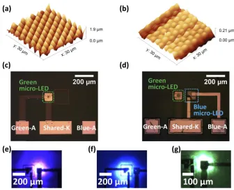
Fig. 1.Atomic force microscopy image of the PSS (a) before and (b) after SU-8 coating; plan-view optical micrograph of the blue-green micro-LED array (c) before and (d) after transfer printing of the blue micro-LED platelet. A and K are the respective anode and common cathode contact pads. Plan-view optical micrograph of the (e) violet, (f) blue, and (g) green micro-LEDs individually driven at the current density of 318 A/cm2, 15 A/cm2, and 318 A/cm2, respectively.
3. Device performance and application
3.1. Electrical, optical and bandwidth performance of single-color micro-LEDs
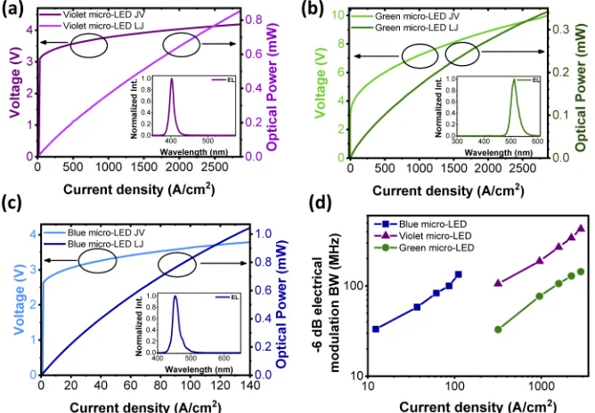
The room-temperature (RT) current density – voltage (J-V) and optical power – current density (L-J) performance of the violet, green, and blue micro-LEDs fabricated in this work are shown in Figs.2(a)–2(c), respectively. In addition, the electroluminescence (EL) spectra of each single-color micro-LED, acquired at value of current density of 318 A/cm2for the violet and green
micro-LEDs and 15 A/cm2for the blue micro-LED, are also presented. The J-V characteristic
value is lower than the one achieved by a similar device employing SU-8 as insulation layer, which demonstrates the superior capability of parylene-C as an electrical insulation layer for these TP micro-LEDs. In addition, the low reverse leakage current is also a good indicator of the excellent JV performance shown by the TP micro-LED.
[image:5.612.140.474.285.517.2]The RT -6 dB electrical modulation bandwidths of the micro-LEDs with different colors were measured by applying a DC bias combined with a small-signal modulation from an HP8753ES network analyzer. The optical response was collected by a lens system and focused onto a fast photodiode (Femto HAS-X-S-1G4-SI bandwidth 1.4 GHz). The -6 dB electrical modulation bandwidths of each micro-LED, at different current densities, are shown in Fig.2(d). The violet and green micro-LEDs exhibit the -6 dB electrical bandwidth up to 427 MHz and 144 MHz, respectively. The lower bandwidth and optical power of the green micro-LED, when compared to the violet micro-LED, can be attributed to its higher In content in the active region, and thus stronger quantum confined stark effect [26]. Furthermore, the transfer printed blue micro-LED shows a -6 dB electrical bandwidth up to 134 MHz. The lower value achieved by this micro-LED is related to its larger size and, thus, lower current density operation.
Fig. 2.(a), (b), and (c) Violet, green, and blue micro-LEDs current density-voltage curve, current density-optical power curve, and electroluminescence spectra, respectively; (d) Violet, green, and blue micro-LEDs -6 dB electrical modulation bandwidth as a function of the current density.
3.2. Color properties of dual-color micro-LED arrays
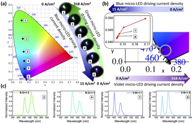
CIE1931 color coordinates of the blue-green and blue-violet micro-LED array on the color space chromaticity diagram are shown in Figs.3(a) and3(b), respectively. For the blue-green array, by increasing the current density of the blue micro-LED from 0 to 15 A/cm2and simultaneously
decreasing the current density of the green micro-LED from 318 to 0 A/cm2, it is possible to
conditions. The slightly violet appearance of the blue micro-LED, at 15 A/cm2, is a digital artifact due to the photographic camera detector. On the other hand, for the blue-violet array, varying the driving current of both micro-LEDs results in a small change of the CIE color coordinates. The enlarged inset shows, in further detail, how indistinguishable the CIE color coordinates of blue-violet array at different biases are. This is due to the poorer human eye response in the violet-blue region, when compared to blue-green spectral region [27]. The typical blue-green and blue-violet array EL spectra, at different integrated area ratios of blue-green and blue-violet, respectively, correspond to the superposition of the individual spectra of each light source, as shown in Fig.3(c).
Fig. 3.(a) Blue-green micro-LED array CIE1931 coordinates on the CIE1931 color space chromaticity diagram and photographs of the device at different biases; (b) blue-violet micro-LED array CIE1931 color coordinates at different biases; (c) electroluminescence spectra from the blue-green and blue-violet array at different integrated area ratios of blue-green and blue-violet, respectively.
3.3. VLC application of dual-color micro-LED arrays in WDM mode
The light transmitted through the dichroic mirror was focused onto an optical receiver and the light reflected by the dichroic mirror was focused onto another optical receiver. Bandpass filters were also placed in front of the detectors in order to minimize crosstalk. This set-up enabled simultaneous reception of both channels, though the use of the dichroic mirror leads to signal power losses. The distance between transmitter and detector was kept at 30 cm, in both set-ups and throughout the measurements.
Fig. 4.Schematic drawing of the experimental set-ups in wavelength division multiplexing data transmission experiments: (a) set-up 1 (WDM1); (b) set-up 2 (WDM2). The photograph inset in the schematics is the actual blue-green micro-LED array (wire bonded to a printed circuit board - PCB) being operated in WDM mode.
the light emitted by the dual-color micro-LED array was focused onto a p-i-n photodetector (New Focus 1601AC) by using an aspheric condenser lens (ACL4532). The signal from the photodetector was captured by an oscilloscope (Keysight MSO7104B) and sent back to the PC for demodulation. In order to maximize the achievable data rate, a bit and energy loading algorithm [18] was applied. Therefore, the signal-to-noise ratio (SNR) on each subcarrier was estimated at the beginning of the communication performance measurement. Based on the estimated SNR and a bit-error-ratio (BER) target that is acceptable for the application of forward error correction (FEC) coding, modulation order and symbol energy on each subcarrier was calculated. Finally, the signals with bit and energy loading were transmitted and the achieved data rate and BER were measured.
3.4. Communication performance of the blue-green micro-LED array
[image:8.612.142.470.334.584.2]The results of the blue-green micro-LED array operated in a WDM mode with different set-ups are summarized in Fig.5. The blue and green micro-LEDs were operated at 138 A/cm2and 2.8 kA/cm2, respectively, whilst the modulation signal peak-to-peak voltage was set to 1.5 V, after the amplifier. The sampling frequency was set as 16 GSa/s and number of samples per symbol was optimized for each link. The SNR and number of allocated bits, at the highest data rate below the FEC threshold of 3.8×10⁻³BER, for the blue and green micro-LED are shown in Figs.5(a) and5(b), respectively.
Fig. 5.Signal-to-noise ratio and allocated bits (at maximum data rate below forward error correction threshold) in both WDM set-ups achieved by (a) the blue micro-LED and (b) the green micro-LED; (c) BERvsdata rate for the blue and green micro-LEDs in both WDM set-ups.
set-up presents a sharp drop when the frequency is over 150 MHz, shown in Fig.5(b). This is mainly due to the optical power loss (roughly 25%) caused by the dichroic mirror used in WDM2. This leads to a lower maximum achievable data rate in WDM2. The BERvsdata transmission curves for the blue and green micro-LEDs, in both WDM set-ups, are presented in Fig.5(c). The maximum data rates, below FEC threshold, achieved by the blue and green micro-LEDs in the WDM1 set-up are 1261 and 667 Mbps, respectively. In the WDM2 set-up the maximum data rates, below FEC threshold, achieved by the blue and green micro-LEDs drop to 1245 and 410 Mbps, respectively.
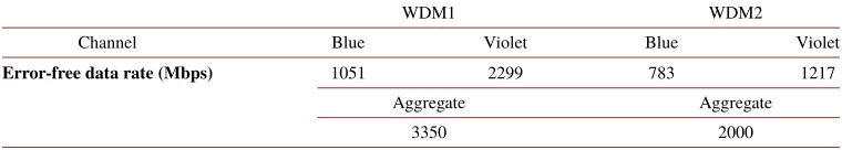
[image:9.612.116.497.258.325.2]Error-free data rates, calculated by applying the 7% FEC overhead reduction, for blue and green micro-LEDs and their aggregate in each WDM set-up are shown in Table1. In aggregate, 1.79 and 1.54 Gbps error-free date rates are achieved in the WDM1 and WDM2 set-ups, respectively.
Table 1. Error-free data rates for each channel and aggregated in WDM1 and WDM2 set-ups achieved by the blue-green micro-LEDs array.
WDM1 WDM2
Channel Blue Green Blue Green
Error-free data rate (Mbps) 1173 620 1158 381
Aggregate Aggregate
1793 1539
3.5. Communication performance of the blue-violet micro-LED array
The blue-violet micro-LED array operation as a WDM transmitter followed the same approach as the blue-green one. In this case, the blue and violet micro-LEDs were operated at the same current density as the blue and green micro-LEDs, respectively. The SNR and number of allocated bits, at the highest rate below FEC threshold, in both WDM set-ups for the blue and violet micro-LEDs are shown in Figs.6(a) and6(b), respectively.
The blue and violet micro-LED channels maximum SNR is quite similar due their comparable optical power. Nonetheless, due to the violet micro-LED higher -6 dB electrical modulation bandwidth, the violet channel supports bit allocation up until 650 MHz. The introduction of the dichroic mirror, which has cut-off wavelength at 425 nm, results in a loss of optical power and, thus lower SNR for both channels, limiting the maximum achievable data rate in WDM2. The violet (reflected) channel is more affected than the blue one due to the optical response of the dichroic mirror, with estimated optical power losses of 11%. The BERvsdata transmission curve is presented in Fig.6(c). The maximum data rates, below FEC threshold, achieved by the blue and violet micro-LEDs in the WDM1 set-up are 1130 and 2472 Mbps, respectively. In the WDM2 set-up the maximum data rates, below FEC threshold, achieved by the blue and violet micro-LEDs drop to 842 and 1309 Mbps, respectively.
The blue and violet channels and aggregate error-free data rates for WDM1 and WDM2 set-ups are shown in Table2. In aggregate, the blue-green micro-LED array achieves error-free data rates of 3.35 and 2 Gbps, in the WDM1 and WDM2 set-ups, respectively.
Table 2. Error-free data rates for each channel and aggregated in WDM1 and WDM2 set-ups achieved by the blue-violet micro-LED array.
WDM1 WDM2
Channel Blue Violet Blue Violet
Error-free data rate (Mbps) 1051 2299 783 1217
Aggregate Aggregate
[image:9.612.116.496.622.690.2]Fig. 6.Signal-to-noise ratio and allocated bits (at maximum data rate below forward error correction) in both WDM set-ups achieved by (a) the blue micro-LED and (b) the violet micro-LED; (c) BERvsdata rate for blue and violet micro-LEDs in both WDM set-ups.
4. Conclusions
In conclusion, we have demonstrated the fabrication, characterization and VLC application of on-chip dual-color micro-LED arrays. Blue-green and blue-violet micro-LED arrays were fabricated by transfer printing a blue emitting micro-LED onto the substrate of the green and violet micro-LEDs, respectively. The violet, green, and blue individual micro-LEDs exhibit an optical power of 0.85, 0.34, and 1.04 mW, at the current densities of 2.8 kA/cm2, 2.8 kA/cm2, and 138 A/cm2, respectively. The violet, green, and blue present -6 dB electrical modulation bandwidths up to 427, 144, and 134 MHz, respectively. Operation of the blue-green micro-LED array at different biases allows one to fine tune the perceived color from blue (x0.15;y0.04) to green (x0.11;y0.71) on the CIE1931 color diagram. Due to the human eye’s poorer optical response in the blue-violet spectral region, operation of the blue-violet micro-LED array at different biases results in a very small variation of its color coordinates. In the two free space WDM VLC set-ups investigated in this work, the blue-green micro-LED array achieves an aggregated error-free data rate of 1.79 and 1.54 Gbps and the blue-violet micro-LED array 3.35 and 2 Gbps.
The two on-chip dual-color micro-LED arrays reported in this work can potentially be integrated into the same package to give a 3-color output. Furthermore, these on-chip dual color micro-LED arrays should be suitable for underwater and plastic optical fiber VLC, as the micro-LED EL spectra match both mediums transparency windows. This work opens the way to multi-colored pixelated clusters in micro-LED displays acting as WDM visible light communications links.
Funding
Engineering and Physical Sciences Research Council (EP/L015595/1, EP/M01326X/1).
Acknowledgments
The authors would like to thank P. Hill and J. Smith for the atomic force microscopy measurements. Plessey Semiconductors is acknowledged for providing the GaN-on-Si material.
References
1. H. X. Jiang and J. Y. Lin, “Nitride micro-LEDs and beyond - a decade progress review,”Opt. Express21(S3), A475 (2013).
2. J. Herrnsdorf, J. J. D. McKendry, S. Zhang, E. Xie, R. Ferreira, D. Massoubre, A. M. Zuhdi, R. K. Henderson, I. Underwood, S. Watson, A. E. Kelly, E. Gu, and M. D. Dawson, “Active-Matrix GaN Micro Light-Emitting Diode Display With Unprecedented Brightness,”IEEE Trans. Electron Devices62(6), 1918–1925 (2015).
3. S. Zhang, Z. Gong, J. J. D. McKendry, S. Watson, A. Cogman, E. Xie, P. Tian, E. Gu, Z. Chen, G. Zhang, A. E. Kelly, R. K. Henderson, and M. D. Dawson, “CMOS-Controlled Color-Tunable Smart Display,”IEEE Photonics J.
4(5), 1639–1646 (2012).
4. F. Templier, “GaN-based emissive microdisplays: A very promising technology for compact, ultra-high brightness display systems,”J. Soc. Inf. Disp.24(11), 669–675 (2016).
5. S. Rajbhandari, J. J. D. McKendry, J. Herrnsdorf, H. Chun, G. Faulkner, H. Haas, I. M. Watson, D. O’Brien, and M. D. Dawson, “A review of gallium nitride LEDs for multi-gigabit-per-second visible light data communications,” Semicond. Sci. Technol.32(2), 023001 (2017).
6. X. Li, L. Wu, Z. Liu, B. Hussain, W. C. Chong, K. M. Lau, and C. P. Yue, “Design and Characterization of Active Matrix LED Microdisplays With Embedded Visible Light Communication Transmitter,”J. Lightwave Technol.
34(14), 3449–3457 (2016).
7. Y. Wang, B. R. Rae, R. K. Henderson, Z. Gong, J. Mckendry, E. Gu, M. D. Dawson, G. A. Turnbull, and I. D. W. Samuel, “Ultra-portable explosives sensor based on a CMOS fluorescence lifetime analysis micro-system,”AIP Adv.
1(3), 032115 (2011).
8. A. Zarowna-Dabrowska, S. L. Neale, D. Massoubre, J. McKendry, B. R. Rae, R. K. Henderson, M. J. Rose, H. Yin, J. M. Cooper, E. Gu, and M. D. Dawson, “Miniaturized optoelectronic tweezers controlled by GaN micro-pixel light emitting diode arrays,”Opt. Express19(3), 2720 (2011).
9. K. Chung, J. Sui, B. Demory, C.-H. Teng, and P.-C. Ku, “Monolithic integration of individually addressable light-emitting diode color pixels,”Appl. Phys. Lett.110(11), 111103 (2017).
10. Y.-H. Ra, R. Wang, S. Y. Woo, M. Djavid, S. M. Sadaf, J. Lee, G. A. Botton, and Z. Mi, “Full-Color Single Nanowire Pixels for Projection Displays,”Nano Lett.16(7), 4608–4615 (2016).
11. Y. J. Hong, C.-H. Lee, A. Yoon, M. Kim, H.-K. Seong, H. J. Chung, C. Sone, Y. J. Park, and G.-C. Yi, “Visible-Color-Tunable Light-Emitting Diodes,”Adv. Mater.23(29), 3284–3288 (2011).
12. C.-M. Kang, J.-Y. Lee, D.-J. Kong, J.-P. Shim, S. Kim, S.-H. Mun, S.-Y. Choi, M.-D. Park, J. Kim, and D.-S. Lee, “Hybrid Full-Color Inorganic Light-Emitting Diodes Integrated on a Single Wafer Using Selective Area Growth and Adhesive Bonding,”ACS Photonics5(11), 4413–4422 (2018).
13. H. Zhang and J. A. Rogers, “Recent Advances in Flexible Inorganic Light Emitting Diodes: From Materials Design to Integrated Optoelectronic Platforms,”Adv. Opt. Mater.7(2), 1800936 (2019).
14. H. Kim, E. Brueckner, J. Song, Y. Li, S. Kim, C. Lu, J. Sulkin, K. Choquette, Y. Huang, R. G. Nuzzo, and J. A. Rogers, “Unusual strategies for using indium gallium nitride grown on silicon (111) for solid-state lighting,”Proc. Natl. Acad. Sci. U. S. A.108(25), 10072–10077 (2011).
15. M. Choi, B. Jang, W. Lee, S. Lee, T. W. Kim, H.-J. Lee, J.-H. Kim, and J.-H. Ahn, “Stretchable Active Matrix Inorganic Light-Emitting Diode Display Enabled by Overlay-Aligned Roll-Transfer Printing,”Adv. Funct. Mater.
27(11), 1606005 (2017).
16. M. K. Choi, J. Yang, K. Kang, D. C. Kim, C. Choi, C. Park, S. J. Kim, S. I. Chae, T.-H. Kim, J. H. Kim, T. Hyeon, and D.-H. Kim, “Wearable red–green–blue quantum dot light-emitting diode array using high-resolution intaglio transfer printing,”Nat. Commun.6(1), 7149 (2015).
17. C. A. Bower, M. A. Meitl, B. Raymond, E. Radauscher, R. Cok, S. Bonafede, D. Gomez, T. Moore, C. Prevatte, B. Fisher, R. Rotzoll, G. A. Melnik, A. Fecioru, and A. J. Trindade, “Emissive displays with transfer-printed assemblies of 8 µm×15 µm inorganic light-emitting diodes,”Photonics Res.5(2), A23 (2017).
18. D. Tsonev, H. Chun, S. Rajbhandari, J. J. D. McKendry, S. Videv, E. Gu, M. Haji, S. Watson, A. E. Kelly, G. Faulkner, M. D. Dawson, H. Haas, and D. O’Brien, “A 3-Gb/s Single-LED OFDM-Based Wireless VLC Link Using a Gallium Nitride µLED,”IEEE Photonics Technol. Lett.26(7), 637–640 (2014).
20. M. S. Islim, R. X. Ferreira, X. He, E. Xie, S. Videv, S. Viola, S. Watson, N. Bamiedakis, R. V. Penty, I. H. White, A. E. Kelly, E. Gu, H. Haas, and M. D. Dawson, “Towards 10 Gb/s orthogonal frequency division multiplexing-based visible light communication using a GaN violet micro-LED,”Photonics Res.5(2), A35 (2017).
21. H. Chun, S. Rajbhandari, G. Faulkner, D. Tsonev, E. Xie, J. J. D. McKendry, E. Gu, M. D. Dawson, D. C. O’Brien, and H. Haas, “LED Based Wavelength Division Multiplexed 10 Gb/s Visible Light Communications,”J. Lightwave Technol.34(13), 3047–3052 (2016).
22. A. J. Trindade, B. Guilhabert, D. Massoubre, D. Zhu, N. Laurand, E. Gu, I. M. Watson, C. J. Humphreys, and M. D. Dawson, “Nanoscale-accuracy transfer printing of ultra-thin AlInGaN light-emitting diodes onto mechanically flexible substrates,”Appl. Phys. Lett.103(25), 253302 (2013).
23. A. J. Trindade, B. Guilhabert, E. Y. Xie, R. Ferreira, J. J. D. McKendry, D. Zhu, N. Laurand, E. Gu, D. J. Wallis, I. M. Watson, C. J. Humphreys, and M. D. Dawson, “Heterogeneous integration of gallium nitride light-emitting diodes on diamond and silica by transfer printing,”Opt. Express23(7), 9329 (2015).
24. D. Kang, A. Standley, J. H.-C. Chang, Y. Liu, and Y.-C. Tai, “Effects of deposition temperature on Parylene-C properties,” in2013 IEEE 26th International Conference on Micro Electro Mechanical Systems (MEMS)(IEEE, 2013), pp. 389–390.
25. H. M. Ng, N. G. Weimann, and A. Chowdhury, “GaN nanotip pyramids formed by anisotropic etching,”J. Appl. Phys.94(1), 650–653 (2003).
26. J.-H. Ryou, P. D. Yoder, J. Liu, Z. Lochner, H. Kim, S. Choi, H. J. Kim, and R. D. Dupuis, “Control of Quantum-Confined Stark Effect in InGaN-Based Quantum Wells,”IEEE J. Sel. Top. Quantum Electron.15(4), 1080–1091 (2009).