Abstract: Multi-phase Induction motor drives (MPIMD) with numerous advantages dominates three-phase drives and emerges as a potential contender and viable solution for the high power electric drive applications. When multi-phase AC drives fed from voltage source inverters (VSIs) requires a suitable PWM method of control. This paper investigates the performance of 5-ϕ induction motor drive with various space vector PWM (SVPWM) techniques. First, a 5-ϕ VSI model is presented in terms of space vectors. Next, modified SVPWM switching techniques are introduced based on medium, large and the combination of medium and large vectors, which provide its working with reduced %THD in the output voltages. The proposed scheme uses the full DC bus voltage, and the output response superior with low lower order harmonics than the conventional SVPWM methods. The performances of the 5-ϕ VSI fed IM drive tested with various switching techniques, and the results observed in terms of harmonic contents present in the output voltage waveform. MATLAB/Simulink software results included in this paper to show and verify the theoretical concepts.
Index Terms: SVPWM, five-phase VSI, five-phase induction motor, total harmonic distortion
I. INTRODUCTION
In general, multi-phase systems have many advantages, and they are used in applications such as automotive industry, aeronautics and electric power generation due to a variety of benefits provided by multi-phase drives over 3-ϕ drives. [1]. In the case of even number phases, the poles are coinciding with each other, and it will reduce the motor performance. So, odd number phases are preferred over even number phases [2]-[3]. Also, the output power of a 5-ϕ system is greater than that of the 3-ϕ system. This has attracted the interest in the development of multi phase machines [4], [5].
The broad choice of switching techniques can be used for the VSI to produce the expected output [6]-[9]. The techniques start with sin triangle PWM, conventional SVPWM, and modified SVPWM. SVPWM technique is more suitable for multiphase VSI, and the no. of vectors increase with the no. of a levels and no. of phases (i.e., 'm' is the no. of level of VSI and 'n' is the no. of phases) [10], [11]. A 2 level VSI has 32 vectors represented into d1-q1 & d3-q3 subspaces. All subspaces are a source of lower order harmonics except the d1-q1 subspace. The switching techniques proposed in [12] can eliminate the harmonics
Revised Manuscript Received on May 10 ,2019
D. Raja, Research Scholar, Department of EEE, Pondicherry
Engineering College, Pillaichavady, Puducherry, India,
G. Ravi, Professor, Department of EEE, Pondicherry Engineering College, Pillaichavady, Puducherry, India.
present in d3-q3. In addition, this method can generate a sinusoidal phase voltage waveform. There are few SVPWM techniques proposed in [13]-[16] to minimize the switching losses of a 5-ϕ inverter.
The SVPWM with modified switching scheme is proposed in this paper for the 5-ϕ VSI fed IM drive. The MATLAB/ Simulink is used to construct the system. The performances of the proposed techniques are compared with conventional SVPWM technique.
II. MODELINGOFFIVEPHASEINDUCTION MOTOR
A Mathematical model can be represented for an induction motor. The 5-ϕ system variables are transformed into 2-ϕ variables in d-q plane rotating with synchronous speed. The displacement between two phases is 72 degrees, and the number of phases must be the same before and after the transformation. The relationships between 5-ϕ and 2-ϕ variables are as follows.
Vdq =s KS Vabcdes idq =s KS iabcdes Ѱdq =s KS Ѱabcdes (1)
Vdq =r Kr Vabcder idq =r Kr iabcder Ѱdq =r Kr Ѱabcder (2) Where,
K = 25
1 cos 25π cos 4π
5 cos 4π
5 cos 2π
5
0 sin 25π sin 45π sin 45π sin(25π) 1 cos 45π cos 85π cos 85π cos 45π
0 sin 45π sin 85π − sin 85π −sin 45π
1
2 1 2
1 2
1 2
1 2
(3)
„K‟ is the 5-ϕ induction machine decoupling transformation matrix given in equation 2. The 5-ϕ machine is represented in the d-q-x-y-o arbitrary plane. The d-q components are responsible for power generation, fluxes and torque production in the machine. System losses are accounted by x-y components, and the reason for zero components being used is to show unchanged in the system. The 5-ϕ IM is modeled in the MATLAB Simulink, and the characteristics responses are obtained.
Essential machine model equations for stator sides and rotor sides in stationary reference frame are represented as follows:
Vds = Rsids + pѰds
Vqs = Rsiqs + pѰqs (4)
Ѱxs = Llsixs
Analysis of Five Phase Inverter with different
SVPWM Switching Techniques for Induction
Motor Drive
Ѱys = Llsiys (5)
Vdr = Rridr+ pѰdr Vqr = Rriqr+ pѰqr (6) Ѱxr = Llrixr Ѱyr= Llriyr (7) Flux Linkage equations for stator and rotor sides are expressed as follows:
Ѱxs = Llsixs Ѱxr = Llrixr (8) Ѱds = Lls + Lm ids + Lmidr
Ѱqs = Lls + Lm iqs + Lmiqr (9) Ѱdr = Llr+ Lm idr + Lmids
Ѱqr = Llr+ Lm iqr + Lmiqs (10)
Where, Ls= Lls+ Lm Lr = Llr+ Lm (11) Ѱys = Llsiys Ѱyr = Llriyr (12)
The equation for torque can be denoted as:
Te= PLm(idriqs − idsidr) (13) ѡr= P
2J(Te− TL) (14)
III. TWO-LEVELFIVE-PHASEVSI
Multi-phase IM drives used for variable speed applications. The conventional multiphase VSI does not suitable for this application owing to the high amount of harmonics presented in the voltage waveforms. A space vector concept is used with a modified switching sequence to reduce the harmonics and also helps to maximize the fundamental voltage.
Fig.1 shows the circuit diagram for 5-ϕ VSI fed 5-ϕ IM drive comprises ten power switches, two switches per leg. The pole voltage is equal to Vdc when the upper switch is ON and it is zero when it is OFF. To avoid the direct short circuit of same leg switches, they switched opposite to each other.
Phase to neutral voltages (Va ~ Ve) of 5-ϕ VSI can be expressed in terms of inverter pole voltages as given in equation (15) and (16) [12].
Vj=45Vj−15 5i,i≠jVj, if j < 5 (15)
Vj=45Vj−15 4i,i≠jVj, if j = 5 (16)
In general, a 5-ϕ 2-level VSI has 32 combinations of switching states (ie., 2n, where n is the number of phases) and can be represented in two space vector planes (d1-q1 and d3-q3) includes thirty active and two zero vectors.
[image:2.595.45.302.49.255.2]Binary numbers are used to represent the states on each space vectors. Bit „0‟ represents that the lower switch is ON while a bit „1‟ represents that the upper switch is on. The three coordinated decagons formed by 30 active vectors originate at the 2 zero vectors. Inner, middle and outer decagons magnitudes are 0.2472, 0.4, and 0.6472.
Fig 2 and Fig. 3 shows the space vector representation in a d-q plane. The phase sequence in d1q1 is ABCDE while in d3q3 it is ACEBD. The middle decagon is the same in both subspaces while the inner and outer decagons are interchanged between d1q1 and d3q3.equation (17) and (18) represents the 5-ϕ inverter voltage in a two-phase d-q plane. The value of a, a2, a3, & a4 is given in equation (19) to (22).
Vd1q1=25Vdc[Va+ aVb+ a2Vc+ a3Vd+ a4Ve] (17)
Vd3q3=25Vdc[Va+ aVc+ a2Ve+ a3Vb+ a4Vd] (18)
Where,
a = cos25π+ sin25π (19)
a2= cos4π 5 + sin
4π
5 (20)
a3= cos4π 5 − sin
4π
5 (21)
a4= cos2π 5 − sin
2π
5 (22)
Fig. 15-ϕ VSI fed 5-ϕ IM drive
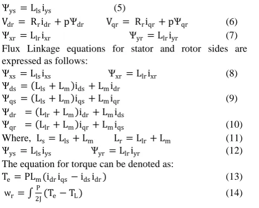
IV. SVPWMSWITCHINGSCHEMESFOR5-ΦVSI A. Switching Scheme I: Using Medium Vectors in
(d1q1 plane)
The medium decagon of a d1q1 plane is considered in this
elementary space vector (SV) modulation switching scheme for 5-ϕ VSI. The switching vector rotates in an anti-clockwise direction starting from V16 until V30 is reached as shown in
Fig. 2. The equations (23), (24) & (25) used to calculate the conduction time in each switching state. Fig. 4 (a) & (b) shows the upper IGBT conventional and modified switching pattern in each phase and the respective switching vector shown in Fig. 5 (a). In conventional switching scheme, the switching vectors start from 0, 16, 29, 31, 31, 29, 16, and 0 for one switching cycle Ts in sector I. while the zero
switching vector 31 is eliminated in modified switching scheme. Fig. 5(b) & (C) shows the modulating signals for conventional and modified switching schemes.
The conduction time of each switching state is calculated by using the following expressions.
tam =
Vref sin K5π −θ
Vmsin 5π ts (23)
tbm =
Vref sin θ− K−1 π5
Vmsin π5 ts (24)
[image:2.595.301.545.56.315.2]Vmax = Vm cos10π Vdc = 0.3804Vdc (26)
Fig. 2Switching vectors in d1-q1 Subspace
Fig. 3Switching vectors in d3-q3 Subspace
(a)
(b)
Fig. 4switching pattern for Medium vectors in d1-q1
Subspace in Sector -I (a) conventional (b) Modified
(a)
(b)
(c)
Fig.5 (a) Time Switching for Medium vectors in d1-q1
Subspace in Sector -I (b) conventional & (c) Modified Modulating signal
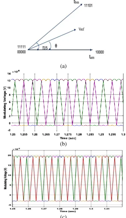
B. Switching Scheme II: Using Large Vectors (d1q1 plane)
The Space Vectors in the large decagon of d1q1 plane
[image:3.595.319.522.52.206.2] [image:3.595.321.541.267.647.2] [image:3.595.78.290.287.459.2] [image:3.595.62.270.502.657.2]switching vector rotates in an anti-clockwise direction starting from V25 until V17 as shown in Fig. 2. The equations
(27), (28) & (29) used to calculate the conduction time in each switching state. Fig. 6 (a) & (b) shows the upper IGBT switching pattern in each phase and the respective switching vector has shown in Fig. 7 (a). In conventional switching scheme, the switching vectors start from 0, 25, 24, 31, 31, 24, 25, and 0 for one switching cycle Ts in sector I. while the zero
switching vector 31 is eliminated in modified switching scheme. Fig. 7 (b) & (C) shows the modulating signals for conventional and modified switching schemes.
The following expressions are used to calculate the conduction time tal, tbl and to.
tal =
Vref sin Kπ5 −θ
Vlsin π5 ts (27)
tbl =
Vref sin θ− K−1 π5
Vlsin π5 ts (28)
t0=ts−tal2−tbl (29)
Maximum possible fundamental peak voltage of large space vector is
Vmax = Vl cos10π Vdc = 0.6155Vdc (30)
(a)
(b)
Fig. 6switching pattern for large vectors in d1-q1 Subspace in
Sector -I (a) conventional (b) Modified
(a)
(b)
[image:4.595.321.534.59.499.2](c)
Fig.7 Time Switching for Large vectors in d1-q1 subspace in
Sector –I (b) conventional & (c) Modified Modulating signal
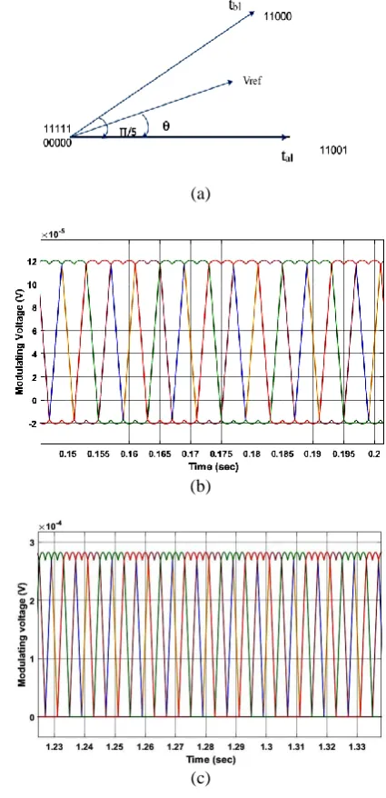
C. Switching Scheme III: Using combination of medium and Large Vectors (d1q1 plane)
Instead of using only two active and two zero vectors, four active and two zero vectors can be used for the five phase VSI. Fig. 8 (a) & (b) shows the upper IGBT switching pattern in each phase and the respective switching vector has shown in Fig. 9 (a). In conventional switching scheme, the
switching vectors start from 0, 16, 24,
25,29,31,31,29,25,24,16,0 for one switching cycle Ts in
sector I. while the zero switching vectors 31 is eliminated in modified switching scheme. Fig. 9 (b) & (C) shows the modulating signals for conventional and modified switching schemes.
The following expressions are used to calculate the conduction time tam, tbm, tal, tbl and to.
[image:4.595.58.289.356.717.2]tb= tbl+ tbm (32)
The Maximum possible fundamental peak voltage of combinations of medium and large space vector is
Vm cos10π Vdc ≤ Vmax ≤ Vl cos10π Vdc (33)
(a)
(b)
Fig. 8switching pattern for combination of medium and Large Vectorsin d1-q1 Subspace in Sector -I (a) conventional
(b) Modified
(a)
(b)
(c)
Fig.9Time switching for combination of medium and Large Vectorsin d1-q1 Subspace in Sector –I (b) conventional & (c)
Modified modulating signal
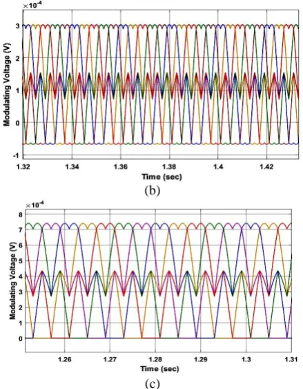
V. SIMULATIONRESULTS
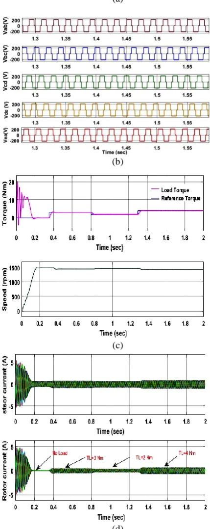
[image:5.595.321.541.51.333.2] [image:5.595.63.279.107.506.2] [image:5.595.93.264.572.712.2](a)
(b)
(c)
[image:6.595.303.552.79.231.2](d)
Fig. 10 Performance characteristics of 5-ϕ SVPWM VSI fed IM Drive (a) Phase Voltage (b) Line Voltage (c) Speed &
torque response (d) stator & rotor current
Table 1
Parameters of 5-ϕ VSI fed IM Drive
Parameters Values
DC Bus voltage 400 V
Switching frequency 5 KHz
Motor RMS Input Voltage (V) 220
No. of Phases 5
Number of Poles (p) 4
Resistance (stator) 10.1 Ω
Inductance (stator) 0.833 Henry
Resistance (rotor) 9.854 Ω
Inductance (rotor) 0.782 Henry
Mutual Inductance 0.782 Henry
Inertia 0.0088
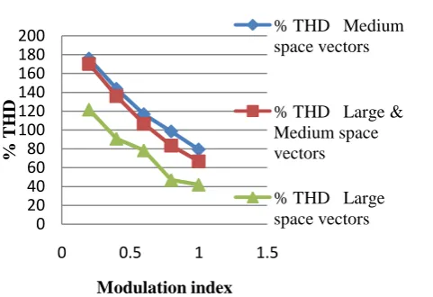
Two different SVPWM switching schemes are designed for 5-ϕ SVPWM VSI fed IM drive. The output phase fundamental voltage and total harmonic distortions are considered as the factors to identify the best switching scheme for 5-ϕ VSI. Also, these two factors are obtained for different values of the modulation index. The fundamental voltage peak is high for the modified SVPWM switching scheme when compared to conventional SVPWM technique as noted from Fig. 11 and Fig.13. The %THD in the phase voltage of 5-ϕ SVPWM VSI fed IM drive is observed for different modulation index is as shown in the Fig.12 and Fig.14.
From the comparative results of SVPWM switching techniques, the d1-q1 large vector switching produces the %
[image:6.595.48.263.205.745.2]THD of 30.09% whereas the conventional SVPWM its value is about 42.14%. Therefore it is inferred that the 5-ϕ VSI with large vector SVPWM switching scheme gives the optimum results for the output voltage fundamental peak and lower % voltage THD.
Fig. 11 Fundamental voltage peak (p.u) for different conventional SVPWM switching schemes 0
0.1 0.2 0.3 0.4 0.5 0.6 0.7
0 1 2
F
un
da
m
ent
a
l
v
o
lt
a
g
e
pea
k
(
p.u)
Modulation index
Fundamental Voltage Peak (pu) Medium space vectors
Fundamental Voltage Peak (pu) Large & Medium space vectors
[image:6.595.317.546.504.651.2]Fig. 12 % THD in phase voltage for different conventional SVPWM switching schemes
Fig. 13 Fundamental voltage peak (p.u) for different modified SVPWM switching schemes
Fig. 14 % THD in phase voltage for different modified SVPWM switching schemes
VI. CONCLUSION
A 5- ϕ VSI with various SVPWM techniques are presented to improve the power quality of input voltage applied to 5-ϕ IM drive. Use of SVPWM techniques improves the utilization of DC bus voltage when compared to SPWM techniques. This control technique also improves the
fundamental output voltage by 25% greater than the sinusoidal pulse width modulation techniques. This investigation is performed in the MATLAB Simulink for 5-ϕ VSI fed IM drive. The results of fundamental voltage and % THD in the output voltage for different switching schemes in d1q1 subspaces are obtained. These comparison result shows
that d1-q1 large vector switching technique gives the
maximum fundamental voltage and lesser %THD in output voltage than other methods.
REFERENCES
1. Subodh Kanta Barika, Kiran Kumar Jaladi “Five-Phase IM DTC-SVM sche. with PI Control. & ANN control.” Publi. by Elsevier Ltd in Procedia Tech. 25 (2016) 816 – 823.
2. K. B. Yadav, Alok Kumar Mohanty, Prabhat Kumar, “Recent Research Trend on Multi-phase Induction Machines” Proc. of Int. Conf. on Control, Communi. and Power Engg., CCPE, Elsevier- 2014. pp. 580 -586.
3. K.S. kumar, Das. A, Ramchand. R, Patel.C & K. G.kumar, “A 5-level inv. scheme for a 4-pole IM drive by feeding the identical voltage-profile windgs from both sides,” IEEE Tra. Indu. Electr., vol. 57, no. 8, pp. 2776–2784, Aug. 2010.
4. A. S. A Khalik, S. Ahmed, A. A. E, & A. Massoud, “Effect of stator wdg connection of 5-ϕ IM on Torque Ripples Under Open Line Condition”, IEEE Tran.. Mechatronic, vol. 20, no. 2, pp. 580–593, April. 2015.
5. Levi, E, Bojoi, R, Profumo, F, Toliyat, HA and Williamson, S (2007) Multiphase induction motor drives - a technology status review IET electric power applications, 1 (4). pp. 489-516.
6. E.Levi “ Multi ϕ IM drive – a technolo. tatus review” IET Elec.. Pow. App. Vol. 1, No.4, pp.489-516, July 2007.
7. E. Levi, "Multiphase Electric Machines for Variable-Speed Applications," in IEEE Transactions on Industrial Electronics, vol. 55,
no. 5, pp. 1893-1909, May 2008.
doi: 10.1109/TIE.2008.918488
8. MK K Sahu, AK K Panda, BP Panigrahi “DTC for 3-Level NPC Inverter-Fed IM Drive” ETASR – Engg., Tech. & Applied Science Res. Vol. 2, No. 2, 2012, 201-208.
9. B. Jyothi and Dr.M.Venu Gopala Rao“Comparison of Five Leg Inv. and Five Phase Full Bridge Inv. for Five Ph. Supply”, Int. Conf. on ISEG 19-20 Sept. 2014.
10. A. Iqbal, S. Moinuddin and M. R. Khan, "Space Vector Model of A Five-Phase Voltage Source Inverter," 2006 IEEE International Conference on Industrial Technology, Mumbai, 2006, pp. 488-493. 11. S. Moinoddin and A. Iqbal, "Space vector model of a five-phase current
source inverter," 2016 Biennial International Conference on Power and Energy Systems: Towards Sustainable Energy (PESTSE), Bangalore, 2016, pp. 1-6.
12. Wan Noraishah Wan Abdul Munim, Mohd Firdaus Ismail, Ahmad Farid Abidin, and Harizan Che Mat Haris, “Multi-phase Inverter Space Vector Modulation”, IEEE 7th International power engineering and optimization conference ,3-4 june 2013, pp.149-154.
13. Mahmoud Gaballah, Mohammed El-Bardini, “Low cost digital signal generation for driving space vector PWM inverter”, Ain Shams Engineering Journal, Volume 4, Issue 4, 2013, Pages 763-774, ISSN 2090-4479.
14. Nanda Kumar, S., Vijayan, S. & Nanda Kumar, E.” Asymmetric SVM Technique for Minimizing Switching Loss of Inverter” Arabian Journal for Science and Engineering (2014) 39: 3123.
15. Devisree Sasi , Jisha Kuruvilla P , Anish Gopinath, “Generalized SVPWM Algorithm for Two Legged Three Phase Multilevel Inverter”, International Journal of Power Electronics and Drive System (IJPEDS) Vol.3, No.3, September 2013, pp. 279-286 ISSN: 2088-8694. 16. P. Sala-Perez, S. Galceran-Arellano, D. Montesinos-Miracle. "A
sensorless stable V/f control method for a five-phase PMSM" , 2013 15th European Conference on Power Electronics and Applications (EPE), 2013. 0 20 40 60 80 100 120 140 160 180 200
0 0.5 1 1.5
%
T
H
D
Modulation index
% THD Medium space vectors
% THD Large & Medium space vectors
% THD Large space vectors 0 0.1 0.2 0.3 0.4 0.5 0.6 0.7
0 1 2
F un da m ent a l v o lt a g e pea k (p .u) Modulation index Fundamental Voltage Peak (pu) Medium space vectors
Fundamental Voltage Peak (pu) Large & Medium space vectors
Fundamental Voltage Peak (pu) Large space vectors 0 20 40 60 80 100 120 140 160 180
0 1 2
%
T
H
D
Modulation index
% THD Medium space vectors
% THD Large & Medium space vectors