www.advopticalmat.de
Optical Detection and Spatial Modulation of Mid-Infrared
Surface Plasmon Polaritons in a Highly
Doped Semiconductor
Davide Maria Di Paola,* Anton V. Velichko, Mario Bomers, Nilanthy Balakrishnan,
Oleg Makarovsky, Mario Capizzi, Laurent Cerutti, Alexei N. Baranov, Manoj Kesaria,
Anthony Krier, Thierry Taliercio, and Amalia Patanè*
DOI: 10.1002/adom.201700492
scattering in thin films, surface rough-ness, etc.; chemical instability in air and low compatibility with silicon tech-nology represent further limitations to the exploitation of metals;[1] also, given their high carrier densities (1022–1023 cm−3), metals usually have plasma frequencies,
ωp, in the visible–UV spectral ranges. On the other hand, highly doped semiconduc-tors (HDSCs) present several appealing features:[2,3] first, the lower carrier densities (1016–1020 cm−3) enable plasma frequencies in the mid-infrared (MIR) spectral range, of relevance for technologically important applications, including gas detection and biosensing;[4,5] second, the carrier density and the plasmonic resonance can be tuned either by doping or geometrical patterning of semiconductors,[6] thus enabling routes to cost-effective and compact all-semicon-ductor plasmonic structures.[7,8]
Achieving a high doping in a semiconductor can be lim-ited by the solid solubility of the dopants[9,10] and/or by doping compensation effects.[11,12] In addition, a high density of dopants can degrade the crystal quality and induce internal losses. Thus, finding low-loss semiconductor materials for plasmonics presents challenges of fundamental and techno-logical interest.[13] To date, a number of HDSCs have been successfully tested, including transparent conducting oxides, such as aluminum and gallium zinc oxide,[14] indium tin oxide,[15] and dysprosium cadmium oxide.[16] These materials have plasmonic resonances in the near-infrared[14,15] and MIR spectral range.[16] Compounds such as SiC,[17] (InGa)As,[18] and In(AsSb)[6,8,19] have also shown good response in the MIR.[20] The III–V semiconductor InAs features as a relatively recent addition to this group: it can sustain high doping concen-trations[10,21] with plasmonic resonances over a broad MIR range.[22] Furthermore, the incorporation of small quantities of nitrogen (N < 3%) into the group-V sublattice of InAs to form the dilute nitride alloy In(AsN) enables the engineering of fun-damental band properties and the behavior of dopants.[23,24] For example, the incorporation of nitrogen in InAs reduces the band gap energy of the material, while that of hydrogen in In(AsN) increases the electron density by two orders of mag-nitude, up to 1019 cm−3.[25] This enhancement, not observed in InAs or reported for other dilute nitride alloys, is due to the N-atoms, which act as H traps to form NH donor complexes Highly doped semiconductors (HDSCs) are promising candidates for
plas-monic applications in the mid-infrared (MIR) spectral range. This work exam-ines a recent addition to the HDSC family, the dilute nitride alloy In(AsN). Postgrowth hydrogenation of In(AsN) creates a highly conducting channel near the surface and a surface plasmon polariton detected by attenuated total reflection techniques. The suppression of plasmonic effects following a photoannealing of the semiconductor is attributed to the dissociation of the NH bond. This offers new routes for direct patterning of MIR plasmonic structures by laser writing.
D. M. Di Paola, Dr. A. V. Velichko, Dr. N. Balakrishnan, Dr. O. Makarovsky, Prof. A. Patanè
School of Physics and Astronomy The University of Nottingham Nottingham NG7 2RD, UK
E-mail: [email protected]; [email protected] M. Bomers, Dr. L. Cerutti, Dr. A. N. Baranov, Prof. T. Taliercio
IES l’institut d’électronique
Univ. Montpellier and CNRS UMR 5214 F-34000 Montpellier, France
Prof. M. Capizzi Dipartimento di Fisica Sapienza Università di Roma Piazzale A. Moro 2, 00185 Roma, Italy Dr. M. Kesaria, Prof. A. Krier Physics Department Lancaster University Lancaster LA1 4YB, UK
The ORCID identification number(s) for the author(s) of this article can be found under https://doi.org/10.1002/adom.201700492. Surface Plasmon Polaritons
1. Introduction
Plasmonics generally relies on metals due to the high den-sity of free electrons. However, metals also suffer from sub-stantial losses due to interband transitions, grain-boundary
within a thin (≈0.1–1 µm) channel below the surface.[26] Secondary ion mass spec-troscopy has shown that the H-distribution has a box-shaped form, from which the H-penetration depth can be estimated.[26,27] Also, the NH complexes are stable under normal conditions and do not degrade with time.[27] In stark contrast to what observed in other dilute nitride alloys, such as Ga(AsN), Ga(PN), and (InGa)(AsN),[28,29] the H-dopants in In(AsN) do not neutralize the electronic activity of the N-atoms. Thus, the band gap energy of In(AsN) does not change upon H-incorporation.[27]
Here, we demonstrate that the H-enhanced conductivity near the surface of In(AsN) cre-ates a surface plasmon polariton (SPP) mode confined at the air–semiconductor interface, which we detect via attenuated total reflection (ATR) measurements. The modulation of the carrier density by removal of H is demon-strated by laser annealing and Raman spec-troscopy: the phonon–plasmon coupled mode induced by H can be suppressed locally by a thermal annealing with a focused laser beam. These findings demonstrate a new approach to MIR-plasmonics via postgrowth H-implan-tation and laser writing of In(AsN).
2. Results and Discussion
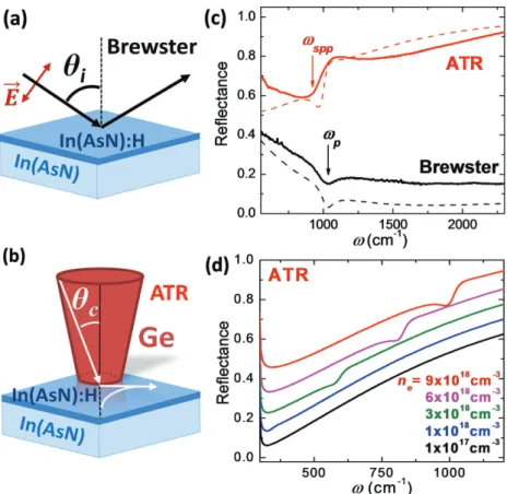
2.1. Reflectance Spectroscopy of Surface Plasmon PolaritonsFor these studies, we used hydrogenated In(AsN) epilayers with thickness t = 0.3 µm (1 µm) and N-content x = 1% (1.1%)
grown by molecular-beam-epitaxy (MBE) on a GaAs sub-strate. We also examined control samples based on Si-doped InAs epilayers grown by MBE on an InAs substrate (t = 1.3, 2.1, and 2.7 µm). The reflectance spectra on the In(AsN):H epilayers were acquired in the Brewster (Figure 1a) and the ATR (Figure 1b) configuration. Figure 1c shows the reflectance spectrum acquired in the Brewster configura-tion with light incident at an angle θi= 60° to the normal to the surface of the epilayer (Figure 1a). The spectrum (solid black curve) shows a dip due to a Brewster mode,[19] which we model using a transfer matrix formalism. Here, we con-sider p-polarized light impinging from air on a sequence of an In(AsN):H layer, a nonhydrogenated In(AsN) layer, and a semi-infinite nominally undoped GaAs substrate (dashed black curve in Figure 1c). We assume dielectric functions in the high frequency limit for air (ε1 = ε1∞ = 1), In(AsN) (ε2= ε2∞ = 12), and GaAs (ε3 = ε3∞= 10.89). The phononic and plasmonic contributions to the dielectric function of an In(AsN):H layer of thickness tH = 0.1 µm are modeled
as g i
i ig
ε ω ω ε ω ω γω
ω ω γω
ω
ω ω
= − −
− − − +
∞
( , , )
2 p 2 LO
2 2
TO
2 2
p 2
2 ,[19] where ωTO=
218 cm−1 and ω
[image:2.595.236.544.74.376.2]LO= 239 cm−1 are the frequencies of the trans-verse optical (TO) and longitudinal optical (LO) phonons, respectively, and γ= 2.4 cm−1 is the phonon broadening. The values of the plasma broadening, g = 90 cm−1, and the plasma frequency, ωp= 985 cm−1, are estimated from the fit to the data. Similar values are obtained for In(AsN):H epilayers with different thicknesses t (see Table 1). The values of ωp correspond to electron densities ne= 8 × 1018 cm−3 (t = 0.3 µm) and 9 × 1018 cm−3 (t = 1 µm). The plasma frequency is given Figure 1. a) Sketch of reflectance in the Brewster configuration, with p-polarized light incident at an angle θi to the normal to the surface. b) Sketch of reflectance in the attenuated total reflection (ATR) configuration: light from a Ge prism undergoes total internal reflection at the interface with air at angles higher that the critical angle θc. c) Reflectance spectra for the In(AsN):H sample with thickness t = 0.3 µm in the Brewster (solid black line) and ATR (solid red line) configuration. The dashed curves represent the spectra as modeled with a transfer matrix formalism. d) Simulations of reflectance spectra in the ATR configuration for different carrier densities, ne. For clarity, the spectra are shifted along the vertical axis relative to the curve at ne = 1 × 1018 cm−3 (blue curve).
Table 1. Plasma (ωp) and surface plasmon polariton (ωspp) frequencies in In(AsN):H epilayers.
Sample ωpa)
[cm−1] ωp
b)
[cm−1] ωspp c)
[cm−1] ωspp d)
[cm−1]
t = 0.3 µm 985 975 890–950 930
t = 1 µm 1050 1030 970–1000 990
a)The value of ω
p is estimated by fitting the reflectance spectra in the Brewster
con-figuration; b)the value of ω
p is estimated from the Raman shift of the L+b mode;
c)ω
[image:2.595.304.543.637.691.2]by ωp= (nee2/me* ε0εr)1/2, where e is the electron charge, me* is the electron effective mass, ε0 is the vacuum permittivity, and εr= 12 is the relative permittivity. Nonparabolic effects on the first derivative electron mass, me* = ħ2k/[dε(k)/dk], are accounted for by modeling the electron energy dispersion as
ε(k)[1 + αε(k)] = ħ2k2/2m
0*, where α= 2 eV−1, m0* = 0.025m0 at k = 0, and m0 is the electron mass in vacuum.[30] The dif-ference in the values of ne in the two epilayers is attributed to the 10% difference in the N-content in the two samples. These electron densities are also significantly larger than those in as-grown In(AsN) (ne≈ 1017 cm−3).[31,32]
As shown in Figure 1b, in the ATR configuration light impinges on the sample through a Ge prism at angles of inci-dence θi to the normal to the In(AsN) surface. In our experi-ment, θi ranges from 9.8° to 23.6°. Due to a thin air gap between the Ge prism and the sample surface (i.e., Otto con-figuration),[33] light undergoes total internal reflection at the interface of Ge (refractive index nGe= 4) with air (nair= 1) for angles θi higher than the critical angle θc = sin−1 (nair/nGe) ≈ 14.5°, thus generating evanescent waves. In turn, these excite a SPP mode, which is confined to the surface and gives rise to a dip at frequency ωspp≈ 900 cm−1 in the reflectance spec-trum (solid red curve in Figure 1c). In Figure 1d, we show simulations of the reflectance spectra in the ATR configura-tion for different carrier densities, ne. The frequency ωspp of the measured SPP mode is reproduced by the simulations for ne = 9 × 1018 cm−3. Decreasing ne causes a redshift and weakening of the SPP mode. In particular, for carrier den-sities comparable to those observed in as-grown In(AsN) (ne ≈ 1017 cm−3),[31,32] the reflectance spectrum shows no resonance, as also observed experimentally.
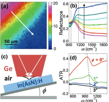
The ATR spectra were acquired at different positions, sepa-rated by 100 µm or 1 mm (see the insets in Figure 2a,b, respec-tively). In Figure 2a,b, we plot the signal as ATR =−log (IR/II), where IR and II are the intensities of the reflected and incident light beam, respectively. We observe that the frequency of the SPP resonance peak is nonhomogeneous over length scales of ≈1 mm (Figure 2b). This variation is likely to be caused by the inhomogeneity of the as-grown material[34] (see also Section S1 in the Supporting Information). The nonhomoge-neous N-content and defects in In(AsN) may induce a nonu-niform hydrogen incorporation. However, we note that the hydrogenation process is uniform: the standard deviation of the H-beam Gaussian profile (≈2.5 cm) is much larger than the sample size (≈0.4 cm). Plasmonic devices can be still developed on length scales where these variations are small (<100 µm, Figure 2a). We measure values of ωspp ranging from 890 to 950 cm−1 (970–1000 cm−1) for t = 0.3 µm (t = 1 µm). These are smaller than ωp and match well with those obtained by modeling the SPP dispersion for a single interface between air (ε1= 1) and the In(AsN):H epilayer ( ( )ε ω ε2 = 2∞−ω ωp2/( 2+igω)), see dashed red curve in Figure 1c and Table 1.
The dispersion of the SPP mode is given by ck
ω= || (ε1 +ε ε ε2)/ 1 2, where c is the speed of light in vacuum and k|| is the component of the wavevector parallel to the inter-face.[33] Figure 2c shows the dispersion calculated for g = 0 (dashed black curve) and g = 90 cm−1 (solid black curve). For
g = 0, the SPP dispersion approaches the surface plasmon fre-quency (green dot in Figure 2c) for infinite values of k||, i.e.,
ωsp=ω εp 2∞/(ε1 +ε2∞)<ωp (orange dot in Figure 2c). For a finite broadening g = 90 cm−1, the SPP dispersion broadens and approaches ωsp at finite k||. As indicated in Figure 2c, the SPP resonance can be excited if light from the Ge prism is incident at angles 14.5°< θ< 17°, consistent with the requirement for total internal reflection.
An air gap between the Ge prism and the In(AsN):H layer is required to achieve total internal reflection and thus observe the SPP mode. This can occur due to the natural tilting of the sample or can be induced intentionally. Figure 3a shows a color map of the integral of the reflectance intensity in the spectral range of the SPP mode. This reveals an intensity gradient, thus suggesting a natural tilting of the surface and the existence of an air gap between the Ge prism and the In(AsN):H epilayer. The blue areas in the color map correspond to regions with a larger air gap, thus leading to total internal reflection and the SPP resonance (Figure 3b). We estimate a small tilting of the surface at an angle φ* ≈ 0.5°. This corresponds to an air gap
tair of up to ≈0.9 µm,[35] consistent with the value obtained from the simulation of the ATR spectrum in Figure 1c (tair= 1 µm, dashed red curve).
[image:3.595.308.546.74.365.2]sample (Figure 3c,d): the SPP resonance tends to weaken and to blueshift with increasing φ. We attribute this behavior to the increase of the air gap with φ, thus leading to the expo-nential decay of the evanescent wave and a modified SPP ω–k|| dispersion. A similar behavior is observed in highly doped InAs epilayers. Figure 4 shows the ATR spectra for an InAs sample with t = 1.3 µm at tilted angles φ= 0°–3° (see also Section S2 in the Supporting Information).
2.2. Raman Spectroscopy of Plasma Modes
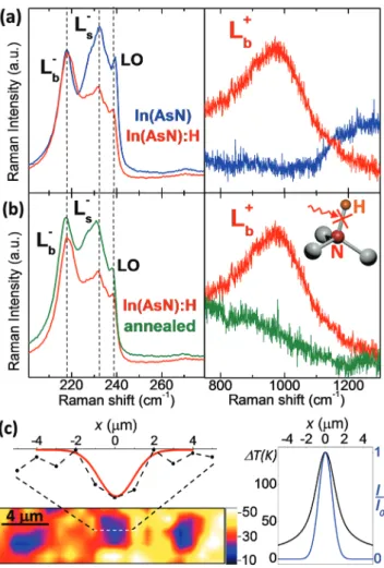
Further insights into the plasmonic effects were inferred from Raman spectroscopy studies. These were performed in the backscattering configuration with incident light of
wavelength λ = 633 nm. In Figure 5a, left panel, the com-parison of the Raman spectrum of In(AsN) (blue curve) with that of In(AsN):H (red curve) evidences a broad feature
ω =
− − −
L (s s 231 cm )1 between the TO (ωTO = 218 cm−1) and LO phonon frequency (ωLO = 239 cm−1). This feature weakens upon H-incorporation. The same comparison also shows the insurgence of a phonon–plasmon coupled mode, L+b, centered at 975 cm−1, in the Raman spectrum of In(AsN):H (red curve in Figure 5a, right panel).[25,27]
The frequencies of the phonon–plasmon coupled modes
±
Lb for bulk In(AsN):H and in the limit of wavevector k ≈ 0 are given by[36]
1
2 4
b p2 LO2 p2 LO2 2
p2 TO2
ω±=
(
ω +ω) (
± ω +ω)
− ω ω (1)The position of the L+b mode, which has a strong dependence on ne, corresponds to a plasma frequency consistent with that estimated from the reflectance spectra in the Brewster con-figuration (see Table 1). The Raman shift of the corresponding
−
Lb mode is expected to coincide with that of the TO mode
ω =− −
( b 218 cm )1 .
As regards the L−
s mode, it is well known that a 2D surface accumulation layer forms in InAs[37,38] and In(AsN).[31] For a layer extending over a typical length ls, the range of allowed wavevectors is Δk ∼ 2/ls, which can be comparable with the Thomas–Fermi screening wavevector. In this case, the surface LO-plasmon coupled mode, L−s, can be at a frequency interme-diate between ωTO and ωLO.[39–41] From the calculated disper-sion, we estimate that the measured position of the L−s mode corresponds to a surface accumulation layer with thickness ls≈ 2 nm (see Section S3 in the Supporting Information).
In summary, the Raman spectra reveal the “surface” L− s mode at ω =s− 232cm−1, the “bulk” L−b mode at ω =−b 218 cm−1, and the L+
b mode at ω =+b 975 cm−1.
2.3. Tuning Plasma Modes by Laser Annealing
To study the tunability of plasmonic effects, the In(AsN):H samples were photoannealed with a focused laser beam with
λ = 633 nm (Figure 5b). The light diffraction limit at this wavelength is given by the laser spot diameter d = 1.22λ/ NA ≈ 1 µm, where NA (= 0.8) is the numerical aperture of our Figure 3. a) Integrated intensity of the reflectance signal from 950 to
1150 cm−1 for the In(AsN):H sample with thickness t = 1 µm. b) Reflec-tance spectra in the ATR configuration acquired along the arrow in the color map. c) Sketch of the modified ATR setup: the sample is tilted by an angle φ relative to the horizontal support. This creates an air gap between the Ge prism and the In(AsN):H epilayer. d) ATR spectra at various angles
[image:4.595.115.479.573.684.2]φ= 0°–3°.
100× objective. The annealing was performed at impinging powers up to P = 15 mW and exposure times τ≥ 300 s. As shown in Figure 5b, following the laser annealing the intensity of the L−
s mode is almost fully restored to that of the In(AsN) sample (left panel) and the L+b feature disappears (right panel). This suggests the dissociation of the NH bond and local removal of hydrogen from the lattice (see Inset of Figure 5b, right panel), thus restoring locally the pristine conditions of as-grown In(AsN).
Figure 5c (bottom left panel) shows the Raman map of the
+
Lb intensity over three different positions of the sample that are laser annealed. Three clear minima in the intensity are seen, thus confirming a local quenching of the L+b mode. We fit the intensity distribution of the L+
b mode over the annealed spots with a Gaussian of full-width-half-maximum of ≈2 µm (top left panel), which is larger than the light diffraction limit
(≈1 µm). This broadening is attributed to a thermal effect:[42] we estimate that the laser beam causes a temperature rise of up to ΔT = 140 K that extends over a sample region wider than the laser spot (Figure 5c, right panel).[43] We note that that the annealing conditions used in our experiment do not cause any visible damage to the surface. In particular, atomic force micros-copy studies of the surface of In(AsN):H before and after the laser annealing (Section S4, Supporting Information) indicate that for the range of laser powers (P up to 15 mW) and expo-sure times (τ up to 15 min) required to quench the L+b mode, the laser annealing does not cause any topographic modification of the surface. Therefore, hydrogen-implantation followed by laser writing is a reproducible and nondestructive process that paves the way to patterning on a micrometric scale the In(AsN) plas-monic modes via a modulation of the material carrier density.
3. Conclusions
In summary, we demonstrated that the incorporation of hydrogen in the dilute nitride alloy In(AsN) with N-content of 1% induces a SPP mode at frequencies ωspp≈ 900–1000 cm−1, which correspond to MIR wavelengths λ ≈ 10–11 µm. We attribute the occurrence of this mode to the H-enhanced elec-tron density. The N-atoms play a key role in the incorporation of hydrogen: they trap the H-atoms, whose small size and high diffusivity in the host crystal enables an increase in the elec-tron density up to ne ≈ 1019 cm−3 near to the surface. A sim-ilar increase of carrier density could be achieved for different N-concentrations under appropriate hydrogenation condi-tions.[27] We demonstrated that plasmonic effects in In(AsN):H can be selectively suppressed on a micrometer scale by a local laser annealing. The dissociation of the NH bond by laser writing offers a viable route to large-scale device fabrication and a means to pattern the electron density and plasmonic proper-ties with micrometric resolution. The possibility to monitor the lateral size of the patterns, as well as the doping of the host crystal, could enable microscopic studies of plasmonic gratings and plasmonic phenomena near a surface, with potential for applications including detection of target gas fingerprints and molecular sensing in the MIR range. Compared to the tradi-tional doping of InAs during the growth, which requires wet chemical etching to realize plasmonic gratings, the postgrowth H-doping of In(AsN) has potential for engineering plasmonic properties via the selective hydrogen incorporation and/or removal by laser writing.
4. Experimental Section
[image:5.595.55.290.76.423.2]The nominally undoped dilute nitride In(AsN) epilayers were grown using a VG-V80H solid-source MBE reactor with a Vecco UNI-bulb radio frequency (RF) plasma nitrogen-source. In and Ga fluxes were provided by Knudsen thermal-effusion cells. The In(AsN) epilayers were grown at 450 °C using an RF power of 200 W and a nitrogen background pressure of 5 × 10⁻⁶ mbar. The layers were grown on 250 nm thick GaAs buffers on semi-insulating (1 0 0)-oriented GaAs substrates. In situ characterization was performed by reflection high energy electron diffraction. The as-grown In(AsN) epilayers were then hydrogenated using a Kaufman source under impinging H-dose DH = 3 × 10¹⁷ ions cm−2 at the Figure 5. a) Raman spectra showing the L−b, L−s, LO (left panel), and L+b
(right panel) modes in In(AsN) (blue curve) and In(AsN):H (red curve). b) Raman spectra showing the L−b, L−s, LO (left panel), and L+b (right
panel) modes in In(AsN):H before (red curve) and after (green curve) laser annealing. Inset: sketch of the dissociation of the NH bond due to laser excitation. c) Left: map of the L+b intensity after laser annealing
of three different spots, and profile of the L+b intensity along the dashed
temperature TH = 375 °C for 2 h. Under these conditions, the hydrogen penetrates to a depth of about ≈0.1 µm below the surface.[26]
The reflectance spectra in the Brewster configuration were acquired using a Hyperion 3000 microscope coupled to a Vertex 70 FTIR spectrometer with a Globar light source, a polarizer, a KBr beam splitter, and a deuterated triglycine sulfate (DTGS) detector. The absorption coefficient α< 105 m−1 at λ= 2–10 µm[44] gives an absorption length l > 10 µm. In the ATR configuration, a 20× ATR objective was used to focus the light beam through a Ge prism to a diameter d ≈ 100 µm. The absorption length in this case is significantly smaller than in the Brewster configuration.[33] The SPPs were excited in the Otto geometry, with a thin air gap between the Ge prism and the sample surface (Figure 3c). The air gap can appear due to a natural misorientation of the substrate or by using a controlled wedge. The light was detected using a mercury cadmium telluride detector. The ATR maps were obtained by using a focal planar array, with a spatial resolution of 2.5 µm at a wavelength
λ= 2.5 µm, and by integrating the reflectance intensity variation with respect to a baseline. Raman spectroscopy studies were performed using a He–Ne laser (λ= 633 nm), an XY linear positioning stage, a LabRAM optical confocal microscope system, and a spectrometer with 1200 grooves mm−1 gratings, equipped with a Si charge-coupled device; the laser beam was focused to a diameter d ≈ 1 µm using a 100× objective. An absorption length l ≈ 0.1 µm at λ= 633 nm was estimated.[45] The Raman spectra were measured at room temperature (T = 300 K) at a power P < 1 mW. The same experimental setup was used for local laser annealing experiments with powers up to P = 15 mW.
Supporting Information
Supporting Information is available from the Wiley Online Library or from the author. The data on which this manuscript is based are available as an online resource with digital object identifier (DOI) 10.17639/nott.324.
Acknowledgements
This work was supported by the Engineering and Physical Sciences Research Council [grant numbers EP/J015849/1, EP/J015296/1]; the EU Marie Sklodowska-Curie ITN-PROMIS [grant number 641899]; the French “Investment for the Future” Program [grant number EquipEx EXTRA, ANR 11-EQPX-0016]; the French ANR [grant number SUPREME-B, ANR-14-CE26-0015]; and the Occitanie region.
Conflict of Interest
The authors declare no conflict of interest.
Keywords
hydrogen, InAs, mid-infrared, plasmonics, semiconductors
Received: May 26, 2017 Revised: November 13, 2017 Published online:
[1] G. V. Naik, V. M. Shalaev, A. Boltasseva, Adv. Mater. 2013, 25, 3264. [2] P. R. West, S. Ishii, G. V. Naik, N. K. Emani, V. M. Shalaev,
A. Boltasseva, Laser Photonics Rev. 2010, 4, 795.
[3] F. Scotognella, G. Della Valle, A. R. Srimath Kandada, M. Zavelani-Rossi, S. Longhi, G. Lanzani, F. Tassone, Eur. Phys. J. B 2013, 86, 154.
[4] M. Henini, M. Razeghi, Handbook of Infrared Detection Technologies, Elsevier, Oxford, UK 2002.
[5] Z. Han, P. Lin, V. Singh, L. Kimerling, J. Hu, K. Richardson, A. Agarwal, D. T. H. Tan, Appl. Phys. Lett. 2016, 108, 141106. [6] M. J. Milla, F. Barho, F. González-Posada, L. Cerutti, M. Bomers,
J.-B. Rodriguez, E. Tournié, T. Taliercio, Nanotechnology 2016, 27, 425201.
[7] D. Li, C. Z. Ning, Opt. Express 2011, 19, 14594.
[8] F. B. Barho, F. Gonzalez-Posada, M. J. Milla, M. Bomers, L. Cerutti, T. Taliercio, Opt. Express 2016, 24, 16175.
[9] E. F. Schubert, Doping in III–V Semiconductors, Cambridge University Press, Cambridge, UK 1993.
[10] S. B. Zhang, J. Phys.: Condens. Matter 2002, 14, R881. [11] C. M. Wolfe, G. E. Stillman, Appl. Phys. Lett. 1975, 27, 564. [12] D. M. Luz, S. S. Makler, E. V. Anda, J. Phys. C: Solid State Phys. 1988,
21, 5149.
[13] A. Boltasseva, H. A. Atwater, Science 2011, 331, 290. [14] G. V. Naik, A. Boltasseva, Phys. Status Solidi RRL 2010, 4, 295. [15] G. V. Naik, A. Boltasseva, Metamaterials 2011, 5, 1.
[16] E. Sachet, C. T. Shelton, J. S. Harris, B. E. Gaddy, D. L. Irving, S. Curtarolo, B. F. Donovan, P. E. Hopkins, P. A. Sharma, A. L. Sharma, J. Ihlefeld, S. Franzen, J.-P. Maria, Nat. Mater. 2015, 14, 414.
[17] J. A. Schuller, R. Zia, T. Taubner, M. L. Brongersma, Phys. Rev. Lett. 2007, 99, 107401.
[18] A. J. Hoffman, L. Alekseyev, S. S. Howard, K. J. Franz, D. Wasserman, V. A. Podolskiy, E. E. Narimanov, D. L. Sivco, C. Gmachl, Nat. Mater. 2007, 6, 946.
[19] T. Taliercio, V. N. Guilengui, L. Cerutti, E. Tournié, J.-J. Greffet, Opt. Express 2014, 22, 24294.
[20] Y. Zhong, S. D. Malagari, T. Hamilton, D. Wasserman, J. Nanophotonics 2015, 9, 093791.
[21] E. Tokumitsu, Jpn. J. Appl. Phys. 1990, 29, L698.
[22] S. Law, D. C. Adams, A. M. Taylor, D. Wasserman, Opt. Express 2012, 20, 12155.
[23] T. D. Veal, L. F. J. Piper, P. H. Jefferson, I. Mahboob, C. F. McConville, M. Merrick, T. J. C. Hosea, B. N. Murdin, M. Hopkinson, Appl. Phys. Lett. 2005, 87, 182114.
[24] R. Kudrawiec, J. Misiewicz, Q. Zhuang, A. M. R. Godenir, A. Krier, Appl. Phys. Lett. 2009, 94, 151902.
[25] N. V. Kozlova, G. Pettinari, O. Makarovsky, N. Mori, A. Polimeni, M. Capizzi, Q. D. Zhuang, A. Krier, A. Patanè, Phys. Rev. B 2013, 87, 165207.
[26] A. V. Velichko, A. Patanè, M. Capizzi, I. C. Sandall, D. Giubertoni, O. Makarovsky, A. Polimeni, A. Krier, Q. Zhuang, C. H. Tan, Appl. Phys. Lett. 2015, 106, 022111.
[27] S. Birindelli, M. Kesaria, D. Giubertoni, G. Pettinari, A. V. Velichko, Q. D. Zhuang, A. Krier, A. Patanè, A. Polimeni, M. Capizzi, Semicond. Sci. Technol. 2015, 30, 105030.
[28] R. Trotta, A. Polimeni, M. Capizzi, Adv. Funct. Mater. 2012, 22, 1782.
[29] G. Ciatto, Hydrogenated Dilute Nitride Semiconductors – Theory, Properties and Applications, Pan Stanford Publishing, Singapore 2015.
[30] Basic Semiconductor Physics (Ed: C. Hamaguchi), Springer-Verlag, London 2006.
[31] A. Patanè, W. H. M. Feu, O. Makarovsky, O. Drachenko, L. Eaves, A. Krier, Q. D. Zhuang, M. Helm, M. Goiran, G. Hill, Phys. Rev. B 2009, 80, 115207.
[32] O. Drachenko, A. Patanè, N. V. Kozlova, Q. D. Zhuang, A. Krier, L. Eaves, M. Helm, Appl. Phys. Lett. 2011, 98, 162109.
[33] S. A. Maier, Plasmonics: Fundamentals and Applications, Springer, New York, USA 2007.
M. Henini, Q , Zhuang, A. Godenir, A. Krier, J. Appl. Phys. 2010, 108, 103504.
[35] We estimate the natural tilting of the epilayer by performing the ATR studies for different tilted angles of the sample relative to the horizontal support, i.e., φ= 0°, ±1°, etc. Since in both the φ= 0°
and φ=−1° configurations, the ATR spectra are the same, by taking into account that the Ge prism has a cylindrical symmetry, we deduce that the natural tilting of the epilayer is φ* ≈ 0.5°. From the diameter of the contact zone of the Ge prism, dGe= 100 µm, we thus estimate an air gap of up to ≈0.9 µm.
[36] E. D. Palik, J. K. Furdyna, Rep. Prog. Phys. 1970, 33, 1193.
[37] C. A. Mead, W. Q. Spitzer, Phys. Rev. Lett. 1963, 10, 471.
[38] P. D. C. King, T. D. Veal, C. F. McConville, J. Zúñiga-Pérez, V. Muñoz-Sanjosé, M. Hopkinson, E. D. L. Rienks, M. F. Jensen, P. Hofmann, Phys. Rev. Lett. 2010, 104, 256803.
[39] R. A. Cowley, G. Dolling, Phys. Rev. Lett. 1965, 14, 549. [40] S. Buchner, E. Burstein, Phys. Rev. Lett. 1974, 33, 908.
[41] Y. B. Li, I. T. Ferguson, R. A. Stradling, R. Zallen, Semicond. Sci. Technol. 1992, 7, 1149.
[42] M. Lax, J. Appl. Phys. 1977, 48, 3919.
[43] This large increase of T is reached at relatively low powers due to the high absorption coefficient (α≈ 107 m−1 at λ= 633 nm) and low thermal conductivity (K = 27 W m−1 K−1 at T = 300 K) of In(AsN). [44] J. R. Dixon, J. M. Ellis, Phys. Rev. 1961, 123, 1560.