A Performance ofModern Dynamic Random Access Memory: A Systematic Review
P. Lachi Reddy1, Dr.Phool Singh Chouhan2, Dr.Senthilkumar A3
Department of Electronics and Communication Engineering 1,2,3
OPJS University, Churu (Rajasthan) Abstract
The paper depicts the deep study of DRAM. The audit talks about fundamental presentation of Measure, DRAM engineering and its bolster hardware. The paper likewise concentrates on the study of four transistor DRAM cell, two transistor DRAM cell and one transistor DRAM cell. Perused and compose operations of various sorts of Drams are clarified with help of control flag waveform. The examination between two fundamental sorts of recollections i.e. SRAMand DRAM is additionally examined in the paper. This paper additionally means to study different fields of application where DRAM can be utilized. The power utilization is a principle concern nowadays for long operational life. Albeit various sorts of procedures to diminish the power scattering has been developed. A standout amongst the most received strategy is to lower the supply voltage inthese paper static random axismemory parameters like low power, superior circuit and attributes and applications.
Key words —SRAM, DRAM, CMOS
INTRODUCTION
There are numerous variations of DRAMs, for
example, Asynchronous DRAM, Synchronous
DRAM (SDRAM), and Double Data Rate (DDR)
SDRAM and so forth. Every piece in a DRAM is
put away in only one capacitor inside the silicon.
Because of the auxiliary effortlessness (one
transistor and one capacitor for every piece) of
DRAMs, they can achieve high thickness bringing
about vast limits. On the drawback, similarly as
were capacitors, these DRAM capacitors lose
charge over a timeframe.
A common DRAM requires one revive cycle each
15.6 µs [1]. Amid the revive operation, the last
opened column is shut before the invigorate line
is opened. The processor gets to the DRAM
memory for bringing data and guidelines in case
of a store miss, however, this bring is slowed
down while DRAM auto revive is in advance. In
this manner, the reaction time of a DRAM access
rely on upon the purpose of time memory is
gotten to by the processor in respect to a DRAM
revive.
Implanted control systems sent in security basic
situations or process plants, then again, by and
large force more stringent planning consistency
prerequisites that are inclined to be abused
because of DRAM revive delays. From
plants to car subsystems, for example, ABS,
system rightness reaches out from the
conventional info/yield connections to due dates.
Modern DRAM device data rates and row cycle
times are scaling at different rates with each
successive generation of DRAM devices. As a
result, the performance characteristics of
modern DRAM memory systems are becoming
more difficult to evaluate at the same time that
they are increasingly limiting the performance of
modern computer systems [2]. utility and
flexibility of the Request Access Distance
analytical framework, systems with differing
organizations and timing parameters are used to
study the impact of different row cycle times,
device data rates, data burst lengths, tFAW power
constraints, tDQS rank-to-rank data bus switching
time, the number of banks and the number of
ranks in the memory system.
The performance characteristics of DRAM
memory systems depend on workload specific
characteristics of access rates and access
patterns. In the Request Access Distance
analytical framework, input traces are driven at
saturation rates so that the effects of processor
performance can be factored out from memory
system performance. Despite the fact that the
workload traces are driven at saturation rate of
the respective memory systems, the
workload-specific request access patterns remain
important in the analysis of DRAM memory
system performance.
A REVIEW ON DRAM
Dynamic Random Access Memory (DRAM)
gadgets are utilized as a part of an extensive
variety of hardware applications. In spite of the
fact that they are delivered in many sizes and
sold in an assortment of bundles, their general
operation is basically the same. Measures are
intended for the sole reason for putting away
information. The main legitimate operations on a
memory gadget are perusing the information put
away in the gadget, composing (or putting away)
information in the gadget, and reviving the
information intermittently [3]. To move forward
effectiveness and speed, various techniques for
perusing and composing the memory have been
developed. Dynamic random axis memory
(DRAM) incorporated circuits (ICs) have existed
for more than a quarter century. Measures
developed from the most punctual 1-kilobit (Kb)
era to the late 1-gigabit (Gb) era through
advances in both semiconductor process and
circuit outline innovation. Enormous advances in
process innovation have significantly decreased
element estimate, allowing ever more elevated
amounts of mix. These increments in joining have
been joined by major enhancements in segment
respect guarantee that general procedure
Innovation changes, nonetheless, are not
constrained to semiconductor handling. A
considerable lot of the advances in process
innovation have been joined or empowered by
advances in circuit outline innovation [4].
Atanassov and Puschner inspected the impact of
DRAM empower on the execution time of
nonstop endeavors. For their goal course of
action, they figure the most outrageous possible
augmentation of execution time due to fortifies
to be 2.13%. Using their informative technique,
we figured the most critical situation execution
time for the target outlines we are using as a
piece of our trials to be around 2%.
A. R. Lebeck et al. (2000)the makers propose
control careful page assignment counts for DRAM
control organization. They expect support in
memory controller for fine grained bank level
power control, and exhibit that their task
figuring’s give more noticeable open entryways
for setting memory in low power modes. In the
makers propose an OS level approach, where the
OS keeps up tables that guide frames onto the
memory banks they have their memory allotted
in. This allows the OS to logically move unutilized
DRAM banks into low power modes.
The makers inH.-L.Li et al. (2000) propose NAND
streak based page store, which diminishes the
measure of DRAM required for system memory.
These results in imperativeness viability on
account of lower power usage and higher
thickness of NAND blast appeared differently in
relation to DRAM. Additionally SPICE
investigation demonstrated that if charge were
gathered at two hubs on inverse legs of the
circuit, the edge for bombshell could be
considerably decreased Fail-tally change by
conjuring the read help include (lower bend
contrasted with center bend). Comes about
additionally demonstrate that excessively
forceful of a SA setting can essentially increments
come up short tally (high bend).
SA-gadget bungle triggers the compose back of
inverse information to cells into equal parts
chose segments. Impacts of the compose help
are likewise noted in the equipment. A slight
increment in come up short tally is watched for
cells sharing the lower compose help voltage
amid the compose operation. This equipment
was prepared with powerless PFETs and
increments in come up short number are
ascribed to diminished information maintenance.
While this equipment did not demonstrate a
positive advantage for the compose help, it
highlighted a critical restriction; the compose
help advantage at low voltage clashes with the
fundamental prerequisite for cell information
maintenance. Come up short number decreases
are normal with lower PFET-gadget Vt. The 32Mb
DRAM ARCHITECTURE
Measure chips are substantial, rectangular
varieties of memory cells with bolster rationale
that is utilized for perusing and composing datain
the exhibits, and revive hardware to keep up the
honesty of put away information.
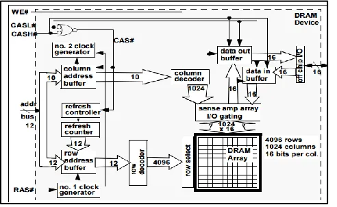
DRAM Organization:
Inside, the variety of DRAM stockpiling cells in
Figure 1 is composed as 4096 lines, 1024 sections
for every line, and 16 bits of information for
every segment. In this gadget, every time a line
get to happens, a 12 bit address is set on the
address transport and the line address strobe
(RAS) is attested by an outer memory controller.
Inside the DRAM gadget, the address on the
address transport is supported by the column
address cradle, and then sent to the line decoder.
The column address decoder then acknowledges
the 12 bit address and chooses one of 4096 lines
of capacity cells [5].
Figure 1: Mbit fast page mode DRAM Device
Addressable unit of memory in this gadget and
each segment get to that takes after the Row get
to would usually read or make 16 bits out of
information from a comparative line of DRAM.
The FPM DRAM gadget allows each 8 bit half of
the 16-bit segments to be gotten to uninhibitedly
utilizing separate portion get to strobe high
(CASH) and Column Access strobe low (CASL)
signals [6]. The FPM DRAM gadget also keeps the
address of the following segment that ought to
be strengthened, so when the memory controller
confirms another restore request to the DRAM
gadget, the line conveyance to be stimulated can
be stacked from the internal fortify counter
instead of stacking an alternate line address from
the off-chip address transport. Moreover, stick
utilize has reliably been restrictive on DRAM
gadgets. Likewise, show day DRAM gadgets move
information onto and off of the gadget through a
game plan of bi-directional information yield pins
connected with the system.
Memory Arrays
Memory clusters are organized in lines and
sections of memory cells called word lines and bit
lines, separately. Each memory cell has a
remarkable area or address characterized by the
Memory Cells
A DRAM memory cell is a capacitor that is
charged to create a 1 or a 0. Throughout the
years, a few distinct structures have been utilized
to make the memory cells on a chip. In today's
innovations, trenches loaded with dielectric
material are used to make the capacitive
stockpiling component of the memory cell.
Bolster Circuitry
The memory chip's bolster hardware allows the
client to peruse the information put away in the
memory's cells, compose to the memory cells,
and revive memory cells. This hardware by and
large incorporates:
Sense speakers to open up the flag or
charge identified on a memory cell.
Deliver rationale to choose lines and
sections.
Push Address Select (RAS) and Column
Address Select (CAS) rationale to hook
and resolve the line and section delivers
and to start and end read and compose
operations.
Perused and compose hardware to store
data in the memory's cells or read what is
put away there
Direct RDRAM System Topology
One memory system with a system topology
drastically unique in relation to the
traditional DRAM memory system topology is
the Direct RDRAM memory system. Direct
RDRAM gadgets are demonstrated associated
with a solitary Direct RDRAM memory
controller. Figure 2 demonstrates that in a
Direct RDRAM memory system, the DRAM
gadgets are associated with an all-around
coordinated system of interconnects where
the timing system, the information transport
and the command transports are all way
length coordinated by plan [8].
The advantage of the all-around coordinated
interconnection system is that flag skew is
insignificant by outline and electrical flagging
rates in the Direct RDRAM memory system
can be expanded to higher frequencies than a
memory system with the great memory
Figure 2: topology of a generic direct RDRAM
memory system
Examination of DRAM w.r.t. SRAM
SRAM and DRAM are two fundamental sorts of
RAM. The term SRAM stands for Static Random
Access Memory and Measure stands for Dynamic
Random Access Memory. SRAM is comprised of
transistor and DRAM is comprised of capacitor.
Subsequently a SRAM stores the paired piece
advice of voltage; 5v speak to 1 and 0v speaks to
0. Measure stores twofold piece in type of
charge; nearness of charge speak to 1 and
nonappearance of charge (release) speak to 0.
The charge on the capacitor actually spills in
couple of milliseconds. In this way a DRAM
should be revived (called invigorating a Measure)
occasionally for the most part every 2
milliseconds. For this, a DRAM needs an
uncommon reviving circuit. Measures are less
expensive than SRAMs and have high pressing
thickness. A DRAM devours less power than a
SRAM. They have lower speed than SRAMs. Less
expensive DRAM is utilized as a part of primary
memory while SRAM is generally utilized as a part
of store memory [9].
Measure versus-Logic Optimized Process
Technologies
One clearly unavoidable example in
semiconductor amassing is the stroll toward
blend. As the semiconductor manufacturing
industry dutifully fulfills Moore's Law, each
duplicating of transistors allow arrangement
creators to pack more method of reasoning
equipment or more DRAM stockpiling cells onto a
flag bit of silicon. Regardless, the semiconductor
business has so far all things considered
contradicted the blend of DRAM and method of
reasoning onto a comparative silicon gadget for
various particular and money related reasons
specific issues that have kept away from
generous scale compromise of justification
CONCLUSION
The paper completely clarifies the design of
DRAM, hardware and cells of DRAM with their
working operation. Examination amongst SRAM
and DRAM is additionally being made on the
premise of their circuit, cost, charge thickness,
and applications. At the point when SRAM as a
result of its high cost must be utilized as reserve
memory while low cost Measure utilized as a
principle memory.
REFERENCES
1. P. Atanassov and P. Puschner (2006),
“Impact of dram refresh on the
performance time of real-time tasks,” in
Proc. IEEE International Workshop on
Application of Reliable Computing and
Communication, Dec. 2001, pp. 29–34.
2. A. R. Lebeck et al. Power aware page
allocation. SIGOPS Oper. Syst. Rev.,
34(5):105–116, 2000.
3. P.R. Dark and R.G. Meyer (2003), Analysis
and Design of Ana log Integrated Circuits,
third release, New York, NY: John Wiley
and Sons, Inc., 1993.
4. B. Ruler (2005), Semiconductor
Memories, second release, New York, NY:
John Wiley and Sons, Inc.,
5. R. J. Pastry specialist, H. W. Li, and D. E.
Boyce (2002), CMOS: Circuit Design,
Layout, andSimulation. Piscataway, NJ:
IEEE Press. PowerCircuits," Proceedings
of International Conference of PC Aided
Design, pp. 62-65, 1995.
6. NahidRahman, B.P. Singh (2005) “Design
of Low Power Sram Memory Using 8t
Sram Cell” International Journal of
Recent Technology and Engineering
(IJRTE), pp123-127, 2013
7. ManpreetKaur, Ravi Kumar Sharma
(2001) “COMPARATIVE PARAMETRIC
ANALYSIS FOR STABILITY OF 6T AND 8T
SRAM CELL” International Journal of
Advances in Engineering & Technology,
pp 503-514, 2012
8. Archnabai (2003) “SRAM CELL MODELING
FOR READ STABILITY AND WRITE ABILITY”
International Journal of Emerging
Technologies in Computational and
Applied Sciences (IJETCAS), pp26-31,
2012
9. Sapna Singh, NehaArora,
MeenakshiSuthar and Neha Gupta (2002)
DIFFERENT SRAM CELL STRUCTURES AT
DIFFERENT TECHNOLOGIES” International
Journal of VLSI design & Communication
Systems (VLSICS), pp97-109, 2012.
10. P. Atanassov and P. Puschner (2005),
“Impact of dram refresh on the
performance time of real-time tasks,” in
Proc. IEEE International Workshop on
Application of Reliable Computing and
Communication, Dec. 2001, pp. 29–34.