COMPARATORSUSING 180NM TECHNOLOGY
1
Sweta Kumari ,
2Sampath Kumar V
1,2
Department of Electronics Engineering, JSS Academy of technical education, Noida, (India)
ABSTRACT
In todays world, high speed and low power era is an increasing demand of a High Speed Comparator for ADC, DAC and various other applications in an analog and digital domain. This paper represents a comparative study of three types of dynamic latched comparators in terms of offset voltages, speed , stability and power working in 180nm CMOS technology. The accuracy of comparators, which is defined by its offset, along with power consumption, speed is of keen interest in achieving overall higher performance of ADCs. This can be achieved by new comparator latch which not only gives better stability with reduced offset voltage but also minimizes the
propagation delay and power. Simulation results illustrates the superiority of new comparator latch over
conventional latch-type comparator as offset voltage is reduced to 42% in 180nm and propagation delay
reduced to 53% while again simulating in 100nm then to 180nm which shows enhancement of speed .
Keywords: ADC, CMOS Dynamic Latch Comparator, Charge Sharing Topology, High Speed, Low
Power, Propagation Delay, Offset Voltage.
1. INTRODUCTION
In today’s world, where demand for portable battery operated devices is increasing, a major thrust is given
towards low power methodologies for high resolution and high speed applications. Due to fast-speed, low-power consumption, high-input impedance and full-swing output, CMOS dynamic latched comparators are very attractive for many applications such as high-speed analog-to-digital converters (ADCs), memory sense amplifiers (SAs) and data receivers. Comparators are most probably second most widely used electronic components after operational amplifiers in this world. Comparators are known as 1-bit analog-to digital converter and for that reason they are mostly used in large abundance in A/D converter. There are number of comparator design techniques for use in parallel A/D converters that are implemented in BiCMOS and CMOS VLSI technologies.
Fig1. Block Diagram of High-Speed Voltage Comparator
The main drawback of pre-amplifier based comparators that it consume more static power and reduced gain due to varying technology scale, and latch comparator without pre-amplifier stage is desirable with using digital calibration technique.Therefore, for the high-speed lowpowerCMOS applications, a dynamic comparator withoutpre-amplifier is highly desirable .
II WIDELY USED CONVENTIONAL LATCH-TYPE COMPARATOR
The conventional dynamic latched comparators use positivefeedback mechanism with one pair of back-to-back cross coupled inverters (latch) to convert a small input-voltageoutput swing, and no static power consumption as shown in Fig 1: This circuit has the advantage of good robustness against noise and mismatch but suffers from high supply voltage due to many stacked transistors.
III MODIFIED COMPARATOR LATCH
The modified comparator latch design as shown in Fig 3 [2] is different from the conventional circuit by replacing a new latch for reduced delay and offset voltage. This comparator requires both the clock signals and the highly accurate timing relationship for its optimal operation.
Fig2.Widely Used Conventional Latch-Type Comparator Fig2
Modified Comparator Latch
However, a rail to rail output swing is produced with no static power dissipation. In addition, the modified designed comparator is free from indirect influence of the parasitic capacitances of the input transistors to the output nodes.
IV NEW COMPARATOR LATCH
The new comparator latch as shown in Fig4.[3] based on charge sharing topology which combines the best
reference voltage, Vref, then the output results willbe a “1” and if the input voltage is less than reference
voltagethen the output voltage of the comparators produces output of“0.”
Fig4. New Comparator Latch
V SIMULATION RESULT
Design has been simulated in 180nm and 100nm for propagation delay on different inputs (mV) to show improvement in speed. Power analysis,DC analysis and AC analysis in 180nm to show the new comparator latch minimum offset voltage and better stability than other two comparators For both the technology width of both nmos and pmos are same i.e. Wn=3um and Wp=6um.
5.1 Analysis of Delay
Propagation delay can be defined as at how much speed amplifiers respond with applied input..
Propagation Time Delay=Rising Propagation Delay Time + Falling Propagation Delay Time/2 Equation (1) Design is faster as the delay reduces in the circuit..Below are given the transient response of new comparator latch in 180nm and 100nm .
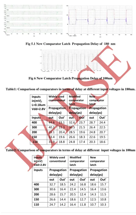
Fig 5.1 New Comparator Latch Propagation Delay of 180 nm
Fig 6 New Comparator Latch Propagation Delay of 100nm
Table1: Comparison of comparators in terms of delay at different input voltages in 180nm.
Inputs
in(mV),
L=0.18um
Vdd=2.8V
Widely used conventional Modified comparator latch New comparator latchPropagation
delay(ps)
Propagation
delay(ps)
Propagation
delay(ps)
Inputs
out
Out’
out
Out’
out
Out’
400
44.6
23.1
32.6
23.7
28.7
24.4
300
40.1
22.3
30.5
21.5
26.4
22.5
200
35.1
20.4
28.5
19.6
24.8
20.7
150
33.4
19.6
26.6
18.3
22.6
19.5
110
31.9
18.8
24.8
17.4
20.3
18.6
Table2: Comparison of comparators in terms of delay at different input voltages in 100nm
Inputs in(mV) Vdd=2.8V Widely used conventional Modified comparator latch New comparator latch
Inputs
Propagation
delay(ps)
Propagation
delay(ps)
Propagation
delay(ps)
out
Out’ out
Out’
out
Out’
Power dissipation is a measure of the rate at which energyis dissipated or lost , from an electrical system. P= Idd .VddEquation(2)
Table3: Comparison of comparator design in terms of Total power dissipation
Comparator design
L=0.18um,Vdd=2.8V
Total Power
Dissipation in
(Watts)
Widely used
Conventional latch-type
comparator
5.29E-09
Modified Comparator
latch
3.08E-09
New Comparator
latch
2.25E-09
Fig7.Graphically Representation of Total Power Dissipation
From the above Table3 and graphical Fig7. it is easily concluded that new comparator latch has less total power dissipation less.
5.3 Analysis of DC Offset Voltage
: Offset voltage is nothing just the distance between theorigin and the
output .Fig8. DC Response of Conventional Comparator In 180nm
Total Power Dissipation in (Watts)
Table4: Comparison of comparator design in terms of dc offset voltage
`Comparator design Dc output offset voltage(mV) L=0.18um ,Vdd=2.8V OUT OUT’ Conventional comparator 63.243 35.087 Modified Latch
comparator
40.143 32.087
New comparator latch 26.248 24.609
So from the above Table4 it is concluded that new comparator latch has less dc offset voltage than conventional.
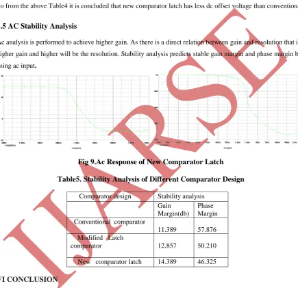
5.5 AC Stability Analysis
Ac analysis is performed to achieve higher gain. As there is a direct relation between gain and resolution that is higher gain and higher will be the resolution. Stability analysis predicts stable gain margin and phase margin by using ac input.
Fig 9.Ac Response of New Comparator Latch
Table5. Stability Analysis of Different Comparator Design
Comparator design Stability analysis Gain
Margin(db)
Phase Margin Conventional comparator
11.389 57.876 Modified Latch
comparator 12.857 50.210
New comparator latch 14.389 46.325
VI CONCLUSION
The new comparator latch shows better performance in terms of stability, offset voltage ,power and minimum
propagation delay over other designs. Therfore, this design is suitable for high speed and low power ADCs.
VII ACKNOWLEDGMENTS
The authors wish to thank Professor SampathkumarVand the anonymous reviewers for their constructive
[2] Raja Mohd . Noor Hafizi Raja Daud ,Mamun Bin IbneReaz, and LabonnahFarzana Rahman ,” Design and Analysis of Low Power and High Speed Dynamic Latch Comparator in 0.18μm CMOS Process”, IJIEE Vol. 2,
No. 6 ,pp. 944-947, November 2012.
[3] AjayVishwakarma, SwetaSahu, Ravi Vishwakarma and RichaSoni , ”Different Parameter Analysis of CMOS Charge Sharing Latch Comparator using 90nm Technology”, IJCA (0975 – 8887) Volume 63– No.11, pp.1-6, February 2013.