Communication-Centric Debug of
Systems-on-Chip using
Networks-on-Chip
Master thesis
March - August 2006
Report number: 069.020/2006
Author Supervisors
R. van Steeden Dr. ir. H.G. Kerkhoff (University of Twente)
Communication-Centric Debug of
Systems-on-Chip using
Networks-on-Chip
Master thesis
March - August 2006
Report number: 069.020/2006
CADTES SOC Architectures and Infrastructure Faculty of Electrical Engineering
NXP Semiconductors University of Twente
High Tech Campus 5 P.O. Box 217
5656 AE Eindhoven 7500 AE Enschede
The Netherlands The Netherlands
Author Supervisors
R. van Steeden Dr. ir. H.G. Kerkhoff (University of Twente)
Title: Communication-Centric Debug of Systems-on-Chip using Networks-on-Chip
Author(s): Remco van Steeden
Reviewer(s): Hans Kerkhoff, Bart Vermeulen
Technical Note: TN-2006-01234
Additional Numbers: Subcategory:
Project: Æthereal
Customer: Philips Research
Keywords: Communication-Centric, Debug, System-on-Chip, Network-on-Chip, Æthe-real
Abstract: This report explores the possibilities of combining debug methodologies and communication-centric design using NoCs. It also describes an implemen-tation of a debug architecture for the Philips Æthereal NoC, which is fully integrated in the Æthereal design flow.
Conclusions: Networks-on-Chip emerge as the new type of interconnect for next-generation systems-on-chip. They overcome the upcoming deep sub-micron effects, the increasing design complexity and the lack of scalability of busses. However NoCs can also assist in SoC debug as this report shows.
Looking at the communication of SoCs helps the debugging proces of prototype ICs. Raising the abstraction level from bits to transactions make it easier to interpret and compare what happens inside the NoC with a software transaction level model.
The proposed debug architecture and strategy can speed up the localiza-tion of erroneous IP cores and the time at which errors occur. Subsequently the malfunctioning IP core can be stopped at the right moment using the breakpoint hardware added to the NoC. Using the IP cores’ debug facilities and the controlled data supply from the NoC side, the error can then be found more quickly.
Contents
Preface 1
1 Introduction 3
1.1 Motivation . . . 3
1.2 Objective . . . 3
1.3 Related Work . . . 4
1.4 Structure . . . 4
2 Network-on-Chip 5 2.1 Introduction . . . 5
2.2 Æthereal NoC . . . 7
2.3 Æthereal Network Interface . . . 9
2.4 The Æthereal Router . . . 10
2.5 DTL Protocol . . . 11
3 Debug 13 3.1 Introduction . . . 13
3.2 Debug Strategy for SoCs using NoCs . . . 14
3.3 Debug Requirements for SoCs using NoCs . . . 15
3.3.1 Stop Operation . . . 17
3.3.2 Dump and Recover State . . . 17
3.3.3 Single Step and Continue Operation . . . 18
4 Debug Architecture Design 21 4.1 Overview . . . 21
4.2 Choices . . . 22
4.2.1 Introduction . . . 22
4.2.2 Stop Signal Distribution . . . 22
4.2.3 Protocol Adapter . . . 24
4.3 Stop Module . . . 24
4.4 Core-based Scan Architecture . . . 28
5 Debug Architecture Implementation 29 5.1 Overview . . . 29
5.2 Clock Control Slice . . . 30
5.3 Breakpoint Hardware . . . 30
5.4 Stop Module . . . 31
TN-2006-01234 Philips Restricted
6 Results 33
7 Conclusions and Future Work 37
7.1 Conclusions . . . 37 7.2 Future Work . . . 37
References 41
A Clock Control Slice Implementation 43
B Breakpoint Hardware Implementation 45
C Stop Module Implementation 47
D Protocol Adapter Implementation 49
E Æthereal Design Flow Changes 51
F Getting Started 53
Preface
This master’s thesis report concludes my education in electrical engineering at the University of Twente, the Netherlands. The project Communication-Centric Debug of Systems-on-Chip using Networks-on-Chipwas carried out from March till August 2006 at the IC Design / Digital Design & Test department of Philips Research Laboratories Eindhoven, the Netherlands, under the supervision of:
• Bart Vermeulen (NXP Semiconductors, SOC Architectures and Infrastructure)
• Kees Goossens (NXP Semiconductors, SOC Architectures and Infrastructure)
• Martijn Bennebroek (Philips Research, IC Design Group)
• Hans Kerkhoff (University of Twente, CADTES)
I would like to thank all of them for providing me this project, I really enjoyed working on it. Our discussions have broaden the view of certain problems and possibilities, which definitely contributed to the success of this project. Also the help of Bart with respect to debug and the integration with Incide was of great value.
Besides my supervisors I would like to thank Martijn Coenen for all his technical support regarding the Æthereal network-on-chip and the Æthereal design flow.
El Puerto de Santa María, October 1, 2006
Section 1
Introduction
This chapter first treats the motivation behind and the objective of this master thesis project in 1.1 and 1.2 respectively. Related work in the area of system-on-chip debug is summarized in 1.3 and the structure of this report is given in 1.4.
1.1
Motivation
Modern integrated circuits consist of a lot of Intellectual Property (IP) cores, like processor cores, memory blocks, peripherals, I/O resources and interconnects. Until now, the intercon-nects were mostly (bridged) busses and point-to-point connections. However with the increasing complexity of System-on-Chips (SoCs), the upcoming Deep Sub-Micron (DSM) effects and a lack of scalability, these busses become a bottleneck in next-generation chips.
A solution to this interconnect problem is a Network-on-Chip (NoC) [1, 2, 3, 4, 5, 6, 7]. A Network-on-Chip is a packet-switched network consisting of Routers (Rs) and Network Inter-faces (NIs). It allows IP cores to communicate with each other in a parallel manner and separates computation from communication.
Network-on-chip introduces new possibilities for debugging systems-on-chip. Debug is nec-essary because first-time-right SoC designs are still an utopia. An increasing number of cores and components within cores cause that, despite all the Computer Aided Design (CAD) tools and the reuse of cores, hardly any prototype chip returns without errors. Errors include incorrect functional timing of signals, incorrect hardware design, incorrect programming of hardware (e.g. wrong addresses, registers or read/write pointers) and incorrect scheduling of actions (resulting in e.g. data loss).
Traditional debug is done from a core-based perspective. Philips wanted to explore the pos-sibilities of combining debug methodologies and communication-centric design using networks-on-chip. It is believed that this integration will bring significant advantages in terms of shorter debug-time-to-root-cause and shorter time-to-market.
1.2
Objective
TN-2006-01234 Philips Restricted
Goals of the project:
• Defining the requirements and possibilities for communication-centric debug.
• Implementing a concept in VHDL.
• Integrating the concept with the Æthereal design flow.
• Demonstrating the capabilities of the implemented concept by means of a simulation.
1.3
Related Work
In the field of network-on-chip a lot of research is going on [8], however only Arteris is offering a commercial solution [9] at the moment.
Present solutions for system-on-chip debug are all core-based, e.g. ARM’s CoreSight [10] and DAFCA’s Flexible Silicon Debug Infrastructure [11]. Within Philips also a core-based ap-proach is being used [12].
As far as I know there are no communication-centric debug solutions (using networks-on-chip) for systems-on-chip yet. There are however some articles about monitoring services for networks-on-chip [13, 14, 15, 16, 17]. Also there is an article about the verification implications of bringing communication networks on chip [18].
1.4
Structure
The structure of this report is as follows:
• Chapter 2: An introduction to network-on-chip, the basics of the Æthereal NoC and Philips’ DTL protocol are treated.
• Chapter 3: An introduction to debug and a definition of the requirements for communication-centric debug using NoCs are given.
• Chapter 4: The design of the debug architecture is presented and the choices which are made to come to this design are discussed.
• Chapter 5: This chapter focuses on the implementation details of the design.
• Chapter 6: The results obtained with the implementation are presented.
Section 2
Network-on-Chip
This chapter introduces the network-on-chip concept (2.1), discusses the Æthereal NoC (2.2) consisting of the Æthereal network interface (2.3) and the Æthereal router (2.4) and treats the Philips’ DTL communication protocol (2.5).
2.1
Introduction
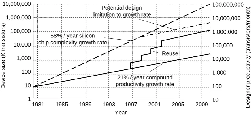
The prediction of Gordon Moore in 1965 that the transistor density of semiconductor chips would double every 18 months still holds true. Designers can not keep pace with the increas-ing design complexity which results in a design productivity gap between the chip complex-ity growth (doubling every 18 months) and the productivcomplex-ity growth (doubling roughly every 4 years), see Figure 2.1. A possible solution to this problem is reuse of IP cores on a chip. However as Figure 2.1 shows, this is not sufficient. Platform-based design is needed, where not only the IP cores are reused but also the communication, test and debug infrastructure and environment [19].
1981 1985 1989 1993 1997 2001 2005 2009 Year
10,000,000
1,000,000
100,000
10,000
1,000
100
10
1
100,000,000
10,000,000
1,000,000
100,000
10,000
1,000
100
10
Device si
ze (K transistors)
Desi
gner producti
vity (transistors/month)
Reuse Potential design
limitation to growth rate
21% / year compound productivity growth rate 58% / year silicon
chip complexity growth rate
Figure 2.1: Design productivity crisis: the divergence of potential design complexity and de-signer productivity (Source: Sematech, 1995).
TN-2006-01234 Philips Restricted
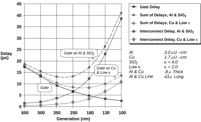
effects. The integration of an ever-increasing number of transistors on a chip leads to smaller gate delays but also to bigger wire delays, see Figure 2.2. With increasing operating frequencies the propagation delay of busses will exceed the clock period [2]. Traditional busses and point-to-point connections become a bottleneck in next-generation chips because of these DSM effects, the productivity gap and a lack of scalability.
0 5 10 15 20 25 30 35 40 45
650 500 350 250 180 130 100
Generation (nm)
Delay Al
Cu SiO2 Lowκ Al & Cu Al & Cu Line
3.0 –cm 1.7 –cm
κ = 4.0
κ = 2.0 .8 Thick 43 Long
Interconnect Delay, Cu & Low κ Interconnect Delay, Al & SiO2 Sum of Delays, Cu & Low κ Sum of Delays, Al & SiO2 Gate Delay
(ps)
Gate wi Cu & Low κ Gate wi Al & SiO2
Gate
Figure 2.2: Calculated gate and interconnect delay versus technology generation illustrating the dominance of interconnect delay over gate delay as feature sizes approach 100 nm (Source: National Technology Roadmap for Semiconductors, 1997).
A new kind of interconnect, called network-on-chip, can solve the upcoming problems. A network-on-chip is a packet-switched network consisting of routers and network interfaces, see Figure 2.3 for a comparison between a traditional bus system and a NoC. IP cores can commu-nicate with each other by sending messages. The network interfaces packetize/depacketize the messages and send/receive them to/from the switching fabric, which routes packets from source to destination.
A Network-on-Chip has the following properties:
• It separates computation (IP cores) from communication (NoC).
• It has predictable physical and electrical properties.
• It supports standard communication interfaces.
• It allows for parallel communication.
• It can be dynamically reconfigured.
• It is scalable.
R R
R R
NI
NI
NI
NI
NI NI NI NI
IP
IP IP
IP
IP IP
IP IP
NoC
IP
IP IP
IP
Bus 1 Bus 2
IP
IP IP
IP Bridge
(a) (b)
Figure 2.3: Traditional bridged bus system (a) and an example of a network-on-chip (b).
2.2
Æthereal NoC
The Quality of Service (QoS) offered by a network-on-chip is of great importance, however services also have their costs in terms of speed, area and power consumption [20]. Æthereal, Philips’ network-on-chip solution [21, 22, 23], aimes to offer Guaranteed Services (GSs). GSs need resource reservation and in order to increase resource utilization, Æthereal also imple-ments Best Effort Services (BESs). GSs serve critical communication (e.g. real-time or stream-ing data), called Guaranteed Throughput (GT) traffic. BESs serve non-critical communication, called Best Effort (BE) traffic. For GT communication, Æthereal provides guaranteed through-put, latency, jitter and in-order uncorrupted delivery. For BE communication latency can be es-timated, and in case of a fair scheduler and a deadlock-free network it can also be bounded [21].
In Æthereal, communication is performed on the basis of connections (GT or BE). A connection is always between two or more Network Interface Ports (NIPs); one Master NIP (MNIP) at the side of the producer IP core and one or more Slave NIPs (SNIPs) at the side of the consumer IP core(s). IP cores can have multiple ports connected to different NIs and on its turn NIs can have NIPs connected to different IP cores. There are three types of connections:
• Simple: between one MNIP and one SNIP.
• Narrowcast: between one MNIP and one or more SNIPs (but one SNIP at a time).
• Multicast: between one MNIP and multiple SNIPs (no response messages allowed).
TN-2006-01234 Philips Restricted
simple with two channels, a request channel (from MNIP to SNIP) and a response channel (from SNIP to MNIP). A channel on its turn consists of links, physical connections between routers or a NI and a router.
Router Network Network Interface Network Interface Network-on-Chip IP Core D T L DTL Adapter cmd wr rd NI Kernel req resp req
resp CoreIP
D T L DTL Adapter cmd wr rd NI Kernel req resp req resp Router resp req Router
LLFC LLFC LLFC E2EFC Target Initiator Initiator Target Producer Consumer MNIP SNIP
Figure 2.4: Æthereal simple connection example.
On a connection transactions (such as read, write, flush, test and set) take place. A transaction exists of one or more messages, e.g. a write exists only of one message (the command and write data), a read exists of two messages (the request message sent over the request channel and the response message sent over the response channel). A message consists of a Message Header (MH) with information about the command (write or read) and the blocksize to be sent (write request) or received (read request), an address and possibly write data, see Figure 2.5 b.
payload 0 size id payload 1 eop 2 bit 32 bit 25 bit
cmd length (n)
6 bit 1 bit
write data 1
…
write data n
credit qid path
5 bit 5 bit 22 bit
1 000111
address
write data 1
write data 2
write data 3 10
10
00
2 bit 32 bit
00010 00001 path
11 10
01
write data 4
write data 5
write data 6 00
10
10
write data 7
empty 01
10
10 00010 00001 path
flit flit flit flit payload payload packet packet messag e (a) (b) (c) PH PH MH address
Figure 2.5: Æthereal flit format (a), message format (b) and example of packetized message (c).
one or only a part of a message. A packet consists of a Packet Header (PH) and payload, see Figure 2.5 c. The packet header has information about the path to be followed by the routers, a qid (queue id) for selecting the right queue in the receiving NI and credits used for end-to-end flow control.
Packets exist of a limited number of flits, the smallest data units on which flow control can be executed. In Æthereal a flit comprises three 32-bit data words each with two sideband bits, see Figure 2.5 a. The first two sideband bits show whether the flit is empty (00), GT (01) or BE (10). The second two sideband bits contain the number of valid payload words in the flit. The last two bits indicate whether it is the last flit of a packet or not.
Current Æthereal implementations have the following properties:
• In 0.13µm CMOS it runs at 500 MHz and offers a raw link (32-bit) bandwidth of 2 GB/s.
• After giving the communication and architecture requirements the Æthereal NoC is auto-matically generated with the Æthereal design flow [24, 25].
• It supports real-time communication.
• It is run-time programmable.
2.3
Æthereal Network Interface
The Æthereal network interface [26] implements the interface between the IP core and the router network. A network interface is composed of a NI kernel and NI shells, see Figure 2.6. Pro-tocol adapters convert the IP’s port proPro-tocol format into the Æthereal message format and vice versa. The current Æthereal implementation only supports the Philips’ Device Transaction level (DTL) protocol [27], see section 2.5. In the future protocols like OCP International Partnership’s Open Core Protocol (OCP) [28] and ARM’s AMBA Advanced eXtensible Interface (AXI) pro-tocol [29] will be supported as well. Behind the propro-tocol adapters are possibly other NI shells like multicast or narrowcast shells, depending on the connection type as discussed in the previ-ous section.
The NI kernel puts request messages coming from the NI shells into asynchronous FIFO’s, where clock domain crossing (from IP clock to NoC clock) is taking place. It performs round-robin arbitration on the BE messages to solve contention [22]. After packetization messages are sent into the network as soon as there is enough space at the other side. This is ensured by End-to-End Flow Control (E2EFC). E2EFC (used for both GT and BE) is implemented using credits and a counter which is initiated with the remote buffer size. The counter is decremented when data is sent and incremented when data is consumed, which is observed by credits coming back in the PHs, see Figure 2.5 a.
Besides E2EFC, BE traffic also has Link-Level Flow Control (LLFC) to avoid BE buffer overflow and works in a similar way as E2EFC. GT traffic does not need LLFC because it has separate GT buffers and resource reservation, using Time Division Multiple Access (TDMA). So once a GT flit is inserted into the router network it is guaranteed that it hops one router further each three clock cycles (a flit contains three words and each clock cycle one word is sent) and need not wait.
TN-2006-01234 Philips Restricted
Protocol adapter
Protocol adapter
Multicast
Narrowcast
NI Shells NI Kernel
Kernel Network Interface Router IP Core IP Core NIPs
Figure 2.6: Æthereal network interface, consisting of NI shells and a NI kernel.
2.4
The Æthereal Router
In Æthereal, packets are transported from one NI to another over a network of routers. Routers use wormhole routing and input queuing and can be connected in any topology, however mesh is mostly used. Wormhole routing splits packets into flits and each of those flits is sent indepen-dently over the same channel. Depending on the programming model (centralized or distributed) the router architecture contains a so called Slot Table Unit (STU) for resource reservation. The current implementation uses centralized programming as NoCs are expected to stay relatively small over the next few years. As a result there is no STU in the routers and the area is reduced by about 30% [26] at the expense of introducing headers for GT traffic (source routing).
r a b s s o r C h c t i w s s t e k c a P w o l F l o r t n o c a t a
D BEqueue Data
e u e u q T G r e d a e H g n i s r a p t i n u r e d a e H g n i s r a p t i n u r e d a e H g n i s r a p t i n u e u e u q E B e u e u q T G e u e u q E B e u e u q T G … … w o l F l o r t n o c r e l l o r t n o c d n a r e t i b r A … … … …
Figure 2.7 shows the router architecture as implemented in Æthereal [30]. From packets coming into the routers, first the PH is examined to see what the destination is and which type of traffic it is (GT or BE). Then flits are put into the right FIFO’s. BE queues can contain eight flits and GT queues only one (more is not necessary because GT flits need not be queued). The arbiter and controller then determine, using the PH information and incoming LLFC information, which flits are switched onto which links.
2.5
DTL Protocol
DTL is Philips’ communication protocol for busses and NoCs. It can be used by a DTL initiator and a DTL target, see Figure 2.8. In the producing IP core there is a DTL initiator communicat-ing with a DTL target, which is the protocol adapter in the NI in Figure 2.4. This DTL target is communicating with a DTL initiator in the receiving NI, which is connected to a DTL target in the consuming IP core.
As can be seen, there are a number of groups of signals. The most important are the com-mand, write and read groups. Each of these three groups uses handshaking. As soon as one port indicates valid data and the other port accepts, there is a transfer.
DTL supports four types of application:
• Memory Mapped Input/Output (MMIO): used for status and control type of communi-cation (low bandwidth, but may be latency critical). MMIO ports only support single element transfers.
• Memory Mapped Block Data (MMBD) flow: used to move blocks of data between an IP core and memory (both bandwidth and latency critical)
• Memory Mapped Streaming Data (MMSD) flow: used to move data between IP cores and memory (bandwidth critical and latency is less important). The stream is a sequence of commands transferring single elements.
• Peer to Peer Streaming Data (PPSD) flow: used to move data between two IP cores (band-width is more critical than latency). The stream typically includes many elements.
TN-2006-01234 Philips Restricted
© Koninklijke Philips Electronics N.V.
Status: Approved 14 February 2005 11 of 48
Philips Semiconductors
Device Transaction Level
DTL Protocol Specification
Notes:
1.
The values of the parameters a, b, c, e, and n are not specified. However, the parameters b, c,
and n are related. For example, when n is 31, b must be 3 and c must be 1.
err_wr Target Error During Write
The target informs the initiator that an error has occurred during a write operation using theerr_wr signal. This signal is active for one clock cycle and cancels all pending commands and data phases. Theerr_wr signal maynot be asserted before the command transfer (cmd_valid/ cmd_accept high) or after the last data element reaches the destination. For ports with no write buffer (e.g. MMIO), theerr_wr signal can only be asserted during command transfer. See Section 4.7 on page 25 for additional information.
This signal is not used in read-only DTL ports.
abort_all Initiator Abort All Transactions and Reinitialize
This signal causes the initiator and target to abort all outstanding transactions. Previously trans-ferred data may be discarded by the target. The initiator must drivecmd_valid,wr_valid, rd_accept,tag, andflush all low wheneverabort_all is driven high.
Figure 2: Example DTL Connections
Table 1: Signal Definition
Name
Driver
Description
dtl_p1_clk dtl_p1_rst_an dtl_p1_cmd_valid dtl_p1_cmd_accept dtl_p1_cmd_addr[] dtl_p1_cmd_trans dtl_p1_cmd_read dtl_p1_cmd_block_size[] dtl_p1_cmd_data_size[] dtl_p1_cmd_rd_mask[] dtl_p1_wr_valid dtl_p1_wr_accept dtl_p1_wr_data[] dtl_p1_wr_mask[] dtl_p1_rd_valid dtl_p1_rd_accept dtl_p1_rd_data[] dtl_p1_rd_last dtl_p1_tag dtl_p1_flush dtl_p1_tag_ack dtl_p1_err_rd dtl_p1_err_wr dtl_p2_clk dtl_p2_rst_an dtl_p2_cmd_valid dtl_p2_cmd_accept dtl_p2_cmd_addr[] dtl_p2_cmd_trans dtl_p2_cmd_read dtl_p2_cmd_block_size[] dtl_p2_cmd_data_size[] dtl_p2_cmd_rd_mask[] dtl_p2_wr_valid dtl_p2_wr_accept dtl_p2_wr_data[] dtl_p2_wr_mask[] dtl_p2_rd_valid dtl_p2_rd_accept dtl_p2_rd_data[] dtl_p2_rd_last dtl_p2_tag dtl_p2_flush dtl_p2_tag_ack dtl_p2_err_rd dtl_p2_err_wr clk rst_an
DTL Initiator DTL Target
Command Group Write Group Read Group Error/Abort Group System Group Buffer Management Group dtl_p1_abort_all dtl_p2_abort_all dtl_p1_wr_last dtl_p2_wr_last
Section 3
Debug
This chapter starts with an introduction to silicon debug in general (3.1). Subsequently a debug strategy (3.2) and debug requirements (3.3) are given for the debugging of SoCs using NoCs.
3.1
Introduction
When designing complex Integrated Circuits (ICs), different types of errors can occur during the design stages. Figure 3.1 shows for each design phase (in the middle) which errors can occur (on the left) and which verification techniques help to find them (on the right).
manufacturing errors
undetected design & manufacturing errors
undetected design errors
design errors simulation,
formal methods
high level source
synthesis errors (e.g. timing, logic)
simulation, formal methods, timing verification
gate-level netlist
design rule
violations DRC (Design Rule Checker),LVS (Layout Vs. Schematic)
layout
manufacturing test
debug
Figure 3.1: Digital design flow (Source: [31]).
TN-2006-01234 Philips Restricted
complete, physical behavior, because of the associated computational costs. Errors that are in the prototype IC must be found as soon as possible because of time-to-market pressure. Design-for-Debug (DfD) assists in finding errors in the failing prototypes more quickly.
An error is mostly detected when the IC is on an application board. To find the error, a debug engineer would try to reproduce the error on a tester. There it is a lot easier to stimulate the IC and record responses than when it is on an application board (in-situ). It is also hard to create deterministic behavior on an application board. So to efficiently debug and decrease debug-time-to-root-cause, controllability and internal observability are of great importance. DfD is used to improve these aspects for both tester-based and in-situ debug.
To find the physical location and the location in time of an error, the state of the IC over time must be known. The observed values of the memory elements (e.g. flipflops, registers, memo-ries) can then be compared with expected values from a golden reference. There are two ways of observing the memory elements, time-intrusive observability and real-time observability [31]. Often a combination of both is seen.
With real-time observability internal signals are captured at-speed through external pins or in an on-chip trace memory. Examples are Philips’ SPY method [32] and DAFCA’s Logic Debug Module [11]. The advantage is that a selected group of signals can be observed just as in pre-silicon simulation. The disadvantage is that it is only for a selected group and not for all signals. Also it is costly in terms of effort (selecting useful signals and how many), area (multiplexers and trace memories) and chip-pins.
With time-intrusive observability the state of (part of) the IC can be captured, but only after stopping the application. Widely used is scan-based observability. After stopping the clocks of (part of) the IP cores, the state of the IC can be read out by reusing the scan-chains, inserted for manufacturing test. With this method the contents of all scannable flipflops and scan-accessible memories can be obtained. The advantage of scan-based observability is that it is not too costly, because scan-chains can be reused as well as the Test Access Port (TAP). The disadvantage is that it only takes a snapshot of the state. So to know what happened in the IC, multiple snapshots must be made, which can be time consuming.
A typical scan-based debug flow is shown in Figure 3.2. After the application is reset, the breakpoints in the IC are programmed. Then the IC is reset and in functional mode until a breakpoint stops the clocks. Using the TAP the state can be dumped in an off-chip memory, where it will be analysed by debugger software. This process is repeated until the error is located in time and place.
3.2
Debug Strategy for SoCs using NoCs
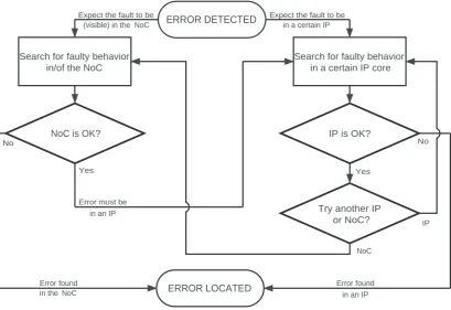
Networks-on-chip allow for communication-centric debug in addition to the traditional core-based debug. Communication-centric debug speeds up the localization of the IP core which causes the error and the point in time it occurs. A debug strategy for SoCs using NoCs is shown in Figure 3.3.
An error becomes visible at the IC pins, from where it must be traced back to the root cause. IC pins are either connected to an IP core or to the NoC. For each case there are two scenarios:
• An error is observed on an IC pin connected to the NoC. Examine all connections related to this pin and find out that either:
1. the NoC causes the error itself, or
application reset
program breakpoints
wait until breakpoint hit
reset chip
access registers
done
Figure 3.2: Traditional scan-based debug flow (Source: [31]).
• An error is observed on an IC pin connected to a certain IP core. Examine all connections with this IP core and find out that either:
3. the IP core causes the error itself, or
4. the IP core gets erroneous data from the NoC (find out whether it is scenario 1 or 2).
As can be seen the NoC will be examined first to determine whether it causes the error itself and if not which IP core does. Once the malfunctioning IP core (NoC included) is found it can be debugged with its built-in debug hardware (traditional core-based debug).
The big advantage of NoC is that it can raise the level of examination from bits to packets, messages or transactions. This makes it a lot easier to interpret what happens inside the IC. It also offers the possibility to compare it with a hardware-software co-simulation of the applica-tion, because at the lowest levels of software design abstracapplica-tion, also Transaction Level Models (TLMs) are used [33].
3.3
Debug Requirements for SoCs using NoCs
A recent paper [13] shows that it is possible to automatically insert monitors with the Æthereal design flow, covering 100% of the channels. Each monitor is connected to a router and can select one of its links at a time and has four abstraction levels, called analyzer modes. These modes are physical raw, logical connection-based, transaction-based and transaction event-based [14]. An Æthereal NoC with a NoC Monitoring Service (NoCMS), to be used for transaction level debug, has an average area overhead of 15% [13].
TN-2006-01234 Philips Restricted
ERROR DETECTED
ERROR LOCATED
NoC is OK? IP is OK?
Expect the fault to be (visible) in the NoC
Expect the fault to be in a certain IP
Error found in the NoC
Error found
in an IP
Search for faulty behavior in/of the NoC
Search for faulty behavior in a certain IP core
Try another IP or NoC?
Error must be
in an IP
NoC
No
Yes No
Yes
IP
Figure 3.3: Debug strategy for SoCs using NoCs.
in real-time compare connection data with a hardware-software co-simulation. However there are some restrictions which make the NoCMS not sufficient to completely rely on for debug of SoCs using NoCs. These restricitons are:
• Monitors are not suitbale for observing internal router and NI state information.
• Monitors must be programmed via the network, so they cannot be used for initialization problems or when the network or monitor configuration is broken.
• Monitors can only observe one link per router at a time.
• Monitors are not capable of sending raw link data real-time [14].
There are also some possibilities introduced by communication-centric design, which are not supported by monitors:
• NoC makes it possible to stop IP cores and the NoC itself on well defined points in time, by stopping on transactions instead of clock cycles.
• NoC can assist in IP core debugging by controlling the input data from the NoC.
3.3.1 Stop Operation
Traditional debug stops after a number of clock cycles or e.g. after a certain address has passed a number of times. NoC allows for stopping on transactions which has the following advantages:
• Both NoC and IP cores stop in a well defined state.
• It is easier for a debug engineer to determine where to stop using the software’s TLM.
• It is more robust in non-deterministic systems, where the point of time a transaction occurs can vary.
NoC separates all IP cores from each other and uses handshaking to communicate with them. By suppressing the valid and accept signals making up the handshake, the NoC will not accept data from IP cores or deliver data to IP cores. This stops the NoC functionally (i.e. it comes in some kind of idle mode, no data flow) so that its state can be dumped. The IP cores are still running in the meanwhile, with the exception that they cannot communicate with the network. After the NoC state is dumped, the valid and accept signal suppression can be removed and the application continues in a valid way.
Note that when only the clock of the NoC is stopped, the valid and accept signals keep their value. The consequence is that IP cores mistakenly assume that the NoC is producing valid data (when the valid signal was high) or it is accepting data (when the accept signal was high). This can result in loss of data coming from the IP cores and insertion of erroneous data into the IP cores. Therefore the above-mentioned method of supressing valid and accept signals at the border of the NoC is a prerequisite.
With the proposed stopping method, data in the NoC first ripples to the output buffers before it is functionally stopped. Clockgating can be applied in addition to stop the NoC more accurate.
3.3.2 Dump and Recover State
There are two possiblities to dump and recover the state of the NoC: (1) by scan chains (using IEEE 1149.1 also Joint Test Action Group (JTAG)) or (2) by using the network itself (e.g. by sending it to the Monitoring Service Access (MSA) point). The disadvantage of using scan chains is that it is slow, typically they are read out serially at 10 MHz. Advantages of scan chains are:
• It is a known technique.
• Scan chains must be inserted for test anyhow.
• Most IP cores use it already, so the TAP and infrastructure are already available.
• The JTAG port is also accessible when the IC is on an application board.
• It is supported by debugger tools.
• Not too much effort is needed to implement it.
TN-2006-01234 Philips Restricted
• There must be an instance that controls the emptying (and recovering) of the FIFO’s.
• The debugger tools must have an algorithm to be able to reconstruct the bits.
• Hardware must be added to lead the FIFO data back onto the network.
• For all remaining memory elements still a scan chain like solution is needed.
• What kind of output ports (64-bit, 32-bit etc.) should be supported?
So the only reason not to choose for scan chains would be if speed is really a bottleneck. An example will show if this is the case.
As an example we take the Nexperia TMPNX8525 chip, with 48 top-level design blocks [32]. To make an estimation of the time needed to scan out a NoC scan chain, we need to know the number of scannable elements in the NoC. Because FIFO’s in the NIs and routers dominate this number, only the number of channels is needed. Paper [13] discusses two real examples, a video and an audio application.
The video application has 15 processing cores and 42 channels. The audio application has 18 processing cores and 66 channels. We use this to estimate the number of channels needed when using NoC for the PNX8525:
(48 / (15 + 18)) * (42 + 66) = 157 channels.
Each channel contains a 32x32-bit FIFO at each NI (input and output buffer), whether BE or GT. Each router on the channel has a 3x34-bit FIFO for GT and a 24x34-bit FIFO for BE. Say half of the channels is BE, then (24x34 + 3x34) / 2 = 14x34 bits are on average per router in a channel. Using the different designs from [13], the router network needed for the NexperiaTM PNX8525 can be estimated on a 3x3 mesh, so say 3 routers on each channel. This makes the total average number of FIFO-bits per channel:
(32x32 x 2) + (14x34 x 3) = 3476 bits
With a debug clock of 10 MHz it would take (3476 x 157) / 10,000,000 = 0.05 s.
Even though only the FIFO’s were taken into account, from this example one can conclude that a lack of speed of scan chains is not an issue in the near-future.
3.3.3 Single Step and Continue Operation
Traditional single-stepping is applied at a clock cycle level. When in debug mode, one debug clock pulse steps the logic one cycle further (when shift enable is deactivated) [31]. This feature is very useful to observe where exactly an error occurs and is easily implemented with JTAG.
NoC introduces the possibility to step on more abstract levels, like flits, packets, messages and transactions. This can be done by reprogramming the breakpoints and then resume opera-tion. When a new breakpoint is hit the NoC will stop again and a new snapshot of the NoC state can be taken.
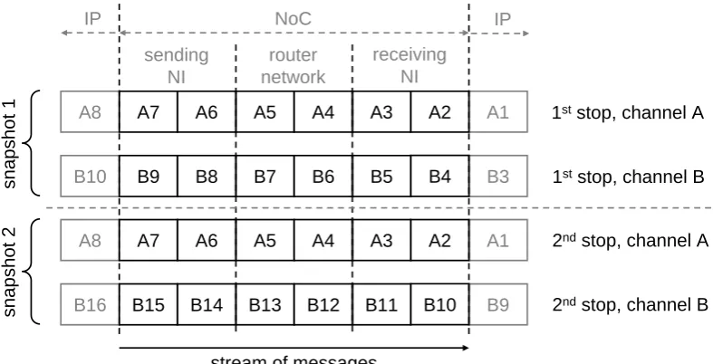
from 10 to 00). After the state recovery, the functional clock is put back and the IP cores can initiate and receive transactions again. It is also possible to let only a selective number of channels continue, see Figure 3.4. A variantion on this is to only release the valid and accept signals of the MNIP and not of the SNIP and vice versa. In this way only data is coming into the network or going out of the network.
A8 A7 A6 A5 A4 A3 A1
router network
receiving NI sending
NI
NoC
IP IP
1ststop, channel A
1ststop, channel B
2ndstop, channel A
B10 B9 B8 B7 B6 B5 B3
2ndstop, channel B
A8 A7 A6 A5 A4 A3 A1
B16 B15 B14 B13 B12 B11 B9
snapshot 1
snapshot 2
A2 A2
B4
B10
stream of messages
Section 4
Debug Architecture Design
This chapter starts with an overview of the design (4.1). Next the choices made to come to this design are treated (4.2). A new debug component, called stop module, is presented (4.3) and the last section discusses the core-based scan architecture (4.4).
4.1
Overview
Router 1 Network Interface kernel 2 Core 2 Port 2 BP-TPR Router 2 Core 1BP-TPR Port 1
Network Interface kernel 1
NoC
Monitor 2 Monitor 1 Stop Module 2 Delay Forced Stop TPR IP core Stop TPR Stop Module 1 Forced Stop TPR IP core Stop TPR Delay Clock Control TPR BP Gen TPR BP Gen TPR TAP Controller Breakpoint TPR OR-Gate OR-GateFigure 4.1: Overview of the debug architecture.
TN-2006-01234 Philips Restricted
The stop module is a component which takes care of the distribution of a breakpoint signal and is treated in section 4.3. The TAP controller can insert a breakpoint signal into the NoC just like the monitors. The delay insertion inside the NI is discussed in section 4.2.
All Test Point Registers (TPRs) are programmed (using scan) or read (only the breakpoint TPR) by the TAP controller. The breakpoint TPR is used to observe a breakpoint hit via JTAG. The BP Gen TPR is used to program the breakpoint hardware inside the monitor. The Forced Stop TPR indicates whether the message that is on its way must be finished or not when a breakpoint signal arrives. The IP Core TPR indicates whether the connected IP core clock must be stopped or not when a breakpoint signal arrives. The OR-gate combines the stop signal coming from the NoC with the one from the BreakPoint TPR (BP-TPR) of the IP core itself. The resulting signal goes to the Clock Control TPR (CC-TPR), which controls all clocks on the IC. This CC-TPR and the TAP controller are discussed in section 4.4.
4.2
Choices
4.2.1 Introduction
Based on the information of the previous chapter, the decision was made to stop the NoC by means of suppressing the valid and accept signals of the handshakes between NoC and IP cores. For dumping the state of the NoC scan chains are chosen.
The handshakes between NoC and IP cores take place on the NIPs as seen in Figure 2.6. On the NoC side these NIPs are connected to the protocol adapters in the NIs. In order to disrupt a handshake, the valid and accept signals going from the protocol adapter to the IP core must be deasserted. When the IP core wants to send/receive data but does not receive an accept/valid signal, there is no transfer.
To stop the whole NoC functionally, all protocol adapters must be aware of a breakpoint hit. The breakpoint signal must traverse the NoC to all NIs (which contain the protocol adapters). However, first the place of the breakpoint hardware must be determined.
Inside the monitors seems the perfect place for the breakpoint hardware, because they have 100% channel coverage [13] and can abstract link data on different levels (needed for transaction-based stopping and stepping).
4.2.2 Stop Signal Distribution
To get the breakpoint signal (also called stop signal, a pulse of one clock cycle on the stop wires) to the NIs there are two possibilities: centralized or distributed. A centralized unit sending the stop signal to all protocol adapters is not scalable and it is not obvious in a network which is distributed by nature. A dedicated interconnect is added for the stop events instead of using the network itself, because in the latter case the stop events might arrive too late at the NIs and the triggered event will be outside the NoC already.
The stop signal coming from the breakpoint hardware inside a monitor (either attached to a router or a NI) must be distributed to all NIs. One possibility is to put extra wires between neighbouring router and NI devices. Another possibility is to reuse the LLFC lines, as they are unused when the first and second word of a flit are sent. However extra wires have the following advantages compared to the latter option:
• The stop signal can be distributed three times as fast as a flit, because a flit needs three clock cycles to hop to another neighbour and the stop signal only one clock cycle. When using the LLFC wires this would be two times as fast, as the third cycle of a flit is used for LLFC itself.
• The monitor has one clock cycle more to generate the stop signal in worst case. This is because in worst case (shown in Figure 4.2) the stop signal cannot be sent in the third cycle of a flit when using the LLFC wires. With extra wires this is possible though.
In order to keep as much as possible unchanged of the current design, it is better not to add the extra wires between the routers and network interfaces. Instead, a separate network with the same topology as the router network is used to distribute the stop signal. The distribution is accomplished by stop modules positioned near all routers.
Although monitors can be attached to NIs it is assumed they are only attached to routers [13]. Figure 4.2 shows that this solution is feasible for even the worst case scenario. This is when is triggered on the 3rd word (W3) in a flit. To keep this within the NoC, the generation of the breakpoint may take 2 and a part of the third cycle, which must be sufficient. The part of the third cycle is because the stop module will be close to the monitor and not much time is needed to send over the stop signal.
clk
router_data_in
NI_kernel_data_in
W1 W2 W3
W1 W2 W3
W1 W2 W3
W1 W2 W3
protocol_adapter_data_in
IP_core_data_in
breakpoint generation time
stopmodule_stop_in
NI_kernel_stop_in
protocol_adapter_stop_in
1
2
3
4
5
6
7
8
9
Figure 4.2: Worst case breakpoint generation time. This is when a monitor needs to trigger on the last word of a flit (W3). Processing of the monitor can begin as soon as W3 arrives (cycle 4). As in worst case W3 (which must be kept inside the NoC) goes into the IP core in cycle 9, the stop signal must arrive at the protocol adapter in cycle 8 to be in time. Tracing back shows that the stop signal must be asserted by the monitor in cycle 6. This however, can be done at the end of this cycle because monitor and stop module will be close to each other in the floor plan. This results in a breakpoint processing time for the monitor of a little more than 2 clock cycles.
TN-2006-01234 Philips Restricted
4.2.3 Protocol Adapter
When the stop signal finally arrives at the protocol adapters, it depends on the Forced Stop TPR and the IP core Stop TPR what happens. The idea is to let messages finish which are on their way. In the protocol adapter it is easy to recognize when a message has ended, because then the statemachine returns to the initial state where it waits for a new message. As soon as the protocol adapter is in this state the valid and accept signals must be suppressed.
However it can take a while before all protocol adapters are in their initial state. There are two reasons why messages which are on their way can take a long time to finish: (1) the messages are big (e.g. when using MMBD) or (2) the supply of information by the initiating IP core is slow.
To be sure that the whole NoC is functionally stopped we use a second stop signal which is sent by JTAG. The 1st one can also be sent by JTAG, however this is of course far less accurate than the use of monitors, but can be helpful when something is wrong with them.
It is not possible to know when all transactions have finished because of the second of above-mentioned problems. Because this cannot be verified by the NoC either the second stop signal is sent when it can be reasonably assumed that most transactions are finished. This is up to the debug engineer.
The 2nd stop signal uses the same infrastructure as the 1st stop signal. Once the 2nd stop signal is received in the protocol adapters the valid and accept signals are suppressed, even when the transaction did not finish.
Because we use two stop signals we let receiving protocol adapters stop after the 1st stop signal when the transaction is finished. However, sending protocol adapters are only stopped at the 2nd stop signal. Thus data can get into the NoC but cannot go out of the NoC after the 1st stop signal and the transaction has finished. After the second stop signal data can neither go into or out of the NoC. After all data inside the NoC rippled to the other side, the NoC is functionally stopped.
The 2nd stop signal is called a forced stop signal, however the 1st stop signal can also be used as a forced stop signal depending on the value of the Forced Stop TPR. In this way the traffic on a channel can be frozen within a few clock cycles after the breakpoint hit.
Until now only the request channels were discussed, because there are no message headers in the response messages. In the future there will be, but now the signal rd_last is used, as seen in Figure 2.8. This signal indicates that the word on rd_data is the last word of a response message. The stopping of the response channel is done in the same way as the request channel.
The IP core Stop TPR is used to stop the clock of an IP core when there is a suspicion about an error in that IP core during a certain transaction (or other moment in time). As soon as the valid and accept signals are suppressed (which depends on the Force Stop TPR, how many stop signals are received and whether the transaction is finished) the signal going to the OR-gate will be asserted.
4.3
Stop Module
stop signal. This stop module is used everywhere, however signals not available at a certain place are connected to ’0’. This is easier to implement in the design flow at hand, than to generate a lot of different stop modules.
The jtag_stop, monitor_stop, stop_in and stop_out signals are considered as active-high pulses of one clock cycle. The breakpoint signal is active-high and stays active after the 1st stop signal is received (this signal is polled by JTAG). Reset is, just like all other reset signals in Æthereal, active-low. The clock signal is the same as the one from the NoC.
Master Stop Module clk
rst jtag_stop monitor_stop stop_in_0 stop_in_N
stop_out_0 stop_out_N
breakpoint
Figure 4.3: Master stop module with monitor stop signal, whereNis the number of neighbouring devices (routers and NIs).
There are a few requirements which must be satisfied by the stop modules:
1. All NIs must get both stop signals.
2. The distribution of the stop signal must behave like a wave in one direction (so the 1st stop signal can never be interpreted as the 2nd stop signal).
3. Only JTAG can initiate the 2nd stop signal.
4. Multiple breakpoints may hit in time and place, but may never cause a 2nd stop signal.
The conditions are:
1. Neighbouring stop modules are at a time distance of one clock cycle.
2. The JTAG stop signal is only attached to one stop module and used to inititate the 2nd and possibly the 1st stop signal.
3. Protocol adapters will not react on stop signals sent after the first two stop signals.
The statemachine shown in Figure 4.4 satisfies the above-mentioned requirements with respect to the conditions:
1. The statemachine only reacts in state 00 and 11 to an incoming stop signal.
2. Only after the transitions 00 -> 01 and 11 -> 00 a stop signal can be sent.
TN-2006-01234 Philips Restricted
00 01
11 10
!reset
jtag_stop OR stop_in !(jtag_stop OR stop_in)
!(monitor_stop OR jtag_stop OR stop_in) stop_out <= ‘0’
monitor_stop OR jtag_stop OR stop_in stop_out <= ‘1’
1
2 1
2
3
3
stop_out <= ‘0’
4 stop_out <= ‘1’
4 00 Wait for 1ststop signal. 01
10
11
Send a stop signal. Do nothing.
Wait for 2ndstop signal.
Figure 4.4: State machine of the stop modules, wherestop_inis the logical OR of allN neigh-bouring input stop signals andstop_outthe output signal going to allNneighbouring devices.
4. After the distribution of the 1st signal all stop modules end up in state 11. The second signal can only be initiated by JTAG because the stop modules are not sensitive to the monitors in state 11 (proof of requirement 3).
5. With multiple breakpoint signals in place and time, there are two ways waves can collide as shown in Figure 4.5. The waves either collide inside a stop module (a) or within two modules (b). In both cases the stop signal is only going into the direction(s) where it has not been (proof of requirement 2 and 4).
10 01 10
00
10 01 10
00
01
00
(a) (b)
6. The second stop signal, initiated by JTAG, is distributed almost in the same way as the 1st stop signal. However it causes a third stop wave too, before all stop modules end up in state 11 again (11 -> 00 is the second and 00 -> 01 is the third stop signal wave). This third stop signal is not a problem according to condition 3.
All this is visualized with a timing diagram in Figure 4.6 and an example in Figure 4.7.
clk
state 00 01 10 11 00 01 10 11
jtag_stop monitor_stop stop_in stop_out
Figure 4.6: Timing diagram of a stop module, depending on the stop module one of the gray signals per column is used. When in state 00, the signals jtag_stop, monitor_stop and stop_in are equivalent with respect to the behaviour of a stop module. The same counts for the signals jtag_stop and stop_in in state 11.
00 00 00 00 NI 0 NI 0 01 00 00 00 NI 0 NI 0 10 01 01 01 NI 1 NI 0 11 10 10 10 NI 1 NI 1 11 11 11 11 NI 1 NI 1 11 11 00 11 NI 1 NI 1 00 11 00 00 NI 1 NI 1 00 00 01 00 NI 2 NI 1 01 00 10 01 NI 2 NI 2 10 01 11 10 NI 3 NI 2 11 10 11 11 NI 3 NI 3 11 11 11 11 NI 3 NI 3 JTAG BP BP
1 2 3 4 5 6
7 8 9 10 11 12
TN-2006-01234 Philips Restricted
4.4
Core-based Scan Architecture
Figure 4.8 shows the core-based scan architecture used within Philips. Via de IEEE 1149.1 compliant TAP and the TAP controller test and debug of IP cores on an IC is done. Most cores have a BreakPoint Test Point Register (BC-TPR) which generates a breakpoint signal that goes to the Clock Control Test Pointer Register (CC-TPR). This CC-TPR is also shown in Figure 4.1 and can turn off the IP core clocks (or clock domains).
Each core has a Test Control Block (TCB) which is used for core isolation for manufacturing test. The Access Control Test Point Register (AC-TPR) is used for debug to select scan chains in the IP core to be scanned out via the output pin of the TAP.
clock generator
core 1 core 2 IEEE
1149.1 TAP
TAP controller
TCB TCB
TCB
CC-TPR
AC-TPR AC-TPR
BP-TPR BP-TPR
debug shell debug shell
test shell test shell
Section 5
Debug Architecture Implementation
This chapter starts with an overview of the implementation of the core-based scan architecture (5.1). Subsequently the implementation of the debug harware inside the clock control slice (5.2), the breakpoint hardware (5.3), the stop module (5.4) and the protocol adapter (5.5) is provided.
5.1
Overview
IP Stop TPR IP Stop TPR Force Stop TPR Force Stop TPR BP Hardware TPR BP Hardware TPR rdt_small_chip_bs_tb rdt_small_chip_bs rdt_small_chip TAP Controller tck trst_n tms tdi tdo tcb_enable tcb_update tcb_hold tcb_tdo tpr_enable tpr_update tpr_capture tpr_hold tpr_tdo Traffic Generators rdt_small_core TCB CCS jtag_stop dbg_clock_req dbg_so tdi tck tpr_bypass tpr_config tpr_se dbg_stop_req tcb_clock_mode rdt_small_network [1..0] Reset GeneratorClock Generator clk_func_in clk_func_out rst_n Breakpoint TPR Stop Module break_point Force Stop TPR IP Stop TPR BP Hardware TPR
Figure 5.1: Overview of the implementation of the core-based scan architecture.
TN-2006-01234 Philips Restricted
(small is the name of the example used). The clock and reset generators as well as the traffic generators are placed at the chip level. This, because later on the traffic generators will be replaced by real IP cores, which should be on chip level.
The TAP controller, TCB and TPRs are created with a Philips tool called TimNet after configuring TimNet files. The Clock Control Slice (CCS) is used to switch between functional and debug clock and its implementation details are given in section 5.2.
5.2
Clock Control Slice
After the NoC is functionally stopped, the functional clock must be switched off. Next, the shift enable (also scan enable) signal is asserted and then the debug clock is applied to the NoC to start shifting out the NoC state. Figure 5.2 shows the implementation of the CCS, which is a simple version of the one described in [31]. Figure 5.3 shows the timing diagram belonging to this CCS. In Appendix A the VHDL code is given.
clk_func_in
rst_n tck
clk_test dbg_clock_req
dbg_stop_req tcb_clock_mode[1..0]
func_clk_out 1
0 1
0 rdt_debug_ccs
Figure 5.2: Clock control slice (Source: [31]).
5.3
Breakpoint Hardware
The monitor discussed in [13] has been partially implemented [16]. However there were some problems synthesizing it. As for this project only very basic programmable breakpoint hardware was needed, the decision was made not to use it. Instead, the breakpoint hardware shown in Figure 5.4 has been implemented.
tcb_clock_mode[1]
tcb_clock_mode[0]
dbg_stop_req
clk_func_in
clk_func_out tck dbg_clock_req
Reprogramming the TCB
tcb_clock_mode[1]
dbg_stop_req
clk_func_in
clk_func_out tck dbg_clock_req
Figure 5.3: Timing diagram of the control clock slice (Source: [31]).
5.4
Stop Module
The VHDL code of the stop module is given in Appendix C. This consists of the state machine of Figure 4.4, an edge detector for the slow JTAG stop signal and some logic to keep the breakpoint signal high. The latter is needed because if there would be a breakpoint hit at the moment the status of the breakpoint TPR is captured, it will be missed. The logic in Figure 5.5 (a) will keep the signal high once there is a breakpoint hit.
It must be possible to send the 1st stop signal with JTAG (instead of a monitor). However the debug clock is much slower than the functional clock and thus the jtag_stop signal will be high for many functional clocks. Normally the signal would then also be used as an unwanted 2nd stop signal. The active edge detector in Figure 5.5 (b) makes a pulse of this signal.
5.5
Protocol Adapter
TN-2006-01234 Philips Restricted
clk rst_n
rdt_debug_breakpoint_gen
link_data[33..32]
monitor_config[32]
monitor_stop
counter
flit validity check
link_data[31..0]
monitor_config[31..0]
word_count
data comparison valid_flit
Figure 5.4: Simple breakpoint hardware. Monitor_config is attached to a TPR; with bit 32 the breakpoint hardware can be enabled and bit 0-31 are used to compare with bit 0-31 of link_data. Bit 32 and 33 of link_data are the sideband bits and are together with a counter used to determine the validity of a flit. The monitor_stop signal goes to a stop module.
break_point_nxt
stop_nxt break_point
jtag_stop_aed jtag_stop_dly
jtag_stop
(a) (b)
clk stop_nxt break_point
clk jtag_stop jtag_stop_aed
NoC clock NoC clock
Section 6
Results
The presented debug architecture has been fully integrated in the Æthereal design flow (the changes are presented in Appendix E). That is, it is generated for any topology of the network and can be switched on with DEBUG_HARDWARE = YES (default: NO) in the makefile of the example. Another variable in the makefile is JTAG_STOP = RXX, which indicates that the stop module near router RXXis the master stop module and connected to the TAP controller (default: R00).
A debug library (rdt_debug_lib) has been added which contains all debug related modules, such as the TPRs, the stop modules, the TCB, the CCS, the breakpoint hardware and a BFM-writer. The latter is used to simulate stimuli generated by the debug program Incide. Three scipts are written for Incide (incide.sh): (1) Incide determines the length of the connected scan chain, (2) Incide generates stimuli which can be simulated with help of the BFM-writer and (3) Incide is connected to the design, programs a breakpoint, wait till a hit and dumps the NoC state.
How this all works is indicated in Appendix F. This "getting started" manual explains exactly which steps must be taken. Basically first a NoC is generated; this is synthesized, next scan chains are inserted and finally the debug program Incide can be connected to it.
With the second Incide script (see Appendix F) stimuli are generated to program a breakpoint and send the JTAG stop signal. Figure 6.1 shows the simulation of the breakpoint hit and the 2nd stop signal inititated by JTAG, for the master stop module.
With the third Incide script a statedump is made after a breakpoint hit is detected and the JTAG signal is sent. The bits that shifted out of the design can subsequently be reconstructed to their Register Transfer Level (RTL) equivalents (see Appendix F). Figure 6.2 shows the recon-struction for the memory elements in the stop modules. The states (state_r) are hexadecimal 3, so binary 11 as they were expected to be. Also the breakpoint signal (break_point_r_reg) is as expected active (’1’). Figure 6.3 shows two statedumps made with different breakpoints. The time distance between both statedumps is two packets and not like in traditional debug one clock cycle.
TN-2006-01234 Philips Restricted
Figure 6.1: The master stop module receives a stop signal from two neighbours at the same time. Next clock cycle it makes the breakpoint signal active and sends a stop signal to all its neighbours. After a certain time (which is made short now for the overview) JTAG stop is asserted and the second stop signal wave (and consequently a third) is initiated.
by the efficient ones. Eventually it is assumed to be around 4% of the NoC area. This number contains all added hardware inside the NoC core, see Figure 4.1.
TN-2006-01234 Philips Restricted
Section 7
Conclusions and Future Work
This chapter draws conclusions (7.1) and points out what still needs to be done (7.2).
7.1
Conclusions
Networks-on-Chip emerge as the new type of interconnect for next-generation systems-on-chip. They overcome the upcoming deep sub-micron effects, the increasing design complexity and the lack of scalability of busses. However NoCs can also assist in SoC debug as this report shows.
Looking at the communication of SoCs might help the debugging proces of prototype ICs. Raising the abstraction level from bits to transactions makes it easier to interpret and compare what happens inside the NoC with a software transaction level model.
The proposed debug architecture and strategy may speed up the localization of erroneous IP cores and timing errors. Subsequently, the malfunctioning IP core can be stopped at the right moment using the added breakpoint hardware in the NoC. Using the IP cores’ debug facilities and the controlled data supply from the NoC side, the error might be found more quickly.
The proposed communication-centric debug solution assists in both NoC and SoC debug. It has been fully integrated in the Æthereal design flow and increases the NoC area with around 4%. To determine whether it really decreases the debug-time-to-root-cause it must be tested on e.g. an Field Programmable Gate Array (FPGA). However some things need to be improved and added first as discussed in next section.
7.2
Future Work
In order to be able to use the proposed communication-centric debug solution, a number of things need to be done:
• Add an AC-TPR debug shell to support multiple scan-chains.
• Add more advanced breakpoint hardware and integrate it with the debug/performance monitors.
• Adjust the debugger tools to support easy breakpoint programming, state dumping and stepping.
TN-2006-01234 Philips Restricted
References
[1] William J. Dally and Brian Towles. Route Packets, Not Wires: On-Chip Interconnection Networks. InProc. of the 38th Design Automation Conference (DAC), June 2001.
[2] Giovanni De Micheli and Luca Benini. Networks on Chip: A New Paradigm for Systems on Chip Design. InProc. of the Design, Automation and Test in Europe Conference and Exhibition (DATE), pages 418–419, Washington, DC, USA, 2002. IEEE Computer Society.
[3] Paul Wielage and Kees Goossens. Networks on Silicon: Blessing or Nightmare? InProc. of the EUROMICRO Symposium on Digital System Design (DSD), Dortmund, Germany, September 2002.
[4] Jörg Henkel, Wayne Wolf, and Srimat T. Chakradhar. On-chip networks: A scalable, communication-centric embedded system design paradigm. InProc. of the 17th Interna-tional Conference on VLSI Design (VLSID), pages 845–851, 2004.
[5] Kees Goossens. Networks on Chip for Consumer Electronics. InProc. Int’l Summer School on Advanced Computer Architecture and Compilation for Embedded Systems (ACACES), pages 227–230, July 2005.
[6] A. Hemani, A. Jantsch, S. Kumar, A. Postula, J. Öberg, M. Millberg, and D. Lindqvist. Network on chip: An architecture for billion transistor era. InProc. of the IEEE NorChip Conference, November 2000.
[7] Axel Jantsch and Hannu Tenhunen, editors.Networks on chip. Kluwer Academic Publish-ers, 2003.
[8] Robert D. Mullins. An On-Chip Network Bibliography, 2006.
[9] Arteris. A Comparison of Network-on-Chip and Busses, February 2005.
[10] William Orme. Debug IP for SoC Debug, December 2005.
[11] DAFCA. DAFCA In-Silicon Debug: A Practical Example, June 2005.
[12] Bart Vermeulen, Tom Waayers, and Sandeep Kumar Goel. Core-Based Scan Architecture for Silicon Debug. InITC, pages 638–647, 2002.
TN-2006-01234 Philips Restricted
[14] C˘alin Ciorda¸s, Kees Goossens, Twan Basten, Andrei R˘adulescu, and Andre Boon. Trans-action Monitoring in Networks on Chip: The On-Chip Run-Time Perspective. InProc. of the IEEE Symposium on Industrial Embedded Systems (IES), October 2006.
[15] C˘alin Ciorda¸s, Kees Goossens, Andrei R˘adulescu, Kees Goossens, and Twan Basten. NoC Monitoring: Impact on the Design Flow. InProc. Int’l Symposium on Circuits and Systems (ISCAS), May 2006.
[16] Andre G. Boon. The hardware design of Monitoring Probes for the Æthereal NoC, January 2006.
[17] C˘alin Ciorda¸s, Basten, Twan, Andrei R˘adulescu, Kees Goossens, and Jef van Meerbergen. An Event-Based Network-on-Chip Monitoring Service. InProc. of the High-Level Design Validation and Test Workshop (HLDVT), pages 149–154, November 2004.
[18] Bart Vermeulen, John Dielissen, Kees Goossens, and C˘alin Ciorda¸s. Bringing Commu-nication Networks On Chip: Test and Verification Implications. IEEE Communications Magazine, 41(9):74–81, September 2003.
[19] Axel Jantsch and Hannu Tenhunen. Will Networks on Chip Close the Productivity Gap? InNetworks on Chip, chapter 1, pages 3–18. Kluwer Academic Publishers, February 2003.
[20] E. Bolotin, I. Cidon, R. Ginosar, and A. Kolodny. Cost Considerations in Network on Chip. Integration - The VLSI Journal, Special issue: Networks on chip and reconfigurable fabrics, 38, Issue 1:19–42, October 2004.
[21] Andrei R˘adulescu and Kees Goossens. Æthereal Services, July 2003.
[22] Kees Goossens, John Dielissen, and Andrei R˘adulescu. The Æthereal Network on Chip: Concepts, Architectures, and Implementations. IEEE Design and Test of Computers, 22(5):414–421, September-October 2005.
[23] John Dielissen, Andrei R˘adulescu, Kees Goossens, and Edwin Rijpkema. Concepts and Implementation of the Philips Network-on-Chip. In IP-Based SOC Design, November 2003.
[24] Kees Goossens, John Dielissen, Om Prakash Gangwal, Santiago González Pestana, Andrei R˘adulescu, and Edwin Rijpkema. A Design Flow for Application-Specific Networks on Chip with Guaranteed Performance to Accelerate SOC Design and Verification. InProc. of the Design, Automation and Test in Europe Conference and Exhibition (DATE), pages 1182–1187, March 2005.
[25] Razvan Dinu. Analysis and Refactoring of a Design Flow for Application-Specific Net-works on Chip, August 2005.
[26] Andrei R˘adulescu, John Dielissen, Santiago González Pestana, Om Prakash Gangwal, Ed-win Rijpkema, Paul Wielage, and Kees Goossens. An Efficient On-Chip Network Interface Offering Guaranteed Services, Shared-Memory Abstraction, and Flexible Network Pro-gramming. IEEE Transactions on CAD of Integrated Circuits and Systems, 24(1):4–17, January 2005.
[28] OCP International Partnership. Open Core Protocol Specification. Version 2.0, September 2003.
[29] ARM Limited. AMBA AXI Protocol Specification. Version 1.0, March 2004.
[30] K. Goossens, J. van Meerbergen, A. Peeters, and P. Wielage. Networks on Silicon: Com-bining Best-Effort and Guaranteed Services. InProc. of the Design, Automation and Test in Europe Conference and Exhibition (DATE), pages 423–425, March 2002.
[31] Philips Semiconductors. CoReUse 4.1: Core-based Scan Architecture for Silicon Debug. Version 1.4, February 2003.
[32] Bart Vermeulen, Steven Oostdijk, and Frank Bouwman. Test and debug strategy of the PNX8525 NexperiaTMdigital video platform system chip. InITC, pages 121–130, 2001.
Appendix A
Clock Control Slice Implementation
ARCHITECTURE rtl OF rdt_debug_ccs IS SIGNAL clk_func_in_not : std_logic;
SIGNAL dbg_stop_req_1, dbg_stop_req_2, dbg_stop_req_2_not : std_logic; SIGNAL mux0_0, mux0_1, mux1_0, mux1_1 : std_logic;
BEGIN
mux0_0 <= clk_test;
mux0_1 <= dbg_clock_req AND tck; PROCESS(mux0_0, mux0_1, tcb_clock_mode) BEGIN
IF (tcb_clock_mode(1) = ’1’) THEN mux1_1 <= mux0_1;
ELSE
mux1_1 <= mux0_0; END IF;
END PROCESS;
PROCESS(clk_func_in) BEGIN
IF (clk_func_in’EVENT AND clk_func_in = ’1’) THEN IF (rst_n = ’0’) THEN
dbg_stop_req_1 <= ’0’; ELSE
dbg_stop_req_1 <= dbg_stop_req; END IF;
END IF; END PROCESS;
clk_func_in_not <= NOT clk_func_in; PROCESS(clk_func_in_not)
BEGIN
IF (clk_func_in_not’EVENT AND clk_func_in_not = ’1’) THEN IF (rst_n = ’0’) THEN
dbg_stop_req_2 <= ’0’; ELSE
dbg_stop_req_2 <= dbg_stop_req_1; END IF;
END IF; END PROCESS;
dbg_stop_req_2_not <= NOT dbg_stop_req_2; mux1_0 <= clk_func_in AND dbg_stop_req_2_not; PROCESS(mux1_0, mux1_1, tcb_clock_mode) BEGIN
IF (tcb_clock_mode(0) = ’1’) THEN clk_func_out <= mux1_1;
ELSE
clk_func_out <= mux1_0; END IF;
Appendix B
Breakpoint Hardware Implementation
ARCHITECTURE rtl OF rdt_debug_breakpoint_gen IS SIGNAL state_r, state_nxt: natural range 0 to 2; SIGNAL filled_flit_r, filled_flit_nxt : std_logic; SIGNAL link_data_r : std_logic_vector(33 downto 0); BEGIN
state: PROCESS(clk) BEGIN
IF RISING_EDGE(clk) THEN IF (rst_n = ’0’) THEN
state_r <= 2;
filled_flit_r <= ’0’;
link_data_r <= (OTHERS => ’0’); ELSE
state_r <= state_nxt;
filled_flit_r <= filled_flit_nxt; link_data_r <= link_data;
END IF; END IF;
END PROCESS state; cnt: PROCESS(state_r) BEGIN
IF state_r = 2 THEN state_nxt <= 0; ELSE
state_nxt <= state_r+1; END IF;
END PROCESS cnt;
ff: PROCESS(filled_flit_r, state_r, link_data_r) VARIABLE var_filled_flit: std_logic;
BEGIN
![Figure 2: Example DTL ConnectionsFigure 2.8: DTL signals (Source: [27]).](https://thumb-us.123doks.com/thumbv2/123dok_us/1165792.1146709/18.595.97.512.190.597/figure-example-dtl-connectionsfigure-dtl-signals-source.webp)
![Figure 3.1: Digital design flow (Source: [31]).](https://thumb-us.123doks.com/thumbv2/123dok_us/1165792.1146709/19.595.87.498.386.648/figure-digital-design-ow-source.webp)
![Figure 3.2: Traditional scan-based debug flow (Source: [31]).](https://thumb-us.123doks.com/thumbv2/123dok_us/1165792.1146709/21.595.223.360.86.329/figure-traditional-scan-based-debug-ow-source.webp)