An Analysis of Multipliers in a New Binary
System
R.K. Dubey & Anamika Pathak
Department of Electronics and Communication Engineering , Swami Vivekanand University,
Sagar (M.P.) India 470228
Abstract:Bit-sequential multiplier is being studied in a (+1, -1) binary representation. The maximum length of multiplier for a fix point numbers consists of n module. Each module is a five bit adder which contains 5 inputs and 3 outputs. It also contains an additional pin at the input as well as at the output. Computation time for multiplication is of the order of O(n). Hardware realization of module is being discussed. In this design the input generated bit sequentially and the output is also generated bit sequentially. The model is being compared with the bit sequential multiplier in conventional binary system and the merits and demerits are described in detail.
Index Terms: Add-shift multiplier, (+1, -1) Representation, Carry-save addition, unified way.
1. INTRODUCTION:
In digital signal processing design of fast efficient multipliers is currently an interesting area of research. Multipliers have been extensively studied by various authors [1-5] for VLSI design. Many scientific and engineering problems, such as inversion of materials, solution of line or equation, computation of eigen value, Fast Fourier Transform and Discrete Fourier Transform and modular arithmetic etc. require large number of multiplications. For computer hardware designers, it is most important to know current research concerning the multiplier for LSI technology.
The conventional add-shift technique of multiplication take time O(n2) with n being the maximum lengths of multiplier and multiplicand. This time can be reduced to O(nlog-n) using carry look ahead technique for addition but it complicates the hardware design.
Bit serial arithmetic is often used in parallel systems with high connectivity to reduce the wiring to a reasonable level. When multiplication is required, a serial-parallel multiplier is a typical choice but this scheme is not always possible. When both the inputs are required to enter serially at the same time then serial multiplier is required. Bit serial input and output multipliers referred to as on line multipliers [1] are potentially attractive in speeding up the execution of arithmetic expression, where multiprocessor arithmetic structure is needed. Bit serial input and output multiplier was presented by Lyon [2]. Full precision modular serial multipliers for unsigned numbers were introduced by Sips
[3] and Strader and Ryne [6]. Gnanasekaran and Sunar [7, 18] presented a bit serial input and bit serial output multiplier for unsigned and two's complement numbers. It directly takes into account the negative weight most significant digit in two's complement representation. Chen & Willoner and Hasan [8, 17] presented O (n) parallel multiplier with bit-sequential input and output. This multiplier for n bit operands requires 2n clocks and 2n number of 5 input modules.
L. Dudda (9) discussed the serial multipliers for two's complement numbers. The multiplier includes a linear array of (5, 3) parallel counters and a set of three static registers for internal carries. He showed that equivalent multiplier can be built using two linear arranges of full adders and two carry registers. In a faster circuit an addition carry register is required. Bit-serial multipliers and squares is presented for signed and unsigned numbers by Inne and Viredaz [10]. It produces a full precision result which can be extended to an arbitrarily large number. It is fully modular and it has zero clock cycle latency. It has got one disadvantage that last sub product most be subtracted keeping only first k bits. Large number extra bits are required for sign. It results in over complicated design which requires the knowledge of the cycle when the sign bit is presented.
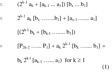
In digital signal processing, the number representation (+1, -1) is found suitable as discussed by author [11]. It is a unified representation of positive as well as negative numbers. Full addition, filter design, D/A and A/D conversion is being discussed there in detail. The flip-flops, adders and comparators in this system is described in detail by Tiwari and Varma [12, 13]. In this paper our main aim is to study bit serial multipliers in (+1, -1) system. The method of multiplication is based on add-shift-technique where multiplication bits and multiplier bits are entered sequentially. A module of 5 bit adders is employed. The positive and negative numbers are multiplied in a unified manner. Additional bits are required to modify the effect of -1 bit in place of 0 bit. For fast addition, carry save addition is employed.
II. BIT SEQUENTIAL MULTIPLIER
Following [7] serial multiplier operation for positive and negative members in (+1, -1) representation can be constructed in the following way.
can be accomplished by carry save adders in which the carry generated as each stage is saved and propagated only to the adjacent stage in the next addition. At each stage, the second and third terms shifted one bit left then added to 1st term. The right most bit of 1st term is not involved in addition process and is already available as output. Thus during the whole multiplication process maximum number of adders required is equivalent to the total number of multiplier bits. In equation (1), ak and bk can take the values
as ak = +1, bk = +1, ak = -1, bk= -1, ak= -1, bk = +1 and
ak = +1, bk =-1. Thus the product bit akbk is either positive
(+1) or negative (-1).
As an illustration, the step by step multiplication process according as eqn. (1) for four bit positive as well as negative operand is shown in fig. 1. For a carry save addition P-digits in 1st term is in redundant binary form. In the 1st step, the multiplied bit is a1 b1 which is the 1st term
of eqn. (1) and remaining two bits will be -1 and + 1 or + 1 and -1 depending on product from A carry bit + 1 or -1 is generated which will be saved and added to the next step. The sum bit is represented as P1. During second cycle or
step, the product bits will be a2 b1, a2b2 and b2a1 and they
are added to the sum bit P1 after shifting one bit left. The
sum bit P2 contains the product bits a2b1 and b2a1 and bit –1
or
1
since1
produces an error during addition, so the error is removed by adding an extra bit +1. It also contains the carry bit from the previous stage. Thus, there will be total 5 bits for addition. The addition of 5 bits produces a sum bit P2 and two bits carry for the next step. The sum bitP3 contains the product bit a2 b2 and bits
1
and1
. The bits1
and1
are error bits and can be eliminated by adding two extra bits +1 and +1. Thus, the sum of 5 bits (1
,1
a2b2, 1 1), will produce P3 and two bits for carry to the next
step.
For step-3, we have the product bits a3b3, a3b2, a3b1, b3a2
and b3a1. These bits are shifted one bit left and added to
previous sum with saved carry bits. During addition the previous sum P2, P1 become free but P3 is added to a3 b1
and b3a1 two bits of previous carry. Thus there will be total
5 bits. The sum of these bits produce the sum bit P3 and two
bits for carry for the next step. The sun bit P4 contains a3b2
and b3a2 -1 and two carry bits from the 2nd step. The bit,
1
produce an error which is over come by taking into consideration an extra bit of opposite nature i.e. + 1. Thus, there will be total six digit for sum. The addition of two bits
discussed in step-3. Finally, we find that P1, P2, P3 are free
bits and they do not take part in addition. Four 5 bit adders are required for whole multiplication process. Fig. (2) points out the specific example for four bit numbers A =
1
1
11
= - 11 and B = 11
1
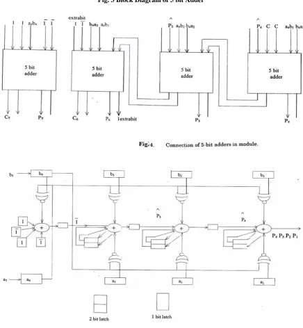
1 = 3 multiplication in four steps.Hardware realization of five bit adders is shown in figure (3). It consists two product bits A and B for a particular step one previous sum bit and two bits for carry from previous step as inputs; two bits for carry and one bit for sum as outputs. 4 bit serial multiplier for 4th clock cycle connection of module is shown in Fig. (4). The third module of adder produces a "two bit" sum where one bit of the sum is extra bit to make the result error free because an error bit + 1 exists in the input. This extra bits is +1. Thus the sum bit contains an additional bit +1. Fourth adders contain fixed bits
1
,1
, 1, 1 and one product bit a4b4. Thesum bit is always the product bit. Hardware realisation of a four bit serial multiplier during 4th clock interval is shown in Fig. (5).
Fig. 3 Block Diagram of 5 bit Adder
instead of AND gate. The queue register implementation requires additional hardware a switch and tristate inverter. Positive as well as negative numbers are multiplied with the same type hardware. In this way, the hardware realization of multiplier is straight and simple. The main advantage of this system is the unified implementation of positive as well as negative numbers. The two's complement multipliers are realized in different manners, as discussed by authors [8-10] compared to positive numbers. Our model is well suited for digital signal processing where parallel processing for positive and negative number are required simultaneously. A multiplier cell can be constructed and connected in modules, which helps in LSI design. The draw back of this system is that it is partially suitable for computation because even numbers can not be generated.
REFERENCES:
(1) K.S. Trivedi and M.D. Ercegovae, "On line algorithms for division and multiplication", IEEE Trans. Comput. Vol. C-26, pp 681-687. July 1977.
(2) R.F. Lyon, "Two's Complement pipe line multipliers", Vol. COM-24, no. 4 pp. 418-425, Apr. 1976.
(3) H.J. Sips, "Comments on 'An O(n) parallel multiplier with bit sequential input and output", IEEE Trans. Compo. Vol C-31, no. 4, pp. 325-327 Apr. 1982.
10.Oct. 1979.
(9) L. Dadda "On serial input multiplies for two's complement numbers" IEEE Trans. Comput. Vol. 38, No.9, pp 1341-1345, Sept. 1989. (10) P. Ienne and M.A. Viredaz, "Bit Serial multipliers and squares",
IEEE Trans. Comput. Vol. 43, no. 12 December, 1994.
(11) K.Z. Pekmestzi, "New number representation for digital signal processing", Int. J. Electronics, Vol. 66, No.5, pp. 709-723, 1989. (12) M. Tiwari and H.V. Varma, "Logical design of adders and
Comparators", Indian Journal of Technology; Vol. 31, pp. 126-130, March, 1993.
(13) M. Tiwari and R.V. Varma. "Flip-flops in a new binary system, Indian Journal of Engineering and Materials Sciences, Vol. 2, pp. 8-11 Feb. 1995.
(14) A. Reyhani- Masolrh, “ Low complexity word level sequential normal basis multiplier” IEEE Transaction on Computers-2005 (15) Y. Chang, T. K. Truong, I. S. Reed, et. Al., “Algebraic decoding
of(71,36,11),
(79, 40, 15), and (97, 49, 15) quadratic residue codes,” IEEE Trans. Comm., vol. 51, pp. 1463-1473, 2003.
[16] A. Reyhani-Masoleh and M. A. Hasan. “Efficient Digit-Serial Normal Basis Multipliers over GF (2M)”. In IEEE International
Symposium on Circuits and Systems, ISCAS 2002, pages 781–784, May 2002.
[17] A. Reyhani-Masoleh and M. A. Hasan. “Efficient Multiplication beyond Optimal Normal Bases”. to appear in IEEE Transactions on Computers, Special Issue on Cryptographic Hardware and Embedded Systems, April 2003.