IJEDR1503056 International Journal of Engineering Development and Research (www.ijedr.org) 1
Reduction of Leakage Power in CMOS circuits
(Gates) using Variable Body Biasing with sleep
insertion Technique
1Sunita Yadav, 2Vishal Ramola
1M.Tech. Student of VLSI Design Department, UTU Dehradun, UK India 2Assist. Prof. VLSI Design Department, UTU, Dehradun, UK India2
________________________________________________________________________________________________________
Abstract - Leakage Power is the major problem in digital circuits. There are various techniques to reduce the leakage power technique. One technique discussed in this paper. We propose a technique called Variable body biasing for designing logic gates which significantly cuts down the leakage current without increasing the dynamic power dissipation, sleep insertion technique is also added along with variable body biasing technique so that there is no loss of state as in sleep stack technique. This thesis proposed a technique that reduces both power dissipation and glitches. This technique is based on two methods first is variable body biasing and the other is sleep insertion technique. Pass transistor is also added in the circuitry in order to eliminate glitches if any. The existing leakage reduction techniques like sleepy keeper and stack technique are having drawbacks like increased area and delay. Other delay elements that are used for reduction in glitches takes larger area when compared with pass transistor. This new proposed approach eliminates leakage power along with glitches keeping in mind all the drawbacks of all the earlier techniques. All the performance has been investigated using 90nm Technology at 1 voltage and evaluated by the comparison of the simulation result obtain from TSPICE.
Keywords - VBBT, Delay, leakage power, sleep insertion technique
________________________________________________________________________________________________________
I. INTRODUCTION
The development of digital integrated circuits is challenged by higher power consumption. The combination of higher clock speeds, greater functional integration, and smaller process geometries has contributed to significant growth in power density. Scaling improves transistor density and functionality on a chip. Scaling helps to increase speed and frequency of operation and hence higher performance. As voltages scale downward with the geometries threshold voltages must also decrease to gain the performance advantages of the new technology, but leakage current increases exponentially. Thinner gate oxides have led to an increase in gate leakage current.
Today leakage power has become an increasingly important issue in processor hardware and software design. With the main component of leakage, the sub-threshold current, exponentially increasing with decreasing device dimensions, leakage commands an ever increasing share in the processor power consumption.
Static power refers to the power dissipation which results from the current leakage produced by CMOS transistor parasitic. Traditionally static power has been overshadowed by dynamic power consumption, but as transistor sizes continue to shrink, static power may overtake dynamic power consumption To alleviate the rising significance of static power in digital systems, static power reduction technique shave been developed like transistor stacking, dual threshold voltage , MTCMOS etc. Some of these techniques are state saving and some are state destructive techniques. For example: Sleep transistor is a state destructive technique. Despite the rising significance of static power in CMOS circuits, the dynamic power is still the major contributor to power consumption. Dynamic power is mostly consumed by glitches which are the unwanted transitions and need to be eliminated. Glitch and leakage power both are the main contributors to the power consumption and needs to be reduced.
However, low-power design usually involves making tradeoffs such as timing versus power and area versus power. Increasing performance, while the power dissipation is kept constant, is also considered to be a low-power design problem. In fact, higher performance-per-watt is the new technique for micro-processor chip manufacturers today. In order to achieve high density and high performance, CMOS technology feature size and threshold voltage have been scaling down for decades. Because of this trend, transistor leakage power has increased exponentially. The reduction of the supply voltage is dictated by the need to maintain the electric field constant on the ever shrinking gate oxide.
The paper is organized as follows: in Section II, previous work is reviewed. Subsequently, in section III, the modified Low power logic gates with VBBT approach are presented. In section IV, the simulation results are given and discussed. The comparison and evaluation for modified and existing designs are carried out. Finally a conclusion will be made in the last section.
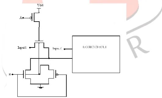
II. PRELIMINARIES A. Sleep Mode Approach
© 2015 IJEDR | Volume 3, Issue 3 | ISSN: 2321-9939
IJEDR1503056 International Journal of Engineering Development and Research (www.ijedr.org) 2 and reduces the leakage current[13]. During active mode we ON the sleep transistor and direct connection of circuit with Vdd, so increase the performance of the circuit and Reduces the leakage power efficiently.
Figure 1 Sleep Approach NAND gate
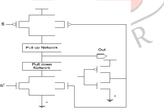
B. Leakage Feedback Approach
Another Leakage reduction technique is leakage feedback approach; In this approach we use two parallel PMOS transistor above pull up network and Vdd [6]. To provide the inverting output of the circuit we connect inverter at the output, an inverter provides the proper logic feedback to both pull down NMOS(S') and pull up PMOS(S) sleep transistor as shown in Fig.2. This two transistor enhance the circuit performance and maintain the proper logic of the circuit during standby mode. In standby mode one of the transistor of parallel sleep transistor turn off both NMOS and PMOS, the output of the circuit is pass through inverter which keep ON one of the sleep transistor which is connected parallel by providing the proper feedback approach. Hence circuit is active in standby mode, we mitigate the various leakage current which flow during standby mode and increase the performance of the circuit.
Figure 2 Leakage Feedback Approach
C. Sleepy Keeper Approach
IJEDR1503056 International Journal of Engineering Development and Research (www.ijedr.org) 3 Figure 3 Sleepy keeper Approach based 2 input NAND gate
D. Proposed VBBT with Sleep insertion technique
This new sleep variable body biasing technique reduces both leakage power and glitch in the logic circuit. This design includes both-
(i)Variable body biasing and (ii)Sleep insertion technique
Sleep insertion technique is a state destructive technique that cuts off either pull-up or pull-down or both the networks from the supply voltage or ground or both using sleep transistors. This technique is an extension to MTCMOS, which adds downnetworks and ground while for fast switching speeds, low-vth transistors are used in logic circuits, this process reduces leakage power during sleep mode.
The source of one of the sleep transistor is connected to the body of other sleep transistor in order to have a variable body biasing effect. Due to this connection the threshold voltage of the sleep transistors increases due to variable body biasing during sleep mode.
Figure 4 Variable Body Biasing with Sleep Insertion Technique
III. APPLYING VBBT ALONG WITH SLEEP INSERTION TECHNIQUE TO CMOSCIRCUITS
Various circuit applications of the VBBT technique are explored in this section. The VBBT technique with sleep insertion technique is applied to the following CMOS circuits and also the irrespective base case are implemented to calculate the amount of leakage power reduced in VBBT technique.
© 2015 IJEDR | Volume 3, Issue 3 | ISSN: 2321-9939
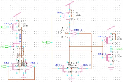
IJEDR1503056 International Journal of Engineering Development and Research (www.ijedr.org) 4 Figure 5 Schematic diagram of AND gate with variable body biasing
The VBBT based AND gate is shown in Figure5 with the two transistors used as variable body biasing and one transistor is added in order to add stack approach so that the disadvantage of state destructive stage is overcome. The simulation waveforms of VBBT AND gate from Figure4 show that the basic characteristics of AND are retained by VBBT AND gate.
Figure 6 Simulation Waveform of VBBT AND Gate
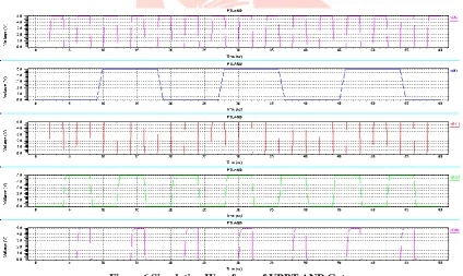
(B) VBBT based OR Gate along with sleep insertion technique
IJEDR1503056 International Journal of Engineering Development and Research (www.ijedr.org) 5 Figure 7 Schematic diagram of VBBT OR gate with sleep insertion technique
Figure 8 Simulation waveforms of VBBT OR gate
IV EXPERIMENTAL RESULTS
The leakage power is measured using the Tanner Tool S-EDIT simulator. The results obtained through the technique for logic gates are shown in Table 1. Simulation for the logic gates are performed by taking process parameter, 90nm CMOS Technology.
Table-1
Gate Type Propagation Delay(ns) Power consumption(pw) %age reduction in power consumption Conventional VBBT Conventional VBBT
AND Gate 4 4.09 0.087 0.069 20
OR Gate 4.18 4.08 0.29 0.122 58
V. CONCLUSION
© 2015 IJEDR | Volume 3, Issue 3 | ISSN: 2321-9939
IJEDR1503056 International Journal of Engineering Development and Research (www.ijedr.org) 6 insertion technique and the other is variable body biasing technique. VBBT achieves the reduction in leakage power compared to other leakage reduction techniques, such as sleep transistor, sleepy keeper, etc. The performance has been investigated using 90nm Technology and evaluated by the comparison table 2 of the simulation result obtain from TSPICE.
REFERENCES
[1] Ajay Kumar Dadoria and Kavita Khare “ A novel approach for leakage power reduction technique in 65nm technologies”, International journal of VSI design and communication systems Vol.5, No.3, June 2014.
[2 John F. Wakerly, “Digital Design- Principles and Practices” , fourth edition.
[3] M. D. Powell, S. H. Yang, B. Falsafi, K. Roy, and T. N. Vijaykumar, “Gated-Vdd: A circuit technique to reduce leakage in deep submicron cache memories,” in Proc. IEEE ISLPED, 2000, pp. 90-95.
[4] Tezaswi Raja and Michael L. Bushnell ,” Variable Input Delay CMOS Logic for Low Power Design”. .IEEE Transcations on very large scale integration (VLSI) systems Vol 17. No. 10. October 2009.
[5] Sarvesh Bhardwaj and Sarma Vrudhula .” Leakage Minimization of Digital Circuits Using Gate Sizing in the Presence of Process Variations ”.IEEE Transactions on computer –aided design of integrated circuits and systems. Vol. 27. No. 3 , March 2008.
[6] M. Powell, S.-H. Yang, B. Falsafi, K. Roy and T. N. Vijaykumar, “Gated-Vdd: A Circuit Techniqueto Reduce Leakage in Deep submicron Cache Memories,” International Symposium on Low Power
Electronics and Design, July 2000, pp. 90-95.
[7] Yuanlin Lu and Vishwani D. Agrawal “CMOS Leakage and Glitch minimization for power performance tradeoff ” Department of Electrical and Computer Engineering, Auburn University, Auburn, AL 36849, USA. Journal of Low Power Electronics vol. 2, 1-10, 2006.
[8] S. H. Kim and V. J. Mooney, “Sleepy Keeper: a new approach to low-leakage power VLSI design,” IFIP, pp. 367-372, 2006. [9] Bagadi Madhavi, G Kanchana, Venkatesh Seerapu “Low Power and Area Efficient Design of VLSI Circuits” International Journal of Scientific and Research Publications, Volume 3, Issue 4, April 2013, ISSN 2250-3153.
[10] B. S. Deepak subramanyan and A. Nunez, “Analysis of Sub threshold Leakage Reduction in CMOS Digital Circuits,” Proceedings of the 13th NASA VLSI Symposium, Post Falls, 5-6 June 2007, pp. 1-8.
[11] R. X. Gu and M. I. Elmasry, “Power Dissipation Analysis and Optimization of Deep Submicron CMOS Digital Circuits” IEEE Journal of Solid-State Circuits, Vol. 31, No. 5, 1996, pp. 707-713. http://dx.doi.org/10.1109/4.509853.
[12] Y.Taur, T.H. Ning, “Fundamentals of Modern VLSI Devices”, Cambridge University Press, New York, 1998.
[13] International Technology Roadmap for Semiconductor (ITRS-05). http://www.itrs.net/ Links/ 2005ITRS/Design2005.pdf. [14] D. Lee, W. Kwong, D. Blaauw and D. Sylvester, “Analysis and Minimization Techniques for Total Leakage considering Gate Oxide Leakage" In Proceedings of the 40th Design Automation Conference, pp. 175-180, Anaheim, 2003.
[15] P. Verma, R. A. Mishra, “Leakage power and delay analysis of LECTOR based CMOS circuits”, Int’l conf. on computer & communication technology ICCCT 2011.