Implementation of Single Precision Floating
Point Processor Using Residue Number
System
Elby C Varghese
1, Merlin Thomas
2PG Student [VLSI], Dept. of ECE, Viswajyothi College of Engineering and Technology, Ernakulam, Kerala, India1
Assistant professor, Dept. of ECE, Viswajyothi College of Engineering and Technology, Ernakulam, Kerala, India2
ABSTRACT: The use of floating point unit has lot of application in real time embedded systems. Algorithms like fast fourier transform (FFT) from the digital signal processing (DSP) domain often make extensive use of floating point arithmetic. This paper presents the design and implementation of a single precision floating point processor using residue number system (RNS) in FPGA. This processor uses Microprocessor without Interlocked Pipeline Stages (MIPS) instruction set architecture. It is capable of performing both floating point as well as integer operations . The design is done in a way to optimize the performance of the processor using the attractive properties of residue number system such as parallelism and carry free computation. The design is coded in Verilog hardware description language and synthesized with the help of Xilinx ISE tool.
KEYWORDS: Residue Number System, Floating Point Processors, FPGA.
I.INTRODUCTION
Floating-point arithmetic is widely used in many areas, especially in scientific computation, numerical processing and signal processing. Due to progression in VLSI technology nowadays FPGA's with high speed, more embedded modules and more number of logic are available. These make them suitable for implementing complex applications like floating point arithmetic. If the performance of floating point arithmetic in FPGA is improved, then FPGA is an attractive platform for scientific and real time applications.
With this goal of flexibility in mind, the processor is designed in such a way that it can be configured to perform several useful functions. Since multiplication, subtraction and addition are three of the most commonly used arithmetic operations, these operations are included in the Floating Point Arithmetic and Logic Unit, both in integer and floating-point mode. Along with this, logic operations on integers are also included in the proposed floating floating-point processor. This processor has separate data memory and program memory, 32 number of 32 bit register file, 32 bit A and B registers, 32 bit program counter (PC) and 32 bit instruction register (IR). For the effective implementation of the arithmetic operations on floating point and integer numbers, a residue number system (RNS) based floating point ALU is proposed for the processor. The design is coded using verilog HDL and synthesized for Xilinx virtex-4 device. The design is synthesized using Xilinx ISE tool.
II. RELATED WORK
There are different types of processors. They are discrete processors, hard core processors and soft core processors
.
The first step in designing a processor is choosing an efficient instruction set architecture for our processor. Two architectures available are Reduced Instruction Set Computer (RISC)[1] and Complex Instruction Set Computer (CISC) architecture.
A Floating point ALU is a processor or part of a processor that performs floating point calculations. When without a floating point unit, a CPU can handle both integer and floating point calculations. However, integer operations use significantly different logic than floating point operations, which makes it inefficient to use the same processor to handle both types of operations. An FPU provides a faster way to handle calculations with non-integer numbers. To design a Floating Point Unit we can follow different approaches like, Separate paths for multiplier and adder, merging common datapaths of multiplier and adders, use of effective algorithm for individual component design[2] or use multimode operations[5].
III.
SINGLE PRECISION FLOATING POINT PROCESSOR DESIGNThe IEEE754 standard floating point format consists of three fields, a sign bit (s), a biased exponent (e) and a mantissa (f).And Single-precision numbers have a 1-bit sign, 8-bit exponent, and 23-bit mantissa.The first step in design is choosing an efficient instruction set architecture for the processor. Here MIPS ISA (instruction set architecture) is used. MIPS is a load-store RISC (Reduced Instruction Set Computer) instruction set with three operands. Remaining of the design is divided into datapath and controller design.
Instructions included are:Register (R-type): Floating point addition, integer addition, Floating point multiplication, integer multiplication, Floating point subtraction, integer subtraction, logic operation like AND, OR, NOT, XOR, XNOR, NAND and NOR.(I-type): load, store, integer addition immediate, subtraction immediate, multiplication immediate and jump.Here the Instructions are 32 bit long, with a six bit opcode. And the instruction set uses three address instruction format. Two types of instruction are implemented in this design. They are R-type instruction and I type. The instructions are shown in table 1.
Table 1. Instructions
Instruction Operation
Load Load data from data memory to file register
Store The data in the file register is stored to date memory
FP Addition/ Subtraction/
Multiplication
Floating point addition/subtraction is performed on two operands
from the file register and the result is stored back to the
destination register
Integer Addition/
subtraction/multiplication
Normal addition/ subtraction/multiplication is performed on two
operands from the file register and the result is stored back to the
destination register
ImmediateAddition/ Subtraction/
Multiplication
Normal addition/ Subtraction/ Multiplication is performed on two
operands, one from the file register and other from the immediate
field and the result is stored back to the destination register
AND/ OR/ NOT/ NAND/ NOR/ XOR/
XNOR
Performs bitwise operation on two operands from the file
register and the result is stored back to the destination register
IV. DATAPATH DESIGN
Here the datapath is based on MIPS. It also utilizes the features of the Harvard architecture (separate memory for instruction and data). In this scheme instructions are executed in multiple clock cycles. In a multicycle implementation, each step in the execution will take 1 clock cycle. The ability to allow instructions to take different numbers of clock cycles and the ability to share functional units within the execution of a single instruction are the major advantages of a multicycle design.
The datapath consist of separate data memory and program memory. It also consist of 32 number of 32 bit register file, 32 bit A and B registers, 32 bit floating point arithmetic and logic unit with integer support. The datapath is divided into fetch, decode and execute/memory access and write back. And operation of each section is controlled by the control signal generated from the controller. The fig. 1 shows the high-level view of the multicycle datapath.
Fig. 1 High-level view of the multicycle datapath.
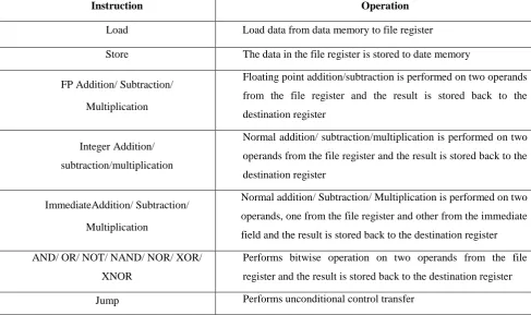
V.CONTROL UNIT DESIGN
The control unit of the MIPS processor examines the instruction opcode bits [31:26] and decodes the instruction to generate control signals to be used in the datapath. Here the controller uses FSM to generate the control signal. A finite state machine consists of a set of states and directions on how to change states. The directions are defined by a next-state function, which maps the current next-state and the inputs to a new next-state. While using a finite next-state machine for control, each state also specifies a set of outputs that are asserted when the machine is in that state.
Fig. 2 FSM control for datapath
After the execution of the last step for a particular instruction class, the finite state machine will return to the initial state to begin fetching the next instruction. Fig.2 shows this abstracted representation of the finite state machine.
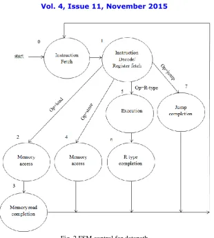
VI. RESIDUE NUMBER SYSTEM BASED FLOATINGPOINT ALU
The Floating point unit (FPU) used in this processor is the residue number system based FPU. It is a single precision IEEE-754 compliant integrated unit. It can handle basic floating point operations like floating point addition, subtraction and multiplication in floating point mode and 23 bit normal addition, subtraction, multiplication, AND, OR, NOT, XOR, XNOR, NAND and NOR in integer mode of operation.
Fig. 3 RNS Floating Point Arithmetic Unit Architecture
Fig. 4 shows the block diagram of RNS adder and RNS multiplier. The modulo multiplication is done using brickell‟s algorithm. The modulo addition is done using modulo adders. The adder, subtractor and multiplier for mantissa are used for performing integer addition, subtraction and multiplication. The subtraction is done as two‟s complement addition.
Forward Converter/ Binary to RNS converter
The data available will be in the form of binary. In order to process in RNS, the binary data has to be converted into RNS. The process of converting binary data into RNS is referred to as the forward conversion. The forward conversion can be for an arbitrary moduli set or special moduli set. The special moduli set used in this paper include {2" -1, 2", 2" + 1} where n is decided based on the number of bits of the input binary number. These special moduli set are considered for the RNS operation because they make the system fast and simple along with being efficient.Due to the usage of a special moduli set, {2" -1, 2", 2" + 1} the number to be converted to RNS is divided into three blocks each of „n‟ bits. The three blocks B1, B2, B3 are represented as given below.
B1 = 2𝑗 −2𝑛
3𝑛 −1
𝑗 =2𝑛 𝑥𝑗B2 = 2
𝑗 −𝑛 2𝑛−1
𝑗 =𝑛 𝑥𝑗B3 = 2
𝑗 𝑛 −1 𝑗 =0 𝑥𝑗
Thus, the input binary number, X can be given in terms of the blocks as,
𝑋 = 𝐵122𝑛+ 𝐵22𝑛+ 𝐵3
Then the residues can be obtained as follows,
𝑟1= |𝐵122𝑛+ 𝐵22𝑛+ 𝐵3 |2n-1
𝑟2= 𝐵3
𝑟3= |𝐵122𝑛+ 𝐵22𝑛+ 𝐵3 |2 n
+1
Where, the modulo-m addition is done as follows.
| X + Y |m =
𝑋 + 𝑌 ∶ 𝑋 + 𝑌 < 𝑚 𝑋 + 𝑌 − 𝑚 ∶ 𝑋 + 𝑌 ≥ 𝑚
Reverse converter/ RNS to binary converter
RNS to binary conversion is the bottle neck in using RNS. They are mixed radix conversion (MRC) and Chinese remainder theorem (CRT). MRC is sequential whereas CRT is parallel. The design of modulo M adder in the final stage of CRT is design bottleneck of it. It is a tedious process to design modulo M adder, so in this project New Chinese Remainder Theorem is used for conversion of RNS to binary. Using New Chinese Remainder theorem, binary number X can be calculated as follows, where r1, r2, r3 are the residues.
X= r2 + 2𝑛* Y
Y = | 𝐴 + 2𝑛 * Y |
22n-1
A =
⌊
( (𝑟1+(𝑟10 xor 𝑟30) ∗ 2𝑛)+ (2𝑛 −1−𝑟
3) +(2𝑛 −1))
2
⌋
B =
⌊
((𝑟1+(𝑟10 xor 𝑟30) ∗ 2𝑛)+ 𝑟
3 + 2(2𝑛 −1−𝑟2))
2
⌋
VII. RESULT AND DISCUSSION
Upon reset the program counter is initialized to location zero of the instruction memory. The instruction is executed in multiple clock cycles. After one instruction is executed the program counter is incremented by one and next instruction is fetched from instruction memory in a sequential manner. A simple program to add and multiply two floating point numbers is stored in program memory and corresponding floating point data is stored in data memory.
Table 2 shows a set of instruction to perform floating point addition and multiplication operation. It includes two load instruction, a Floating point addition instruction and a Floating point multiplication instruction to perform floating point multiplication of two single precision numbers.
Table 2. ISA for addition and multiplication
For different arithmetic operations the opcode fields vary as well as the register also may vary according to the instruction. The opcode for floating point multiplication is „001000‟, for floating point addition it is „000000‟ and „001100‟ for load operation.
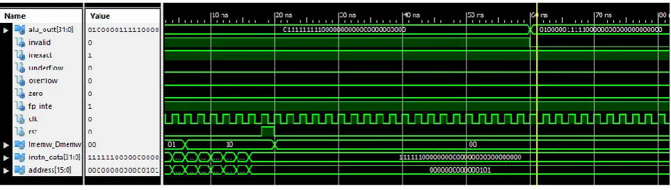
Fig. 5 Floating Point Processor output
And fig. 5 shows the simulation waveform of single precision floating point processor using residue number system. The waveform is obtained while performing the set of instructions given in table 2.
Load R0
0 0 1 1 0 0 00000 00000 000000000000000
Load R1
0 0 1 1 0 0 00000 00001 000000000000001
FP addition R0,
R1, R3 0 0 0 0 0 0 00000 00001 00011 00000000000
FP multiplication
R0, R3, R4
0 0 0 1 0 0 00000 00011 00100 00000000000
Fig. 6 shows design summary of Single precision Floating point processor using RNS after synthesis using Xilinx tool.
It helps to understand the FPGA device utilization in terms of slices, flipflops, LUTs and IOBs.
Fig. 6 Design Summary Single precision Floating point processor using RNS
VIII.CONCLUSION
This paper deals with development of an efficient Floating Point Processor. In this project a Single precision Floating Point Processor with Residue Number System based ALU is designed. The ALU is capable of performing both floating point and integer operations. Here the attractive properties of residue number system such as parallelism and carry free computation are used to enhance the performance of the processor. Here the processor uses MIPS and Harvard based architecture. The efficiency is again improved by reconfiguring the datapath for two modes of operation, integer mode and floating point mode. The design is coded in verilog hardware description language and synthesized with the help of Xilinx ISE tool.
REFERENCES
[1] R. Anjana and Krunal Gandhi, “VHDL Implementation of a MIPS RISC Processor”, International Journal of Advanced Research in Computer Science and Software Engineering, vol. 2, Issue 8, ISSN: 2277 128X, August 2012.
[2] Barathi V, R Dhanabal, Naamatheertham R Samhitha, NeethuAcha Cherian, Pretty Mariam Jacob and Sarat Kumar Sahoo, “Implementation of Floating Point Mac Using Residue Number System”, IEEE International Conference on Reliability, Optimization and Information Technology (ICROIT), pp461-465, February 2014.
[3] M. Dugdale, “VLSI implementation of residue adders based on binary adders”, IEEE Transactions on Circuits and System II: Analog and Digital Signal Processing, vol. 39, no. 5, pp. 325- 329, May 1992.
[4] Alpesh Kumar Dauda, Nalinikanta, BarpandaNilamaniBhoi and Manoranjan Pradhan, “Control Unit Design of a 16-bit Processor Using VHDL”, International Journal of Advanced Research in Computer Science and Software Engineering, vol. 3, Issue 12, ISSN: 2277 128X, December 2013.
[5] Yee Jern Chong and Sri Parameswaran, “Configurable Multimode Embedded Floating-Point Units for FPGAs”, IEEE Transactions On Very Large Scale Integration Systems, Vol. 19, No. 11, November 2011.
[6] PakkiraiahChakali, Madhu Kumar Patnala, “Design of High Speed Kogge Stone Based Carry Select Adder”, International Journal of Emerging Science and Engineering (IJESE) ISSN: 2319-6378, Volume1, Issue-4, February 2013.
[7] Wei Wang, M.N.S. Swamy, M. O.Ahmad and Yuke Wang, “The Applications of the New Chinese Remainder Theorems for Three Moduli Sets”, Proceedings of the IEEE Canadian Conference on Electrical and Computer Engineering, vol.1, ISSN : 0840-7789, pp. 571 - 576,May 1999.
[8] David A. Patterson and John L. Hennessy, “Computer Organization Design: The hardware/software interface”, Morgan Kaufmann publications, 3rd edition, ISBN: 1-55860-604-1,2005.
[9] BehroozParhami, “Computer arithmetic Algorithms and hardware designs”, Oxford University Press, 2000.
BIOGRAPHY
Elby C Varghese was born in India, on August 08, 1990. She graduated from the College of Engineering Kallooppara, Kerala, India in Electronics & Communication Engineering (2012). She is now pursuing Master of Technology in VLSI and Embedded Systems from Viswajyothi College of Engineering and Technology, Ernakulam, kerala, India. Her special fields of interest include VLSI and Embedded System Design.