Adiabatic Array Logic Design of 4x1 MUX
and 8x1 MUX without Redundancy
Shivangini1, Yamini Verma1, Ashwani Kumar2
PG Student [VLSI Design], Dept. of ECE, IGDTUW, Kashmere Gate, New Delhi, India1
Professor, Dept. of ECE, IGDTUW, Kashmere Gate, New Delhi, India2
ABSTRACT:Adiabatic array logic allows designing low power digital circuits with more power saving despite having an equal number of transistors with the conventional CMOS logic style and 2PASCL In this paper, 4x1 MUX and 8x1 MUX is designed using Adiabatic Array Logic and by removing redundant transmission gates from Adiabatic Array Logic. The proposed designed shows the reduced power dissipation and also transistor count in comparison with basic Adiabatic Array Logic design. The comparison of power dissipation is also carried out with sinusoidal power supply over a frequency range of 100MHz-600MHz. The simulations are carried out in Cadence Virtuoso at 180nm technology, 1.8V CMOS standard process technology.
KEYWORDS: Adiabatic logic; Adiabatic Array Logic; charge recovery; power consumption; redundancy; power saving
I.INTRODUCTION
The increasing demand of mobile devices and the need to limit power consumption in VLSI chips led to rapid and innovative developments in low power circuit design during recent years [6]. The main motive behind these developments is mobile devices requiring low power consumption and high throughput. In low power design techniques, adiabatic logic circuits break the lower limit of the energy dissipation in static CMOS which equals to C
2 DD
V
/2 by using AC power supply instead of the DC power supply. There are several adiabatic logics [4][7][8] have been developed in several years. Adiabatic Array Logic [1][2][3] is new adiabatic technique which is recently proposed. It employs an AND plane of transmission gates to realize ANDed terms and a wired OR-plane to OR them. Before the actual work is discussed, a brief theory of adiabatic and CMOS logic along with Adiabatic Array Logic is shown.Consider a CMOS inverter with DC supply voltage
V
DD. The energy dissipation during charging/discharging cycle of load capacitance is given by2 2 1
DD L CMOS C V
E (1)
where α is the switching probability.
In adiabatic inverter circuit, the energy dissipation during charging/discharging is given by:
2
_diss 2 DD adia CV
T RC
E (2)
RC
T
CV
CV
T
RC
DD DD
4
2
1
2
2 2
As adiabatic logic aims to minimize the energy dissipation, we have to:
CMOS
AL
E
E
Or
Or (3)
This condition is required for adiabatic logic to better than the static CMOS logic. The physical significance of equation (3) is that the charging time T of the capacitor should be high i.e., the charging process should be slow. This is achieved by using a AC supply such as ramp or sinusoidal voltage instead of the DC voltage.
Figure 1. Ramp voltage Figure 2. DC voltage
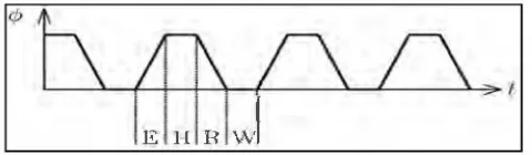
Ramp voltage used in adiabatic logic is called the power clock. It has four intervals: evaluate (E), hold (H), recover (R) and wait (W), as shown in Fig.3.
Fig.3. Phase in an Adiabatic Power Supply
The adiabatic array logic is driven by a sinusoidal power supply, the power clock. The logic is shown below:
It consists of an array of transmission gates to form AND plane and wired OR plane. This circuit can be analyzed by transmission gate in the ON state represented with a linear model made up of a resistance R and a capacitance C [5] at the output node as shown in Fig.4.
) ln( 1 ) ln( 1 ) ln( 1 1 n n n p p p n n ox n p p ox p tp tn DD tp DD p p ox p tp tn DD tn DD n n ox n DD L W L W L W C L W C V V V V V L W C V V V V V L W C V R (4)
Assuming the triode region for both PMOS and NMOS transistors, the capacitance C is given by:
CON W LL)Cox CjB
2 1
( (5)
where, ∆L is the overlap and capacitance
C
jBis due to the junction between the diffusion and the bulk.II.PROPOSED WORK
The Adiabatic Array Logic designs have some repeated transmission gates which consumes area as well as power. Therefore it is necessary to make the adiabatic array logic redundant. Here, we have taken two circuits 4x1 MUX and 8x1 MUX to compare basic Adiabatic Array Logic and Redundant Adiabatic Array Logic.
A multiplexer [10][15] (or MUX) is a device that selects one of several input signals and forwards the selected input into a single line. A multiplexer of 2n inputs has n select lines, which are used to select which input line to send to the output.
4x1 Multiplexer has 4 inputs, 2 select lines and 1 output line. The select lines select one of the data and give it to the output. The expression for the 4x1 MUX is shown below:
Y S1S0I0S1S0I1S1S0I2S1S0I3 (6)
8x1 Multiplexer has 8 inputs, 3 select lines and 1 output line. The select lines select one of the data and give it to the output. The expression for the 8x1 MUX is shown below:
3 0 1 3 2 0 1 3 1 0 1 3 4 0 1 3 3 0 1 3 2 0 1 3 1 0 1 3 0 0 1 3 I S S S I S S S I S S S I S S S I S S S I S S S I S S S I S S S Y
(7)
load capacitance 0.01pF. Simulating these circuits provided the output waveforms, below their respective circuits. Four terminal MOS transistors have been used whose substrate is connected to VDD and ground for PMOS and NMOS respectively.
Fig.5(a).4x1 MUX using Adiabatic Array Logic
Fig.6(a). Proposed 4x1 MUX Adiabatic Array Logic without redundancy
Fig.7(a).8x1 MUX using Adiabatic Array Logic
Fig.8(a). Proposed 8x1 MUX Adiabatic Array Logic without redundancy
III.RESULTS AND DISCUSSION
The total power dissipation of any circuit can be defined as the sum of the products of the voltage and current of all power sources present within the circuit. To calculate the power savings in the circuits, the energy consumption E is computed as below:
dt
I
V
E
s T n i pi pi
0 1 (8)Where
T
s(=1/f
s) = the period of the primary input signal;V
p = the power supply voltage,I
p= the power supply current, and i = number of power supply. Therefore, energy dissipation E is equal to the net energy flowing into the circuit from the power supply.The propagation delay [5] of the circuit should be considered to measure performance of the circuit. The transmission gate can be modelled as an ohmic series resistance R bounded by capacitance by two grounded
capacitance C. The step response delay
t
DRC of chain of RC element is given by
n i i i RCD
R
C
t
0
where i is no of node. (10)
The total power dissipation and propagation delay of the proposed circuit and basic Adiabatic Array Logic circuits are evaluated by doing transient analysis at different frequency ranging from 100 MHz to 600 MHz of sinusoidal power supply. Area per chip is calculated by formula W*L*Transistor count.
TABLE I. PERFORMANCE ANALYSIS OF ADIABATIC ARRAY LOGIC STYLE AND CMOSLOGIC STYLE FOR 4X1MUX AND ADIABATIC ARRAY LOGIC WITHOUT REDUNDANCY
Parameter Adiabatic Array
Logic CMOS logic
Adiabatic Array Logic without
redundancy
Transistor count 24 24 20
Area per chip(μm2) 2.594 2.594 2.16
Total Power Dissipation(μW) at 200 MHz 5.316 7.452 5.121
Delay at 200MHz 6.023 5.359 5.976
TABLE II. POWER DISSIPATION OF ADIABATIC ARRAY LOGIC STYLE AND PROPOSED ADIABATIC ARRAY LOGIC 4X1 MUX AT DIFFRENT FREQUENCY OF SINUSOIDAL POWER SUPPLY
Frequency of Sinusoidal Power Supply (MHz) Total Power Dissipation(μW
) of Adiabatic
Array Logic
Style
Total Power
Dissipation
(μW) of Adiabatic
Array Logic Style
Without
redundancy
Propagation Delay(ns)
of Adiabatic Array Logic
Propagation Delay(ns) of
Adiabatic Array Logic
Without redundancy
Frequency
of
Sinusoidal
Power
Supply
(MHz)
Total Power
Dissipation(μW
) of Adiabatic
Array Logic
Style
Total Power
Dissipation
(μW) of Adiabatic
Array Logic Style
Without
redundancy
Propagation Delay(ns)
of Adiabatic Array Logic
Propagation Delay(ns) of
Adiabatic Array Logic
Without redundancy
200 5.316 5.121 6.023 5.976
300 8.484 5.943 7.385 7.331
400 9.770 7.422 5.586 5.545
500 12.640 8.667 5.512 5.465
600 16.070 10.730
5.418 5.412
TABLE III. PERCENTAGE CHANGE OF PARAMETERS OF PROPOSED DESIGN WITH RESPECT TO VARIOUS LOGIC STYLE FOR 4X1MUX
Parameter Adiabatic Array Logic CMOS logic
Transistor count 20% Less 20% Less
Area per chip(μm2) 20.09% Less 20.09% Less
Total Power Dissipation(μW)
at 200 MHz
3.81% Less 45.51% Less
Delay at 200MHz 0.78% Less 10.32% More
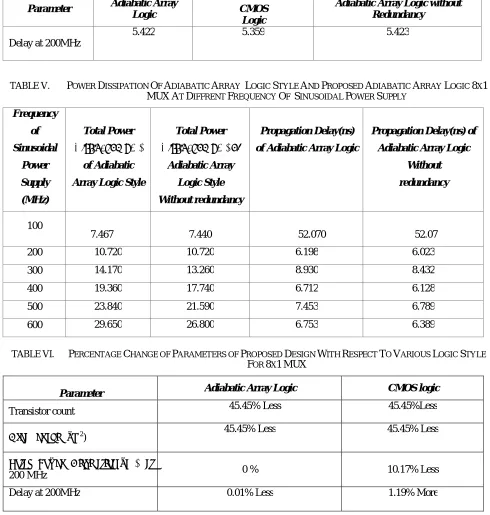
TABLE IV. PERFORMANCE ANALYSIS OF ADIABATIC ARRAY LOGIC STYLE AND CMOSLOGIC STYLE FOR 8X1MUX AND ADIABATIC ARRAY LOGIC WITHOUT REDUNDANCY
Parameter Adiabatic Array
Logic CMOS
Logic
Adiabatic Array Logic without Redundancy
Transistor count
644 64 444
Area per chip(μm2) 6.912 6.912 4.752
Total Power Dissipation(μW) at 200 MHz
Parameter Adiabatic Array
Logic CMOS
Logic
Adiabatic Array Logic without Redundancy
Delay at 200MHz
5.422 5.359 5.423
TABLE V. POWER DISSIPATION OF ADIABATIC ARRAY LOGIC STYLE AND PROPOSED ADIABATIC ARRAY LOGIC 8X1 MUXAT DIFFRENT FREQUENCY OF SINUSOIDAL POWER SUPPLY
Frequency
of
Sinusoidal
Power
Supply
(MHz)
Total Power
Dissipation(μW)
of Adiabatic
Array Logic Style
Total Power
Dissipation(μW) of
Adiabatic Array
Logic Style
Without redundancy
Propagation Delay(ns)
of Adiabatic Array Logic
Propagation Delay(ns) of
Adiabatic Array Logic
Without
redundancy
100 77.467.467
7
7.440 5252.070 552.07
200 10.720 10.720 6.198 6.023
300 14.170 13.260 8.930 8.432
400 19.360 17.740 6.712 6.128
500 23.840 21.590 7.453 6.789
600 29.650 26.800 6.753 6.389
TABLE VI. PERCENTAGE CHANGE OF PARAMETERS OF PROPOSED DESIGN WITH RESPECT TO VARIOUS LOGIC STYLE FOR 8X1MUX
Parameter Adiabatic Array Logic CMOS logic
Transistor count 4545.45% Less 45.45%Less
Area per chip(μm2) 45.45% Less 45.45% Less
Total Power Dissipation(μW) at
200 MHz 0 % 10.17% Less
Delay at 200MHz 0.01% Less 1.19% More
VI.CONCLUSION
frequency, these circuits dissipate larger power. Though the propagation delays of these circuits are higher up to small content, these circuits are reliable with low frequency.
REFERENCES
[1] Tomita.Y, Takahashi.Y, Sekine, T., "Adiabatic array logic," Signals and Electronic Systems (ICSES), 2010 International Conference on, vol.no., pp. 269,272, 7-10 Sept. 2010.
[2] Shruti Konwar, Thockchom Birjit Singha, Soumik Roy, “Power Efficient Code Converters Using Adiabatic Array Logic”, 2014 Fourth International Conference of Emerging Applications of Information Technology on pp. 167-172, 19-21 Dec. 2014.
[3] Thockchom Birjit Singha, Shruti Konwar, Soumik Roy, “Low Power Design and Analysis of Fundamental Logics Using Adiabatic Array Logic Low Power Design and Analysis of Fundamental Logics Using Adiabatic Array Logic”, 2014 International Conference on Signal Propagation and Computer Technology (ICSPCT) on pp.775-781,12-13 Jul. 2014.
[4] Anuar.N, Takahashi.Y, Sekine.T, "Two phase clocked adiabatic static CMOS logic," System-on-Chip, 2009. International Symposium on, vol., no., pp.083, 086, 5-7 Oct. 2009.
[5] Alioto, M.; Palumbo, G., "Power estimation in adiabatic circuits: a simple and accurate model," Very Large Scale Integration (VLSI) Systems. IEEE Transactions on, vol.9, no.5, pp.608,615, Oct. 2001.
[6] William C. Athas, Lars J. Svensson, Jeffrey G. Koller, Nestoras Tzartzanis, and Eric Ying-Chin Chou, “Low-Power Digital Systems based on Adiabatic switching Principles”, IEEE Transactions On Very Large Scale Integration (VLSI) Systems, VOL. 2, NO. 4, Dec.1994.
[7] A. K. Bakshi and M. Sharma, "Design of basic gates using ECRL and PFAL," 2013 International Conference on Advances in Computing, Communications and Informatics (ICACCI), Mysore, 2013, pp. 580-585.
[8] Yong Moon and Deog-Kyoon Jeong, "An efficient charge recovery logic circuit," in IEEE Journal of Solid-State Circuits, vol. 31, no. 4, pp. 514-522, Apr 1996.
[9] M. L. Keote and P. T. Karule, "Design and implementation of energy efficient Adiabatic ECRL and basic gates," 2015 International Conference on Soft Computing Techniques and Implementations (ICSCTI), Faridabad, 2015, pp. 87-91.
[10] Arun Kumar, Manoj Sharma, “Design and analysis of MUX using adiabatic techniques ECRL and PFAL”, International Conference on Advances in Computing, Communications and Informatics (ICACCI), pp.1341-1345, 2013.
[11] P. Bhati and N. Z. Rizvi, "Adiabatic logic: An alternative approach to low power application circuits," 2016 International Conference on Electrical, Electronics, and Optimization Techniques (ICEEOT), Chennai, India, 2016, pp. 4255-4260.
[12] A. K. Kumar, D. Somasundareswari, D. Duraisamy and G. Sabarinathan, "Asynchronous design of energy efficient full adder," 2013 International Conference on Computer Communication and Informatics, Coimbatore, 2013, pp. 1-6
[13] Anuar, N., Takahashi, Y., Sekine, T., "XOR evaluation for 4×4-bit array two-phase clocked adiabatic static CMOS logic multiplier," Circuits and Systems (MWSCAS), 2010 53rd IEEE International Midwest Symposium on , vol., no., pp.825,828, 1-4 Aug. 2010.
[14] Anuar, N.Takahashi, Y. Sekine, T., "4-bit ripple carry adder using two phase clocked adiabatic static CMOS logic," TENCON 2009 – 2009 IEEE Region 10 Conference, vol., no., pp.1,6, 23-26 Jan. 2009.
[15] Leach Donald P., “Digital Principles and Applications”, Tata Mcgraw Hill Education Private Limited, 2010 Edition.