1515 | P a g e
Analysis and Design of MOS Current Mode Logic
Circuits with Active Inductor Load
Kirti Gupta
.1, Neeta Pandey
21Dept. of Electronics and Communication, Bharati Vidyapeeth’s College of Engineering, Delhi, India 2
Dept. of Electronics and Communication Engineering, Delhi Technological University, Delhi, India
ABSTRACT
This paper presents the analysis and design of an improved version of conventional MOS current mode logic (MCML) known as the shunt-peaked MCML style (MCML-SP) is presented. This logic style employs inductors in the load. The analytical formulation of the shunt-peaked MCML inverter employing active inductor is derived. An approach to design shunt-peaked MCML inverter is also developed which is easily extended to realize complex shunt-peaked digital MCML circuits. The performance of the designed circuits is compared with their respective MCML counterparts through simulations using TSMC 0.18 µm CMOS technology parameters. A maximum delay reduction of 29 % is achieved for shunt-peaked MCML circuits. The impact of process variation on the MCML-SP and conventional MCML inverter at different design corners shows similar variations.
Keywords: Active Inductor, High-Speed,Digital Circuits, MCML, Shunt-Peaked
I INTRODUCTION
The tremendous advancements in the VLSI technology has led to the design of high-resolution mixed-signal applications. These applications demands high performance digital circuits to be fabricated with analog circuitry on the same silicon substrate. MOS current mode logic (MCML) style has been widely used to design of digital circuits for mixed-signal applications as they provide an analog friendly environment due to the low switching noise [1-6].
1516 | P a g e The paper first presents an overview of the conventional MCML style in section 2. Then, the analysis of the shunt-peaked MOS current mode logic style employing active inductors is presented in section 3. An approach to design peaked MCML inverter is formulated in section 4 which is extended for shunt-peaked digital circuits. A variety of digital circuits is designed and is compared with the conventional MCML counterparts through simulations using 0.18 µm TSMC CMOS technology parameters in section 5. The impact of process variation at different design corners is also studied. Finally section 6 concludes the paper.
II MOS CURRENT MODE LOGIC (MCML) STYLE
A conventional MCML circuit consists of three main parts: a pull-down network (PDN), a constant current source, and a load circuit. The PDN implements the logic function by applying the series-gating approach [4]. The constant current source MC1 provides the bias current ISS while the load resistor RL determines the voltage swing. A schematic of a conventional MCML inverter with differential input A is shown in Fig.1. It works on the principle of current steering. When the differential input A is high, the bias current ISS flows through the transistor MC2 and produces a low differential output voltage (VOL = VQ− V = − IQ ssRL).
Conversely, when the differential input A is low, the bias current ISS gets steered to transistor MC3 and produces a high differential output voltage (VOH = VQ− V = IQ ssRL). Thus, the voltage swing, VSWING defined as the difference in the high and low output voltage is given as:
VSWING = VQ− V = 2 IQ SSRL (1)
The voltage gain Av_con can be computed by applying the half circuit concept [11]. The analysis of Fig. 1b
gives Av_con as:
Av_con = VQ(s) VA(s)=
gmc 2RL
1+sRLCL (2)
where RL= load resistance, CLis the load capacitance including the parasitic capacitances of the transistors in
the PDN and the interconnect capacitances and gmc 2 is the transconductance of the transistor MC2.
1517 | P a g e (b)
Fig.1. Conventional MCML inverter (a) circuit diagram (b) equivalent half circuit
III SHUNT-PEAKED MCML STYLE
The shunt-peaking technique can be used to increase the speed of the conventional MCML circuits [8]. This technique uses an inductor (L) in series with a resistor (RSP) in the load such that the first-order RC circuit
(2) is replaced with a second-order (RLC) circuit. Such circuits are named as shunt-peaked MCML circuits and may be abbreviated as MCML-SP circuits. A schematic of a MCML-SP inverter employing spiral inductor in the load is shown in Fig.2. When the differential input A is high, the bias current ISS flows through the transistor MS2 and produces a low differential output voltage (VOL = VQ− V = − IQ ssRSP) as
the inductor L behaves as a short circuit to the constant inputs. Conversely, when the differential input A is low, the bias current ISS is steered to the transistor MS3 and produces a high differential output voltage (VOH = VQ− V = IQ ssRSP). Thus, for the equal values of RSP and RL, the voltage swing, VSWING of the MCML-SP circuits is same as that of the conventional MCML circuits.
The use of the spiral inductor has several restrictions such as large component size and lengthier design process. Therefore, an active inductor [8] can be used in place of spiral inductor as shown in Fig. 3. The schematic of a MCML-SP inverter employing the active inductor load along with its equivalent half circuit are shown in Fig. 4. The output impedance of the inverter, Zout _ac by neglecting substrate bias effect can be computed from Fig. 4b as:
Zout _ac =
s (Cgs 4+Cgd 4) +GBIAS
s2( Cgd 4Cgs 4+ CLCgs 4+ CLCgd 4)+s GBIAS CL+Cgs 4 + gma 4Cgd 4 + gma 4GBIAS
(3) where GBIAS(= 1 RBIAS ) is the conductance in the active inductor, CLis the load capacitance including the
1518 | P a g e
Fig.2. MCML-SP inverter with spiral inductor
Fig.3. active inductor [8]
(a)
(b)
Fig.4. MCML-SP inverter with the active inductor (a) circuit diagram (b) equivalent
half circuit
The derivation of the voltage gain Av_ac for the MCML-SP inverter with active inductor load using in the
1519 | P a g e Av_ac =
VQ s
VA s = gma 2Zout _ac
= gma 2 s (Cgs4+ Cgd 4) + GBIAS s2( C
gd 4Cgs4+ CLCgs4+ CLCgd 4) + s GBIAS CL+ Cgs4 + gma 4Cgd 4 + gma 4GBIAS
(4a) where gma 2 is the transconductance of the transistor MA2,
By assuming Cgd 4Cgs4 ≪ CL(Cgd 4+Cgs4), the (4a) can be simplified as:
Av_ac =
gma 2 s (Cgs 4+Cgd 4) +GBIAS
s2CL Cgs 4+Cgd 4 +s GBIAS CL+Cgs 4 + gma 4Cgd 4 + gma 4GBIAS
(4b) In standard form [12], (4b) can be rewritten as:
Av_sp(s) = s+z ωn
2 z
s2+ 2ςωns+ ωn2 (4c)
Comparing (8b) with (8c), the value of the damping factor and natural frequency can be computed as: damping factor, ς = 12(CL+ Cgs4+Ggma 4
BIAS Cgd 4)
GBIAS
Cgs 4+Cgd 4 CLgma 4 (5a)
For large values of CL, (9a) can be approximated as:
damping factor, ς = 12 CL GBIAS
Cgs 4+Cgd 4 gma 4 (5b)
natural frequency, ωn = Cgma 4GBIAS
gs 4+Cgd 4 CL (5c)
Depending on the value of the damping factor, ς, the circuit can be overdamped (ς > 1), critically damped (ς = 1) and underdamped (ς <1) and accordingly the time responses for the three cases differ. The presence of a LHP s-plane zero in (4a) further tends to enhance the speed of the MCML-SP inverter in comparison to conventional MCML inverter.
IV DESIGN OF MCML-SP CIRCUITS
1520 | P a g e
4.1 Design of MCML-SP inverter with active inductor load
For the active inductor MCML-SP inverter (Fig. 4), the output impedance derived in (3) reduces to 1/gma 4for the static case. By solving (1) and then equating to the impedance in the static case, the value of
aspect ratio of the load transistors MA4 and MA5 for the given values of the bias current ISS and the voltage swing VSWING, can be calculated as
WN
LN MA 4,5=
2 ISS
VSWING µeff ,nCox VDD−VT,n (6) where the parameters µeff ,n , VT,n, WNand LNare the effective electron mobility, the threshold voltage, the
effective channel width and effective channel length of the load transistors MA4 and MA5 respectively. After determining the size of MA4 and MA5, the different capacitance values are computed. The gate-source capacitance Cgs is equal to the overlap capacitance between the gate and the source [4]. The gate-drain
capacitance Cgd is evaluated as the sum of the overlap capacitance and the intrinsic contribution associated
with its channel charge [4].
For a specific value of damping factor, ς and load capacitance CL, the value of the GBIAS can be computed by using (5b) as:
GBIAS = 4 ς2 Cgs 4
+Cgd 4 gma 4
CL (7)
The aspect ratio of the transistors MA2 and MA3 in the PDN can be calculated by solving(3) for the static case.
WN
LN MA 2,3= Av_ac
2 WN
LN MA 4,5 (8)
4.2 MCML-SP digital circuit design
The design approach presented in section 4.2 for MCML-SP inverter design with active inductor loads can be extended to design other MCML-SP circuits. The steps to design the load for the active inductor load remain same as explained in section 4.2.To design the PDN, firstly the size of the equivalent inverter is found out by using either (12) or (15) depending upon the load and then individual transistors are sized according to the conventional approach for MCML circuits as discussed in [4].
V SIMULATION RESULTS
1521 | P a g e performed by using TSMC 0.18 µm CMOS technology parameters with a power supply of 1.8 V, bias current of 500 µA, voltage swing of 400 mV, and load capacitance of 400 fF.
5.1 Proposed MCML-SP Inverter
The methodology given in Section 3 and 4 is used to design active inductor load inverter with the outlined specifications for different damping factors. The simulations were performed to select the value of damping factor to achieve proper circuit operation and lowest propagation delay. The propagation delay for active inductor load inverter various values of damping factor, are listed in Tab. 1. It can be observed from the table that the propagation delay for the underdamped case is lower than the overdamped and the critically damped cases. For proper operation of the circuit, the overshoot should be less than 5% in the time response [12]. Keeping this in view, the case with ς = 0.7 gives the lowest propagation delay. Therefore, this value can be chosen as the optimum value to design MCML-SP circuits. The sizes of the transistors for the active inverter for ς = 0.7 are listed in Tab. 2. All the transistors have minimum channel length.
5.2 Performance Comparison
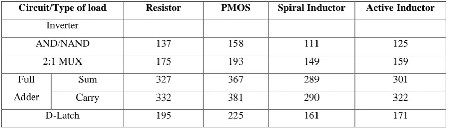
Several logic circuits such as AND/NAND, MUX, full adder, D-latch are designed with active inductor using the method outlined in section 4. The performance ofthese circuits is compared with their conventional resistive and PMOS [4], spiral inductor load MCML counterparts. It may be noted that all the circuits operate at same supply voltage and bias current therefore they all consume same static power computed as the product of the supply voltage and bias current [4]. The propagation delay of the gate with respect to the above loads is listed in Tab. 3. It can be noted that a delay reduction varying from 21% to 29% is obtained by using inductive load.
The impact of parameter variation on the MCML-SP inverters and the conventional inverters is studied at different design corners. The findings for various operating conditions are given in Tab. 4. It is found that the propagation delay varies by a factor of 1.04, 1.15, 1.11 and 1.10 for the resistive, PMOS, spiral inductor and active inductor load respectively between the best and the worst cases. It can be observed that they all show similar variations.
Table. 1. : Propagation delay of the MCML-SP inverter with active inductor loads for various values of
damping factor, ς
Damping factor, 𝛓 Propagation delay with active inductor (ps) Output response
2 120 Flat
1 111
0.9 108 Overshoots (< 5%)
0.8 104
1522 | P a g e
0.6 99 Overshoots (> 5%)
0.5 95
0.4 90
0.3 88
0.2 85
0.1 84
Table. 2. Values of the components for the MCML-SP inverter for ς = 0.7
MCML-SP inverter with active inductor load (Fig. 4a)
Component Value
MA1 W/L = 5.2 µm/0.18 µm
MA2, MA3 W/L = 17.5 µm/0.18 µm MA4, MA5 W/L = 8.65 µm/0.18 µm
RBIAS 7.34 KΩ
Table. 3. Comparison in Propagation delay (ps) of MCML logic circuits using different type of loads
Circuit/Type of load Resistor PMOS Spiral Inductor Active Inductor
Inverter
AND/NAND 137 158 111 125
2:1 MUX 175 193 149 159
Full Adder
Sum 327 367 289 301
Carry 332 381 290 322
D-Latch 195 225 161 171
Table 4. Impact of parameter variations on propagation delay (ps) for different inverters
NMOS
PMOS
Topology
T
T
F
F
S
S
F
S
S
F
Inverter with resistive load 127 125 130 129 128
Inverter with PMOS load 150 140 161 142 158
Inverter with spiral inductor load 100 95 106 105 104
1523 | P a g e
6
CONCLUSION
The analysis and design of shunt-peaked MCML style for digital circuit design is presented in this paper. The logic style uses the shunt-peaking technique and suggests the use of inductors in the load. The design method is illustrated for shunt-peaked MCML inverter with the spiral and active inductors. The effectiveness of the shunt-peaked MCML style is demonstrated by simulating different logic gates. It is found that the shunt-peaked MCML circuits are faster than the other MCML variants. The study of impact of process variation at different design corners shows that conventional MCML and MCML-SP inverters show similar variations.
REFERENCES
[1]Musicer J. M., Rabaey, J. MOS Current Mode Logic for Low Power, Low Noise, CORDIC Computation in Mixed-Signal Environments. In Proc. International Symposium of Low Power Electronics and Design, 2000, 102-107.
[2]Hassan, H., Anis, M., Elmasry, M. MOS Current Mode Circuits: Analysis, Design, and Variability. IEEE Transactions on Very Large Scale Integration (VLSI) Systems, 13(8),2005, 885 - 898.
[3]Nonis, R., Palumbo, E., Palestri, P., and Selmi, L. A Design Methodology for MOS Current-Mode Logic Frequency Dividers, IEEE Transactions on Circuits and Systems– II: Regular Papers, 54(2), 2007, 245-254.
[4]Alioto, M., Palumbo, G. Model and Design of Bipolar and MOS Current-Mode logic (CML, ECL and SCL Digital Circuits), Springer, 2005.
[5]Caruso, G. Power-aware design of MCML logarithmic adders. Proc. International Conference on Signals and Electronic Systems, 2010, 281-283.
[6]Yassmeen, M., El-Hariry, Madian, A. H. MOS Current Mode Logic Realization of Digital Arithmetic circuits. Proc. IEEE International Conference on Microelectronics, 2010, 1-4.
[7]Worapishet, A.,Thamsirinumt, M. An NMOS Inductive Loading Technique for Extended Operating Frequency CMOS Ring Oscillators, Proc. Mid-west Symposium on Circuits and Systems, 2002, 116-119.
[8]Bui, H. T.,Savari, Y. Shunt-Peaking of MCML Gates Using Active Inductors.Proc. IEEE Northeast Workshop on Circuits and Systems, 2004, 361-364.
1524 | P a g e [10] Gupta, K., Pandey, N, Gupta, M. Shunt-Peaking in MCML Memory Element Design in 0.18μm
CMOS Technology.Proc. IEEE INDICON, Kolkata (India),2010, 1-4.