University of South Carolina
Scholar Commons
Theses and Dissertations
2018
Multifunction Radio Frequency Composite
Structures
David L. Zeppettella
University of South CarolinaFollow this and additional works at:https://scholarcommons.sc.edu/etd
Part of theElectrical and Computer Engineering Commons
This Open Access Dissertation is brought to you by Scholar Commons. It has been accepted for inclusion in Theses and Dissertations by an authorized administrator of Scholar Commons. For more information, please [email protected].
Recommended Citation
Zeppettella, D. L.(2018).Multifunction Radio Frequency Composite Structures.(Doctoral dissertation). Retrieved from
Multifunction Radio Frequency Composite Structures
by
David L. Zeppettella
Bachelor of Engineering Youngstown State University 1995
Master of Science University of Dayton 2011
Submitted in Partial Fulfillment of the Requirements for the Degree of Doctor of Philosophy in
Electrical Engineering
College of Engineering and Computing University of South Carolina
2018 Accepted by:
Mohammod Ali, Major Professor Grigory Simin, Committee Member
Guoan Wang, Committee Member Juan Caicedo, Committee Member
Dedication
To my wife and daughter,
Acknowledgments
The work presented here is the result of not just my own efforts, but also those who supported me in this endeavor. First I wish to express my appreciation to my advisor, Dr. Mohammod Ali, for all of his guidance, expertise, and patience during this research. I would also like to thank the members of my committee, Dr. Grigory Simin, Dr. Guoan Wang, and Dr. Juan Caicedo for reviewing the work and contributing suggestions for improvement. Additionally, the assistance of Todd Bussey, Philip Knoth, Russ Topp, Jason Jewel, and Jason Miller in the fabrication of prototype antennas and composite structures was critical in completing this work, and their efforts are much appreciated.
Thanks to my wife and daughter for their understanding as I worked toward this goal. Hopefully the trips to Columbia partially compensated for the family outings and activities that I missed because of the demands of academia.
I would be remiss if I failed to recognize all of the teachers, professors, and mentors who contributed to my development over the years. The list of those who encouraged and inspired me is long indeed. Hi, Mr. Clark.
Abstract
There has been recent interest in the development of multifunction structures for weight-critical applications. A multifunction structure is a load-bearing structure that also allows one or more additional functions such as RF communication, energy storage, sensing etc. The focus of this dissertation is to analyze, design, develop, and test new high performance (broadband, high gain, circularly polarized) internal antennas that are structural and integral to the aircraft. It is demonstrated that antennas with more bandwidth and higher efficiency could be developed if the space and materials available in an aircraft structure could be judiciously exploited for mul-tifunctional usage. This is improbable with bolt-on approaches, such blade antennas or antennas housed within a wing pod.
Firstly, a method called Characteristic Mode Analysis (CMA) is studied and used both for a dipole antenna and a VHF airfoil integrated antenna. Although computa-tionally intensive, it provides fundamental insights on the significance of each mode, modal interactions, and overall achievable bandwidth. The CMA of a dipole antenna loaded with a thin coating of DNG material is undertaken. The presented analysis considers the MoM Galerkin formulation. The analyses presented demonstrate that when the relative permittivity and permeability are greater than -1 but less than 0, the configuration shows potential for antenna size reduction. For example, a 25% size reduction is achieved when the relative permittivity and permeability are equal to -0.3.
are undertaken to overcome the limitations of very low gain (-20 dBi typical at low VHF frequencies) associated with resistively matched, electrically small, broadband airborne blade antennas. It is demonstrated that a broadband antenna operating from 89-220 MHz can be incorporated into composite structures. Simulation and experimental results clearly show that such antennas can be built using structural composite materials, such as fiberglass or cyanate-ester/quartz, Rohacell foam and conductive mesh with appropriate thicknesses commensurate with the frequency band of operation. Additionally, the antenna is studied with CMA to understand the contributions of various modes to antenna performance and to asses the performance impact of composite materials as a result of structural integration. The proposed sandwich structure antenna was also studied for possible MIMO application in an inverted V-tail UAV configuration. The two antennas in that configuration clearly show excellent performance based on their ECC and simulated radiation patterns.
Table of Contents
Dedication . . . ii
Acknowledgments . . . iii
Abstract . . . iv
List of Tables . . . x
List of Figures . . . xi
Chapter 1 Introduction . . . 1
1.1 Background . . . 1
1.2 Objectives . . . 3
1.3 Outline . . . 5
Chapter 2 Background . . . 6
2.1 Theory of Characteristic Modes . . . 6
2.2 Eigenvalues . . . 9
2.3 Modal Significance . . . 9
2.4 Characteristic Angle . . . 11
2.5 CMA Literature . . . 12
Chapter 3 CMA analysis on a Dipole Antenna Loaded with
DNG Material . . . 32
3.1 Theoretical Approach . . . 32
3.2 Results of CMA . . . 34
Chapter 4 Airfoil-integrated VHF Antenna for MIMO Appli-cations. . . 38
4.1 Antenna Development . . . 39
4.2 Characteristic Mode Analysis . . . 43
4.3 Prototype Antenna . . . 48
4.4 Basic Structural Effects . . . 52
4.5 Characteristic Mode Understanding . . . 57
4.6 MIMO Application . . . 61
Chapter 5 Structural High Impedance Surface . . . 66
5.1 Conformal Antenna on Composite Structure . . . 67
5.2 Reflector for Isolation and Directional Performance . . . 71
5.3 Square EBG . . . 75
5.4 Circular Metasurface . . . 77
5.5 Structural EBG Prototype . . . 88
5.6 Simulation on Fuselage Section . . . 99
Chapter 6 Contributions and Future Work. . . 103
6.1 Contributions . . . 103
List of Tables
Table 3.1 Effect of DNG material loading on the resonant frequency of a
dipole antenna. . . 37
Table 4.1 Dimensions of the proposed antenna. . . 43
Table 4.2 Comparison of simulated peak gain for different composite materials. 56
Table 4.3 Metrics observed during segmented analysis. . . 60
Table 4.4 Effect of structural material on modal resonance. . . 60
Table 4.5 Effect of structural material on modal bandwidth. . . 60
Table 5.1 Bulkhead positions relative to forward edge of fuselage section . . 69
Table 5.2 Calculated dimensions for initial EBG. . . 81
Table 5.3 Calculated dimensions for re-sized EBG. . . 86
List of Figures
Figure 1.1 Examples of Commercial UAVs . . . 1
Figure 1.2 Blade and Direct Write Antennas . . . 3
Figure 2.1 Conductive surface for calculation of characteristic modes. . . 7
Figure 2.2 First three eigenvalues for a 750MHz half-wave dipole antenna. . . 10
Figure 2.3 Modal Significance for a 450 MHz Dipole Antenna . . . 11
Figure 2.4 Characteristic angle for a 750 MHz dipole. . . 12
Figure 2.5 Electrically small antenna. . . 13
Figure 2.6 Characteristic currents on ESA . . . 14
Figure 2.7 Circuit model for antenna input impedance. . . 15
Figure 2.8 Eigenvalues and characteristic currents for UAV model . . . 16
Figure 2.9 UAV antenna fractional bandwidth . . . 17
Figure 2.10 Power radiated from UAV due to characteristic modes. . . 18
Figure 2.11 Laboratory model of a metallic air vehicle. . . 18
Figure 2.12 Calculated modes supported by UAV scale model. . . 19
Figure 2.13 Synthesized currents and radiated fields for UAV model. . . 20
Figure 2.14 Antennas used for UAV current excitation. . . 20
Figure 2.15 Measured gain patterns for UAV scale model. . . 21
Figure 2.18 SIXA unit cell . . . 23
Figure 2.19 RF electronics mounting scheme for SIXA . . . 24
Figure 2.20 SIXA structural test set up. . . 25
Figure 2.21 Antenna concept for structural integration. . . 25
Figure 2.22 Integration of antenna into sandwich structure. . . 26
Figure 2.23 Comparison of gain of antenna alone versus structural antenna. . 26
Figure 2.24 Reconfigurable Yagi-Uda antenna in sandwich structure. . . 28
Figure 2.25 Log periodic dipole array hosted in a composite sandwich structure. 30 Figure 2.26 Measured VSWR and gain for the structural LPDA. . . 30
Figure 2.27 Stiffened composite panel. . . 31
Figure 3.1 Dipole antenna with sleeve of DNG material . . . 33
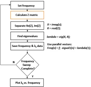
Figure 3.2 Flow chart describing eigenvalues calculation. . . 35
Figure 3.3 Eigenvalues for a 30 cm dipole without DNG sleeve. . . 36
Figure 3.4 Dipole eigenvalues for εr and μr= -1 . . . 36
Figure 3.5 Dipole eigenvalues for εr
=
μ
= -0.6.
. . . 37Figure 4.1 VHF antenna concept . . . 39
Figure 4.2 Effect of height variation on s11. . . 40
Figure 4.3 Effect of slot width on S11. . . 41
Figure 4.4 Smith charts showing slot width impact on S11. . . 42
Figure 4.5 Effect of sheet overlap on S11. . . 43
Figure 4.6 Smith charts showing effect of sheet overlap. . . 44
Figure 4.8 CMA data for VHF antenna. . . 46
Figure 4.9 CMA equivalent circuit. . . 47
Figure 4.10 Current Distribution on VHF Antenna. . . 48
Figure 4.11 First VHF prototype antenna. . . 49
Figure 4.12 VHF antenna balun. . . 50
Figure 4.13 Experimental setup for S11 measurement. . . 50
Figure 4.14 Comparison of measured and simulated S11. . . 51
Figure 4.15 Second VHF prototype. . . 52
Figure 4.16 Model of initial structure. . . 53
Figure 4.17 S11 changes due to structural integration . . . 54
Figure 4.18 Smith charts showing effects of dielectric material. . . 55
Figure 4.19 Effect of foam buffer thickness on S11. . . 56
Figure 4.20 Simulated radiation patterns for structural antenna. . . 57
Figure 4.21 Results for single sweep CMA. . . 58
Figure 4.22 Results for segmented CM analysis. . . 59
Figure 4.23 VHF antenna in sandwich structure. . . 61
Figure 4.24 ECC for UAV with twin vertical tails. . . 63
Figure 4.25 FEKO model of an inverted V tail UAV. . . 63
Figure 4.26 ECC for the inverted V tail model. . . 64
Figure 4.27 Simulated radiation pattern for inverted V tail UAV. . . 65
Figure 5.1 Monoqocue fuselage section with conformal spiral antenna. . . 69
Figure 5.3 Impact of bulkhead position on simulated gain. . . 71
Figure 5.4 Impact of bulkhead position on simulated axial ratio. . . 71
Figure 5.5 Spiral antenna backed by a reflector. . . 72
Figure 5.6 Spiral antenna and simulated S11. . . 73
Figure 5.7 Simulated S11 for various distances between spiral and reflector. . 73
Figure 5.8 Simulated gain for various distances between spiral and reflector. 74 Figure 5.9 Simulated axial ratio for various distances between spiral and reflector. . . 74
Figure 5.10 18 x 18 EBG under spiral antenna. . . 76
Figure 5.11 Simulated S11 for EBG-backed spiral antenna. . . 77
Figure 5.12 Simulated gain for EBG-backed spiral antenna. . . 78
Figure 5.13 Simulated axial ratio for EBG-backed spiral antenna. . . 78
Figure 5.14 Concept for structural integration of EBG and spiral antenna. . . 79
Figure 5.15 Parameters needed to calculate the area of partial circular sector. 82 Figure 5.16 Initial EBG design with outer diameter of 77 cm. . . 83
Figure 5.17 Simulated axial ratio for the circular EBG. . . 84
Figure 5.18 Simulated gain for the circular EBG. . . 84
Figure 5.19 Simulated S11 for the circular EBG. . . 85
Figure 5.20 Revised EBG design with outer diameter of 83 cm. . . 85
Figure 5.21 Metallic wall added below the EBG layer. . . 87
Figure 5.22 Modified EBG with longer center patches. . . 88
Figure 5.23 Pototype EBG. . . 89
Figure 5.25 Prototype EBG structure. . . 91
Figure 5.26 Measured and simulated S11 for the prototype structure. . . 92
Figure 5.27 Measured and simulated axial ratio for the prototype structure. . 92
Figure 5.28 Measured and simulated gain for the prototype structure. . . 93
Figure 5.29 Test cases to study patch length impact on gain roll off. . . 94
Figure 5.30 Simulated gain showing effect of patch length in the outermost row. 95 Figure 5.31 Simulated axial ratio showing effect of patch length in the out-ermost row. . . 96
Figure 5.32 Overhead view of the spiral antenna above the EBG. . . 97
Figure 5.33 Impact of shorted spiral arms on simulated axial ratio. . . 98
Figure 5.34 Impact of shorted spiral arms on simulated gain. . . 98
Figure 5.35 Measured radiation pattern at 520 MHz. . . 99
Figure 5.36 Measured radiation patterns for the UHF prototype. . . 100
Figure 5.37 Measured efficiency. . . 101
Figure 5.38 Fuselage section with EBG assembly installed. . . 101
Chapter 1
Introduction
1.1 Background
Although the use of remotely piloted aircraft and auto piloted vehicles, so called unmanned aerial vehicles (UAV) or drones, started out primarily in military appli-cations, the growth of the commercial drone industry is expected to out pace the military by 14% between 2015 and 2020 [1]. For example, Google and Facebook have purchased aerospace companies with the goal of providing internet access to remote areas via high altitude, long endurance aircraft. Amazon is developing technology to deliver packages to customers using drones, and drone manufacturers are now specifi-cally marketing vehicles for commercial operations[2, 3, 4]. Wireless communications is at the core of all of these applications. The work described in this dissertation deals with enabling not only more efficient antennas for UAVs such as those shown in Figure 1.1, but also more weight efficient ways of incorporating antennas onto the aircraft.
Conventionally, the design of aircraft structures and functional subsystems are considered to be separate areas of endeavor, with the primary aim of this philosophy being to reduce complexity in the design process [7]. In the case of aircraft antennas, the standard manufacturing techniques used for attaching antennas to the vehicle can introduce additional weight, aerodynamic drag, or both. While these issues are detri-mental to performance in any air vehicle, weight and drag are critical considerations in high-altitude, long endurance (HALE) vehicles such as the Solara 50 and weight is an important factor for small drones.
One approach that has been suggested to overcome the problems associated with traditional antenna integration methods is to develop multifunctional air vehicle structures that are capable of performing an antenna function in addition to their conventional role of carrying flight loads [8, 9]. Known in the literature as Confor-mal Load-bearing Antennas Structures (CLAS), this concept is an unconventional approach to aircraft design in which the vehicle’s structure is designed and fabricated with conductive geometry as an inherent part of the structure to enable a desired antenna function. The ultimate goal of this approach is to enable enhanced RF performance while having minimal weight and drag impact on the flight vehicle.
The conventional approach for antenna integration with an air vehicle is to de-sign the antenna as a stand-alone device, and subsequently package the antenna in a protective housing that is then attached to the vehicle. Although simulations can be used to investigate and compensate for some of the effects of the vehicle on antenna performance, the antenna often requires tuning after mounting. Figure 1.2 shows a UHF aircraft antenna packaged in an aerodynamic housing for attachment to the ex-terior of the vehicle. Antennas with this form factor are referred to as blade antennas and are commonly used on commercial aircraft.
Figure 1.2: (a) UHF Blade antenna for aircraft applications [10]. (b) Direct Write VHF antenna on aircraft fairing [11].
[12, 13]. An alternative approach is to leverage the physical space available on an aircraft’s structure to enable a larger antenna. Figure 1.2b illustrates an example of this concept in which a VHF antenna was fabricated on a Boeing 737 fairing using Direct Write technology [11]. This offers the advantage of large antenna with an insignificant weight increase and no drag penalty for the aircraft.
1.2 Objectives
The ultimate goal of this work is to study and design multifunction structures that can be functional blocks of an aircraft such as a vertical stabilizer or fuselage as well as support RF antenna functions for communications and radar. As mentioned, the general topic area falls within the CLAS concept. Chapter 2 provides a more in-depth review of previous work within the CLAS topic area. A brief literature review of CLAS reveals the following notable areas of contributions:
1. Slotted waveguide arrays made within composite structures operating at X-band [14, 15]
3. Structurally Integrated X-band Array [16].
4. Ku-band Microstrip patch antennas and their general adaptation within a com-posite sandwich panel [17].
5. UHF Log Periodic Dipole Array (LPDA) within fiberglass composite [18].
6. Pixelated reconfigurable L-band patch antennas using MEMS [19, 20].
As can be seen in the works outlined above, there is a significant gap in terms of CLAS antenna research in the VHF and UHF frequency ranges. To our knowledge, no work in the VHF frequency range has been reported for composite aircrafts. To note that Characteristic Mode Analyses (CMA) can be a valuable tool for the study of efficient VHF antennas and structures because it can analyze and predict the radiating modes of a structure without any attribution or knowledge to the excitation. This may allow the design of more efficient antennas that can allow broad bandwidths with the help of modal interactions. However, except for the CMA of a bolt-on antenna on a UAV [21] there has been no study reported on a truly structural VHF antenna. Secondly, when it comes to UHF antennas the published work on UHF LPDA within a composite structure focuses on an endfire array only [18]. There is a tremendous need to design and develop structurally integrated antennas that can offer circular polarization with very small cavity depth to ensure low profile and lightweight aircraft. While the VHF concept to be investigated is relevant to VHF communications, SIGINT, and radar, the UHF concept to be studied is relevant to satellite systems such as UHF SATCOM and MUOS.
of the antenna cavity by at least 50%. The primary focus will be on antennas that can be functional and integral to a composite structural panel constrained by the geometrical shapes and materials that are being used in composite aircraft.
1.3 Outline
This dissertation is organized into six chapters. In chapter two, a brief outline on the theory of characteristic modes is presented and terminology relevant to the research presented here is discussed. Chapter two also contains a literature review that covers previous CMA and CLAS research. Chapter three reviews work on the application of CMA to a dipole coated with a sleeve of DNG material. In this work, a MATLAB script was developed to conduct modal analysis first on a dipole of 0.75 mm radius, and then on the same dipole coated with a 0.5 mm thick layer of DNG material. The commercial software FEKO was used to provide corroborating data. Chapter four covers the development of a novel broadband VHF antenna for airfoil integra-tion. The parametric study used to develop and optimize the antenna geometry is discussed, and a method of integrating the antenna with a composite structure is pre-sented. The chapter concludes with a feasibility assessment of a MIMO application based on two such multi-function airfoils. Chapter five reviews the development of a structural EBG to enable a directional, circularly polarized antenna to be integrated with a composite structure. The development of the EBG is discussed followed by the fabrication details for a prototype structure that contains the EBG and a spiral antenna. Results of S11 and anechoic chamber tests are then compared to simulated
Chapter 2
Background
Garbacz first proposed the theory of characteristic modes in 1968 [22]. Shortly there-after, Garbacz and Turpin published a paper that discussed a technique for finding characteristic mode currents on wires of small diameter having a general shape [23]. The approach described in that work involved an analysis of the scattering matrix of a conducting body, specifically the diagonalizing of the matrix. Harrington and Mautz subsequently offered an alternative approach by proposing that characteristic modes could also be determined from the generalized impedance matrix of the conducting body [24, 25]. This approach has garnered much attention because Method of Mo-ments codes provide access to the impedance matrix. While a thorough description of characteristic mode theory can be found in the aforementioned works, a summary of the theoretical work of Harrington and Mautz is provided here.
2.1 Theory of Characteristic Modes
Figure 2.1 depicts a physical scenario that assists in understanding the computation of characteristic modes. An electric field, E~
a, is applied to a conductive surface,
S. An equation that relates the surface current, J~, on S to the tangential electric
field can be defined through the use of a linear operator as in Equation 2.1, where the subscript refers to the tangential components on the surface. The operator L is defined as shown in Equations 2.2 - 2.5, where r indicates a field point, r0 denotes
a point on the source, and ε, μ, and k, represent the permittivity, permeability, and
Figure 2.1: Conductive surface and coordinate system for calculation of characteristic modes.
|L(J~)−E~a|tan = 0 (2.1)
L(J~) = jωA(J~) +∇Φ(J~) (2.2)
A(J~) = µ ‹
S
~
J(r0)ψ(r, r0) ds0 (2.3)
Φ(J~) = − 1
jω ‹
S
∇0·J~(r0)ψ(r, r0) ds0 (2.4)
ψ(r, r0) = e
−jk|r−r0|
4π|r −r0| (2.5)
From a physical perspective, the electric field intensity, E~, at any point in space
Fur-thermore, the linear operator, L, in Equation 2.2 has the units of impedance and can thus be expressed as shown in Equation 2.6.
Z(J) = [L(j)]tan (2.6)
Harrington and Mautz point out that the impedance operator is complex and can thus be expressed as in Equation 2.7 [24].
Z(J~) = R(J~) +jX(J~) (2.7)
Harrington and Mautz further state that the characteristic current modes can be determined as the eigenfunctions of a particular weighted eigenvalue equation of the form shown in Equation 2.8 and showed through additional work that such an equa-tion can be solved by reducing it to matrix form using Galerkin formulaequa-tion, as shown in Equation 2.9 [25].
X(J~n) = λnR(J~n) (2.8)
[X]J~n = λn[R]J~n (2.9)
Characteristic modes are real surface currents on a conducting body that can produce a radiated field. These currents are entirely dependent on the shape and make-up of the body and are independent of excitation. The remainder of this chapter deals with salient terminology related to characteristic modes.
2.2 Eigenvalues
For each characteristic mode, there is an associated eigenvalue, sometimes referred to as a characteristic number, which conveys important information about the mode itself. To illustrate this, the first three eigenvalues for a 750 MHz, thin wire, half-wave dipole antenna are calculated and plotted versus frequency in Figure 2.2. In general, the magnitude of the eigenvalue, |λn |, is a figure of merit that indicates how well a
given mode radiates. Modes for which |λn | is small are the most effective radiators,
while large values of |λn | indicate that a mode is a poor radiator [26]. Resonance is
indicated when the value ofλn is zero. The sign ofλn also conveys information about
how a particular mode tends to store energy. Magnetic energy storage is indicated by positive eigenvalues, while electric energy storage is indicated by negative eigenvalues [27]. Thus, as seen in Figure 2.2, the first eigenvalue is zero at 750 MHz, indicating resonance, and the two higher order modes have large negative values. The latter condition indicates that the modes in question contribute little to the radiated power and act in a capacitive manner (i.e. storing electric energy). Furthermore, all of the modes take on positive values after the zero crossing, indicating inductive behavior.
2.3 Modal Significance
Figure 2.2: First three eigenvalues for a 20 cm, 750MHz half-wave dipole antenna with 1 mm diameter.
M S =
1
1 +jλn
(2.10)
Modal significance is an inherent property of a mode that indicates the degree to which the mode can couple with an external source. Figure 2.3 shows a modal significance plot that was created using Equation 2.10 and calculated eigenvalue data for a 33.3 cm, 450 MHz half-wave dipole antenna having a radius of 1 mm. For the resonant conditionλn= 0, the modal significance achieves its maximum value of one,
making the resonant frequencies easy to locate on the plot. The concept of modal half-power bandwidth is also indicated in Figure 2.3. By considering the frequencies at which the modal significance reaches the half power point, defined as in Equation 2.11, the modal half-power bandwidth is defined as shown in Equation 2.12, where fu
and fl are the upper and lower frequencies at which the modal significance is 0.7, fr
is the resonant frequency (where MS = 1), and the subscript n denotes the nth mode.
M S =
1
1 +jλn
= √1
2 ≈0.707 (2.11)
BWn =
fu −fl
Figure 2.3: Modal Significance for a 450 MHz Dipole Antenna.
A useful application of modal significance is to determine which characteristic modes are significant in terms of contributing to radiated power. A mode is considered significant when M S ≥ 1/√2 while the case of M S < 1/√2 indicates a
non-significant mode [29].
2.4 Characteristic Angle
The theory of characteristic modes states that a conducting body can support a set of real characteristic currents that each give rise to a radiated characteristic field
~
En. The tangential component of the characteristic field is equiphase at all points
on the conductive body and there is consequently a phase lag between the surface currents and the tangential field component. This phase lag can be calculated using the eigenvalues and Equation 2.13 whereαn denotes the phase angle, which is referred
to as the characteristic angle. Figure 2.4 shows an example of a characteristic angle plot that was created using the calculated eigenvalue data from Figure 2.2. The characteristic angle can be used to determine a resonant state, which occurs when
λn = 0, and it indicates that the characteristic surface current is 180° out of phase
with the tangential component of the radiated field. For the case of the tangential field component and modal surface current being 90° or 270° (αn = 90° and αn
= 270°), the mode is in a condition known as internal resonance and this results in minimal radiated power. The characteristic angle can also indicate the nature of energy storage; with inductive energy storage indicated byαnhaving a value between
90° and 180°, and a capacitive mode being indicated when the value of αn is in the
range of 180° and 270° [29].
αn = 180°−tan−1λn (2.13)
2.5 CMA Literature
One innovation being proposed in this research is the application of CMA in the study and development of CLAS concepts. Because this represents an intersection of two previously unrelated concepts, CMA and CLAS literature will be reviewed in the following two sections. The two topics are then brought together in Chapter 4 where
CMA is applied in the development of an airfoil-integrated VHF antenna.
Adams and Bernard investigated the use of CMA to analyze an electrically small antenna with emphasis on antenna tuning and bandwidth enhancement through modal techniques [30]. Figure 2.5 shows the antenna geometry, which is a four-arm TM10 monopole. The antenna consists of four dielectric arms of constant radius
that are oriented in theφ= 0° andφ= 90° planes to support helical wires coiled along
their length. This structure is bisected in the θ= 90° by a substrate containing a
ground plane on the bottom and traces connected to the base of each wire coil on the top. The antenna is fed from the bottom and connects to the intersection of the two traces.
CMA was conducted on the geometry, and the first and second modal currents and their associated characteristic angles are shown in Figure 2.6a and b, respectively. As can be seen on the left of the figure, there is more current in the spherical arms than in the traces for mode 1, but this condition is essentially reversed for mode 2 which has significantly more current in the traces. The characteristic angle plots show that both modes are initially capacitive and mode 1 goes through resonance at 850 MHz and becomes inductive. Mode 2 remains capacitive and ultimately resonates at 1.57 GHz before going inductive. As indicated by the slope of its characteristic angle plot, mode 1 has the lower eigenvalue magnitude over the band of operation and thus provides most of the antenna’s radiation. Mode 2 provides capacitive admittance in the antenna’s operating band.
Figure 2.6: (a) Characteristic currents for modes 1 and 2 (b) Characteristic angle plots for modes 1 and 2 [30].
Figure 2.7: Circuit model for antenna input impedance from a CMA perspective [30].
Yin=
X
n
Jn2
1 +λ2
n
(1−λn) (2.14)
The use of CMA to study the optimum location to place an antenna on an air vehicle was studied by Chalas [31]. The antenna in this case is considered more of a probe to excite currents on the surface of the aircraft which give rise to radiated fields. This is a concept that was first proposed by Newman [26].
The operation of a general coupled antenna-platform system can be expressed using the Method of Moments (MoM) as in Equation 2.15. In this expression, [ZAA
]
and [ZPP]
represent the impedance matrices of the antenna and vehicle, and [ZAP]
and [ZPA]
are the antenna-vehicle mutual coupling matrices. Also IA and IP are the currents on the antenna and vehicle, and VA and VP are the antenna and vehicle voltages.[Z]{I} =
[ZAA] [ZAP]
[ZP A] [ZP P]
{I}A
{I}P
=
{V}A
{V}P
(2.15)
Figure 2.8: First four eigenvalues and characteristic currents for UAV model [31].
modal decomposition on the impedance matrix of the vehicle, [ZPP
]
. The frequency of interest for the study was 11.5 MHz, and Figure 2.8 shows the modal currents and associated eigenvalues for the first four modes supported by the vehicle. The eigenval-ues indicate that modes one and two, being close to zero, can radiate efficiently, while the larger eigenvalues for modes three and four indicate these modes more reactive in nature - especially in the case of mode four.The coupling between the antenna and vehicle was then investigated by assuming that an electrically small, inverted L antenna (ILA) was to be placed somewhere along the top of the fuselage and the location was varied while observing the effects on the 3 dB bandwidth of the ILA. Figure 2.9 shows the results of the analysis, with the x-axis denoting the ILA location expressed as a ratio of position to overall fuselage length, x/L. As indicated by the plot, the bandwidth is larger when the antenna is located near the tail and reaches a minimum value when the antenna is positioned at the midpoint of the fuselage. Thus a strategic choice of antenna location results in increased bandwidth.
Figure 2.9: Matched 3 dB fractional bandwidth seen at the antenna input when mounted on UAV[31].
versus antenna location, which is once again expressed as the ratio of x/L. The plot clearly shows that the most power is radiated by the first mode when the ILA is near the tail where coupling is maximized. As the ILA is moved toward the center of the fuselage, coupling to the vehicle and radiated power decrease, and only the antenna radiates when positioned at the midpoint of the fuselage. As the ILA is moved toward the front of the vehicle, coupling to modes one and three increases, and there is an associated increase in radiated power.
Figure 2.10: Power radiated by each of the first four vehicle characteristic modes as a function of location on fuselage [31].
Figure 2.11: Laboratory model of a metallic air vehicle [21].
be directed upward, to the front, and to the rear.
Figure 2.12: Characteristic currents and fields for a) mode 1, b) mode 2, c) mode 3, d) mode 4 [21].
manipulates modal coefficients to synthesize surface currents and radiated fields and seeks convergence between these quantities and objective functions derived from the design goals and input data. The output of the optimization software is a set of synthesized current and field solutions from which a particular solution can be selected manually. Figure 2.13 show the results of the optimization process, with real and imaginary currents shown on the surface of the aircraft and the resulting radiated fields for each case. It is interesting to note that the current excitation required to produce the forward and rearward beams differ only by a 180° phase reversal of the imaginary current.
To enable experimental validation of the simulated results, two antennas, a slot monopole and inverted F, were designed and are shown in Figure 2.14a and b. It is important to note that these antennas were optimized for use as probes to excite the surface currents shown in Figure 2.13, and S11 was on the order of -5 dB when
Figure 2.13: Synthesized real (right) and imaginary (left) currents and radiated fields resulting from the optimization process [21].
Figure 2.14: a) Slot monopole antenna. b) Inverted F antenna [21].
slot monopoles were attached to the wing of the vehicle model such that the ground plane was shorted to the wing, as seen in Figure 2.11, and the inverted F probe was attached to the tail of the model.
Figure 2.15: Measured data (a) 3dB upward (b) 0.14 dB forward (c) 5 dB rearward [21].
2.6 CLAS Literature
The first project that investigated the concept of load-bearing antennas was the Smart Skin Structures Technology Demonstration (S3TD) [8, 9]. The goal was to integrate a multi-use antenna into a composite panel that could take loads typical of those seen by the fuselage of a fighter aircraft, as indicated in Figure 2.16, and a cross sectional view of the structural antenna concept is shown in Figure 2.17.
A section of core material is located below the dielectric layer to provide structural stiffness in conjunction with the inner and outer face sheets. One significant feature of this assembly is the attachment of a non-structural, RF absorber behind the antenna to absorb fields radiated inward. While necessary for RF performance, the absorber and the housing that contains it represent parasitic weight. An alternative to this approach will be explored in Chapter 5. The S3TD program culminated with the successful testing of a 36 by 36 inch antenna panel that withstood strain levels of 4,000 microstrain and loads up to 148,000 kips as well as a buckling load of 4,000 pounds per inch. The panel survived 6,000 hours of fatigue testing and was subsequently tested to ultimate failure which occurred at 150% of design limit load.
In the Structurally Integrated X-band Array (SIXA) project, an effort was un-dertaken by Boeing and Raytheon to develop a large scale wing component that contained an X band array [16]. The concept was based on a composite sandwich structure in which the walls of an egg crate-shaped core (Figure 2.18a) hosted antenna elements. It should be noted that the core shape represents a trade-off between elec-trical and mechanical performance. A honeycomb shape provides optimal structural
Figure 2.17: Cross-sectional view of S3TD assembly [8].
Figure 2.18: (a) Egg crate core section and unit cell depicting antenna elements (b) 3 point bending test of structural coupon [16].
performance, but the egg crate shape enabled a dual polarized array as is shown on the unit cell in Figure 2.18a.
Figure 2.19: RF electronics are mounted on the inside of the structure [16].
withstanding high strain, temperature fluctuations, and mechanical fatigue.
Figure 2.20: Wing box assembly mounted in a test rig [16].
Figure 2.21: Antenna concept for structural integration [17].
Another approach for integrating an antenna with a composite structure was investigated by You et al. [17]. This work also incorporated a sandwich structure and was aimed at addressing the trade-off between electrical and structural performance. Figure 2.21 shows a stacked microstrip patch antenna concept that was considered for integration. The antenna is fabricated using Rogers Duroid 5880 boards that are typically used for RF circuitry and antennas. A unique feature in this case is the use of a 2.54 mm thick layer of Nomex honeycomb core material typically used in composite structures to separate the two patch layers.
Figure 2.22: Integration of antenna into sandwich structure [17].
Figure 2.23: Comparison of gain of antenna alone versus structural antenna [17].
of the sandwich structure and the thickness of the upper skin were sized to enhance the electrical performance, and the effect of this approach can be seen in Figure 2.10. The dashed line in the figure indicates that the antenna alone had a peak gain of about 7.5 dBi and a half power beam width of approximately 100°. However, as indicated by the solid line, when the antenna is included in the composite structure, the beam is much more focused and the peak gain approaches 12 dBi.
of structural composite materials to enhance RF performance, it should be pointed out that the structure was sized solely to achieve improved RF performance. No indication was given in this work that mechanical loads of a specific vehicle or class of vehicles were taken into consideration.
Another CLAS concept based on a sandwich structure is the reconfigurable Yagi-Uda developed by Wright et al. [32]. The antenna in this case is formed using an array of metallic pixels as seen in Figure 2.24. A unique feature of this structure is that the metallic elements were created on a polyimide film using ink jet direct write technology. The film was then bonded to the surface of the sandwich structure. In theory, a number of different antenna geometries can be created by interconnecting the pixels with RF MEMS switches. However, this work considered the case of a driven dipole element at the center of the pixel field with switchable reflectors on either side of the driven element. This arrangement is depicted in the inset on the upper left side of the figure. Directors were located in the pixel field outside of each switchable reflector and were made by permanently connecting columns of pixels at the appropriate distance.
The concept of operation is that only the switches on one side of the driven element are active at any time (thus forming a reflector) and the opposite switched structure (with switches off) acts as a director. RF energy can be directed to the left by engaging the switches in the reflector on the right and vice versa. Because a ground plane was included in the lower skin of the sandwich structure, the beam will project at a 45° angle from the surface of the structure.
The measured pattern data at the bottom of Figure 2.24 shows that the antenna structure worked as designed, but the measured S11 data on the left shows that the
Figure 2.24: Reconfigurable Yagi-Uda antenna in sandwich structure [32].
incorporating RF MEMS switches into a mechanical structure.
Another example of the use of a composite structure to host an integrated antenna was investigated by Bishop [18] et al., and the concept is illustrated in Figure 2.25. The desired RF performance in this case was a linearly polarized directed beam with a bandwidth of over two octaves beginning at 350 MHz and a gain of 6 dBi or more across the band. One significant structural difference in this work was the use of Kevlar to fabricate the dielectric surfaces as opposed to fiberglass used in the previously described research. Kevlar is advantageous from an RF perspective being lower loss than fiberglass (εr= 3.85, tanδ= 0.008 at 10 GHz), but can be problematic
arms on the lower surface. An important fabrication detail is that the connections were made with conductive epoxy which accounted for bending or flexing of the structure under mechanical loading. At the narrow end of the array, the center conductor of the coaxial cable was connected to the metallic tube to complete the feed assembly, as shown in the lower portion of Figure 2.25. It should also be noted that a meander line approach was used for the dipole arms to meet space constrained applications such as found on small UAVs.
A prototype of the antenna was fabricated to assess performance of the feed assembly and manufacturing techniques. A photo of the prototype is shown in the inset in Figure 2.26. Of critical concern was maintaining a 3 mm gap between the coaxial cable and feed tube over the length of the array. This was accomplished using 3-D printed spacers that are visible in the photograph. After assessment of the prototype was completed, a structural version was fabricated and subjected to both Mechanical and RF testing. The measured VSWR and gain are shown in the plots on the left and right side of Figure 2.26, respectively. As seen on the plots, the maximum VSWR is 3 around 480 MHz and the gain is 7 dB or more over most of the band.
Finally, the use of a structural stiffener as a slotted waveguide antenna has also been explored by the Australian Defense Science and Technology Orgainsation (DSTO) [33, 15]. Stiffeners are common structural features in aircraft, and Figure 2.27a illustrates one example of a stiffened composite panel which is representative of a hatch cover. The concept is to match the dimensions of the stiffener to those of a standard waveguide, such as the WR-90 investigated by the DSTO. The appeal of this approach is that there is no additional hardware needed because the stiffener provides both a mechanical and electrical function, and there is consequently little, if any, parasitic weight.
Figure 2.25: Log periodic dipole array hosted in a composite sandwich structure [18].
Figure 2.26: Measured VSWR (left) and gain (right) for the structural antenna; prototype in inset [18].
Figure 2.27: a. Stiffened composite panel. b. Stiffened composite panel with various radiating slots. [33].
Chapter 3
CMA analysis on a Dipole Antenna Loaded with
DNG Material
3.1 Theoretical Approach
While commercial software packages such as FEKO now offer the ability to conduct CMA on complex geometries and materials (which we will do in a subsequent chap-ter), such an approach does not enable an understanding of the analysis method itself. For that reason, a theoretical study of a half-wave dipole was undertaken to under-stand the physics of the method and how it works. Previous work by Cabedo [34] covered the application of CMA to a conventional dipole, so this work focused in-stead on a DNG loaded dipole. Although the study of the impedance response by DNG material loading on a dipole antenna was proposed by Shams and Ali [35], the application of CMA to a DNG loaded dipole is new and thus extends the previous work by Shams and Ali. Specifically, our eigenvalue study sheds new light in terms of its prospects of antenna size miniaturization if DNG materials become available.
The geometry considered in our investigation is depicted in Figure 3.1. The overall length, L, is 30 cm, the wire radius is 0.75 mm, and the DNG material is 0.5 mm thick; thus, the diameter of the wire/sleeve structure is 2.5 mm. The DNG material is assumed to be isotropic and homogeneous.
an-Figure 3.1: Dipole antenna with sleeve of DNG material.
tenna structure, to form what could be viewed as an array of smaller dipoles. The impedance matrix was then found using Equations (3.1) to (3.5) by first calculating the impedance matrix of the dipole in free space (given by Equation 3.1), calculating the effects of material loading using Equations (3.2) to (3.5) (where F0
m
(z)
and F0
n
(z)
are the Piecewise Sinusoidal (PWS) basis functions indicated in Figure 3.1, ais the radius of the wire making the dipole, and b is the wire radius plus the coat-ing thickness), and finally calculatcoat-ing the first row of the impedance matrix as given by Equation 3.6. The complete matrix can then be populated using the Toeplitz algorithm, which can easily be accomplished by applying the toeplitz() function in MATLAB.
Zd = −
"Z zn2
zn1
sinβ(z−zn1)
sin(β∆) +
Z zn3
zn2
sinβ(zn3 −z)
sin(β∆)
#
j30
sin(β∆)
×
"
e−jβRm1
Rm1
−2 cos(β∆)e
−jβRm2
Rm2
+ e
−jβRm3
Rm3
#
dz (3.1)
Ze =−
P
2πjω0
Z
Fm0 (z)Fn0(z)dz (3.2)
Zm = Q
jωµ0
2π
Z
P = 2 −1 2 ln b a ! (3.4)
Q = (µr −1) ln
b
a
!
(3.5)
Z1 =Zd +Ze+Zm (3.6)
3.2 Results of CMA
As pointed out in the previous work by Cabedo[34], MATLAB provides a convenient method to calculate both eigenvalues and eigencurrents through use of theeig() func-tion. As depicted in the flow chart of Figure 3.2, this feature can be used to create a plot of eigenvalues versus frequency by implementing a nested-loop script that first calculates the impedance matrix and then calls the eig() function to calculate the eigenvalues for that frequency. The highlighted processing block in Figure 3.2 is the impedance matrix calculation described above, and it comprises the inner loop of the script. The impedance matrix must be re-calculated at each frequency because it is frequency dependent. By storing the eigenvalue and frequency data as parallel arrays, it is straightforward to create eigenvalue plots that can be used to determine the resonant frequency of each mode by locating the points at which the eigenvalues cross zero.
Figure 3.2: Flow chart describing eigenvalue calculation.
studies were also conducted (but not reported here) where other positive values of εr and μr were considered.
Figure 3.3: Eigenvalues for a 30 cm dipole having a diameter of 1.5 mm and no DNG sleeve.
Figure 3.4: Eigenvalues for a 30 cm dipole having a 1.5 mm diameter and a 0.5 mm thick DNG sleeve withεr and
μr= -1
Figure 3.5: Eigenvalues for a 30 cm dipole having a 1.5 mm diameter and a 0.5 mm thick DNG sleeve withεr
=
μ
r= -0.6.
Table 3.1: Effect of a 0.5 mm thick DNG sleeve on the resonant frequency of a 30 cm long dipole antenna having a diameter of 1.5 mm.
εr
,
μ
r Res. Fr. (MHz) εr,
μ
r Res. Fr. (MHz)-0.3 355 -0.7 442
-0.4 392 -0.8 451
-0.5 415 -0.9 459
Chapter 4
Airfoil-integrated VHF Antenna for MIMO
Applications
VHF antennas are very important for air-to-ground voice and data communications [36] as well as SIGINT, COMINT, and radar [37]. VHF antennas are also widely used in military land vehicles [38] and shipboard applications. More recently they are being considered for cognitive radio communications and airborne internet service for remote and sparsely populated areas.
Conventional VHF aircraft antennas, such as blade antennas, are electrically small. In order to obtain sufficient bandwidth these antennas are resistively matched which results in very low efficiency. Gain of -20 or -30 dBi at the lower VHF frequen-cies is fairly common. Additionally, these antennas are usually externally mounted on the aircraft i.e., they protrude from the surface of the aircraft. As a consequence, aerodynamic efficiency is also reduced. While antennas such as annular slots could solve this problem, they have a narrow bandwidth.
Figure 4.1: (a) Airfoil (b) Antenna geometry.
pattern are considered as performance goals. The choice of this frequency range is simply due to the number of applications in this range such as aircraft air-to-air and air-to-ground communication, RF navigation equipment, emergency locater beacons, marine radio for maritime search and rescue, military ISR and communications, and cognitive radio.
4.1 Antenna Development
Figure 4.2: Effect of height variation on s11.
cm was assumed.
Antenna analyses and design were performed using FEKO. Figure 4.2 shows how variation in the vertical separation between the two conductive sheets affects the S11
performance. Two observations can be made from the plot. The first is that for e = 2.5 cm, a sharp resonance is seen at 185 MHz which agrees well with the resonant frequency of 187.5MHz for a 40 cm monopole. Secondly, it can be seen that the bandwidth increases and frequency of operation shifts lower as the distance between the sheets increases. An initial distance of 3.5 cm was selected because a lower height facilitates integration with an airfoil. The bandwidth within S11 < -10 dB is 120 to
200 MHz.
Figure 4.3: Effect of slot width on S11.
the effects of adding a slot next to them were studied.
The location and geometry of the slot can be seen from Figure 4.1d. The impact of the slot was investigated by observing the effect on S11 while varying the slot depth
(g) in 2 cm increments from 2 cm to 14 cm, and Figure 4.3 shows the data resulting from the simulations. The data show that a narrower slot contributes to bandwidth at lower frequencies while a wider slot increases bandwidth at higher frequencies. The sharp resonance at the high frequencies was determined to be caused by the stubs by repeating the simulation with stubs removed. A key observation is that a 12 cm slot depth provides the upper portion of the desired bandwidth, from 160 MHz to 224 MHz, and also a small segment at the low end of the band from 90 MHz to 106 MHz. Thus, the antenna would meet the desired impedance bandwidth if the match could be improved between 106 MHz and 160 MHz. The effect of the slot was also studied with a Smith chart, with the results shown in Figure 4.4.
Figure 4.4: Smith charts for slot widths of (a) 2 cm (b) 6 cm and (c) 12 cm.
to control the equivalent shunt capacitance resulting from the sheet overlap, which is in parallel with the feed. Figure 4.5 shows the effect on S11 when the amount of
overlap between the sheets is increased. As the plot shows, once the overlap reaches 8 cm, the S11is below -10 dB from approximately 95 MHz to 235 MHz. Thus a 2.5:1
bandwidth is achieved. The effect of the overhang was also studied with the Smith chart, and the plots in Figure 4.6 show the results. A shift downward can be seen on the plots as overlap increases, as would be expected for increased capacitance due to a larger overlap area.
Figure 4.5: Effect of sheet overlap on S11.
practice in industry to specify parameters under the best case conditions on data sheets. Thus, it is reasonable to expect that the antenna developed in this section would perform similarly to commercial products, and that RF systems utilizing this antenna would be able to function across the entire band despite the dips in the pattern at higher frequencies.
Table 4.1: Dimensions of the pro-posed antenna.
Parameter cm Parameter cm
a 62 f 58
b 76 g 12
c 40 h 8
d 22 i 14
e 3.5 j 6
4.2 Characteristic Mode Analysis
Figure 4.7: Radiation patterns at φ= 0, φ= 90,θ= 90 for 97 MHz (top) and 240
MHz (bottom).
frequencies becomes a potential problem when conducting modal analysis because a much finer mesh size is required, and this directly impacts both simulation time and memory usage. Altair’s technical support staff for FEKO recommends mesh sizes in the range of λ/20 to λ/25. For the antenna under consideration, the upper
frequency of 240 MHz implies a mesh size of 5 cm using the λ/25 constraint. An
initial simulation was conducted from 80 to 250 MHz using a mesh with a 5 cm edge length, but a number of mode tracking errors were encountered. These errors result when the software loses track of a mode during the simulation and begins logging data of a previously detected mode under a new mode number, giving the appearance of more modes being present. FEKO detects this condition and issues a warning calling for a finer mesh size. It was determined through experimentation that λ/30 to λ/35
Figure 4.8: (a) Modal significance and (b) Characteristic angle for VHF antenna.
96 GB of RAM, the simulation took approximately 24 hours to complete because of the small mesh size.
Figure 4.8 shows the results of the FEKO simulation with modal significance shown on the left and characteristic angle on the right. Using the modal significance plot and recalling that a mode is considered significant for a value equal to or greater than 0.7, it is evident that there are three significant modes (modes 1, 2, and 4) and one non-resonant mode (mode 3) for the VHF antenna. Another observation that can be made is that mode 2 has a very broad bandwidth of 110 MHz, and mode 4 has roughly half that amount at 60 MHz. One interesting aspect of the modal significance plot is that there are no significant modes between 115 and 150 MHz; yet the S11
plot for the antenna in Figure 4.5 (solid blue line) shows the match is good over this frequency band. It would initially seem that there should be another dominant mode over this frequency range.
Figure 4.9: Antenna equivalent circuit from CMA perspective.
capacitive, go through resonance, and then become inductive, while mode 3 remains inductive over the entire band of operation. This observation can be used to construct the equivalent circuit model of Figure 4.9 where each mode is modeled as an arm of a parallel RLC circuit. As seen in Figure 4.8b, inductive mode 3 and capacitive mode 4 are essentially equal and opposite over the band in question, acting to cancel each other. Mode 1 dominates below 100 MHz and then goes inductive in a manner that acts to cancel the capacitive nature of mode 2. Thus the interaction of the modes acts to create a matching circuit.
The current distribution on the antenna was also studied with FEKO. Figure 4.10 shows the current distribution at four different points within the frequency band over which S11 is below -10 dB. The light and dark blue coloration indicates regions of
Figure 4.10: Current distribution for (a) 96 MHz (b) 142 MHz (c) 190 MHz (d) 238 MHz.
4.3 Prototype Antenna
Figure 4.11: Prototype of the VHF antenna.
At the feed point, a section of foam between the sheets was removed, and a PCB containing an RF balun from RF Micro Devices (part no. RFXF9503) was positioned between upper and lower plates. The PCB, shown in Figure 4.12a, has a 50 ohm microstrip at the input (left side of Figure 4.12a), and two traces on the output side to attach wires for connection to the copper sheets. A coaxial cable was soldered directly to the PCB input and the opposite end of the cable was terminated with an SMA connector. The PCB is 3.5 cm wide, and is installed vertically between the two copper sheets to minimize wire lead length. Wires with a diameter of 0.9 mm were soldered to each terminal, and the wires were in turn soldered to the copper sheets at the feed point. A close-up of the balun itself can be seen in Figure 4.12b.
Upon completing assembly of the antenna, an S11measurement was taken. Given
the VHF operating range of the antenna, the S11 measurement was made in a large
Figure 4.12: (a) RF balun mounted on PCB (b) Closeup of chip balun [41].
Figure 4.13: Experimental setup for S11 measurement.
and simulated data can be seen in Figure 4.14.
As seen in Figure 4.14, there is close agreement between the measured and sim-ulated data. The measured S11 was below -10 dB from 93 MHz to 230 MHz, for a
Figure 4.14: Comparison of measured and simulated S11.
used in the simulation than was available when the prototype was constructed, and the smaller 0.9 mm wire and thin PCB trace used to feed the prototype could have caused this reduction in bandwidth.
in the close-up on the upper right, which shows the area around the feed. The same PCB that was used on the first prototype was used for the mesh version and is shown on the upper left of Figure 4.15. The S11 measurement was repeated, and the results
are shown by the blue line in Figure 4.14. It was found that mesh antenna had a slightly higher bandwidth ratio (2.5:1) than the first prototype (2.47:1). This came about because the first prototype was inadvertently fabricated with 5 mm less vertical spacing between the upper and lower traces.
Figure 4.15: VHF prototype with expanded metal.
4.4 Basic Structural Effects
x 0.62 m antenna. The initial distance between the dielectric layers was taken as 14.5 cm. The dielectric layers themselves were modeled as 1.5 m x 1 m fiberglass composite sheets with a thickness of 5 mm. The structural model is shown in Figure 4.16 with the dielectric skins shown in blue.
The initial integration scheme was to attach the large slotted sheet of the antenna to the inner side of the lower dielectric sheet, as seen in Figure 4.16. A 3.5 cm layer of foam would be placed on top of this assembly, and the small rectangular sheet would be positioned on top of this foam layer. Another 11 cm foam layer would be then added to achieve the desired 14.5 separation distance followed by the upper dielectric sheet. The feed was modeled with 5 mm diameter wire with a voltage source located at the center point. The dielectric properties of the fiberglass panels were taken to be εr= 4.0 with tanδ= 0.01, and the foam was modeled as air (εr= 1), although, as previously mentioned, some of the more dense foams used in structural composites can be slightly higher with εr= 1.08.
The results of the FEKO simulation for the pseudo-structural antenna are shown by the black trace on the S11 plot in Figure 4.17. For comparison, the red trace on
the same graph shows the baseline simulated S11 plot for the antenna in air as
pre-sented in Figure 4.14. It is obvious from comparing the S11 plots that the presence of
the structural material has significantly degraded antenna performance. To examine the variability in dielectric constant and its effect on antenna performance, a second simulation was performed by replacing the fiberglass skins with cyanate-ester/quartz
Figure 4.17: S11 changes due to structural integration.
(εr= 3.25, tanδ = 0.006) to determine the extent to which material properties
con-tributed to the degradation. Interestingly, the results were the same as for fiberglass. This seemed to indicate a problem with the integration scheme itself.
The integration concept was reconsidered, and it was noted that the only major difference between the structural and non-structural antenna was that the lower di-electric sheet was in direct contact with the slotted conductive trace in the structural version. The dielectric sheet was moved downward 5 mm (see Figure 4.16) in the FEKO model to determine if the mere presence of dielectric material near the feed and slot area was affecting the input impedance of the antenna. This 5 mm of sepa-ration could be achieved in a composite structure by adding an additional foam layer between the lower sheet and the slotted trace.
As indicated by the blue line on the S11plot of Figure 4.14, a significant portion of
Figure 4.18: Smith charts showing effects of dielectric material.
Figure 4.18 shows the structural interaction discussed above on a Smith chart. Figure 4.18a is the baseline antenna in air, and Figure 4.18b shows the deleterious effect of the dielectric skin being in direct contact with the slotted rectangular sheet of the antenna. The Smith chart of Figure 4.18c shows that the inclusion of the foam buffer results in much improved performance that is similar to that observed for the baseline antenna.
The effect of the foam buffer thickness on S11 was investigated through additional
Figure 4.19: Effect of foam buffer thickness on S11
structure.
Simulated radiation pattern plots are shown in Figure 4.20, and Table 4.2 shows the peak gain at discrete points in the operating band for each of the dielectric materials that were studied. From a comparison of Figure 4.20a - c and Figure 4.7a-c, it is evident that the patterns in each of the principal planes at the lower end of the band are similar. Comparing the patterns at the upper end of the band in Figure 4.20d-f to those in Figure 4.7d-f, it is seen that there is close agreement in the θ =
90 degree plane, but some variation is found in the other planes. This is because the upper end of the band is 210 MHz in Figure 4.20 whereas it is 240 MHz in Figure 4.7.
Table 4.2: Comparison of simulated peak gain for different composite materials (dBi).
Dielectric 100 MHz 150 MHz 200 MHz
None 2.2 2.7 2.7
Cyanate-Ester / Quartz 2.4 2.7 2.7
Figure 4.20: Simulated radiation patterns at φ = 0, φ = 90, and θ = 90
planes respectively, for (a-c) 95 MHz and (d-f) 210 MHz.
4.5 Characteristic Mode Understanding
The CM analysis discussed in section 4.2 was repeated with the dielectric material included in the model. The analysis was conducted in two ways with the first being a single sweep from 80 to 235 MHz, and the second being a segmented approach consisting of three separate simulations over subsets of the operational band. The latter approach was adopted because FEKO indicated that tracking errors occurred during the single sweep analysis.
Figure 4.21: Results for single sweep CMA.
size used for the single sweep analysis was λ/32 at 235 MHz, which is approximately
4 cm.
To address the mode tracking errors, the bandwidth was divided into three seg-ments, 75 to 130 MHz, 129 to 179.5 MHz, and 179.5 to 230 MHz, and a modal analysis was conducted separately for each segment. Care was taken to maintain the same frequency increment of 2.29 MHz for each analysis segment to aid in merging the data from all segments. It was speculated that this segmented approach would enable a finer mesh to be used, if needed, to eliminate the mode tracking errors. The initial mesh selected was a triangle edge length of 3.5 cm, which is λ/37 at 230 MHz
Figure 4.22: Results for segmented CM analysis.
data for the second segment was saved to the spreadsheet, and the last segment was analyzed using the 3 cm mesh size.
Several problems were encountered with the segmented approach. One issue is that the FEKO mode labels were inconsistent between segments; for example, modes 1 and 2 were interchanged between the first and second segment, as were modes 3 and 4. Another problem was the time required to complete an analysis using the 3 cm mesh size, which, for segment two, was over 66 hours. Finally, manual inspection of the data from all segments revealed that some of the mode tracking errors were caused by FEKO starting a new data set for a previously detected mode. Ultimately, this manual inspection process enabled the modes to be pieced together, and two of the so-called errors were actually higher order modes. Figure 4.22 shows the resulting modal significance plot for the segmented analysis, and Table 4.3 lists some of the details such as mesh size and run time recorded during the analysis process.
downward shift at 2.8 MHz, followed by mode 2 with a 17 MHz reduction, and the resonant frequency of mode 4 decreased by 20 MHz. The structural dielectric material also caused a reduction in modal bandwidth with modes 1 and 4 being reduced by 14.5% and mode 2 decreased by 24.3%.
Upon completing the analysis of structural integration effects, a structural antenna was constructed and is shown if Figure 4.23. The fiberglass sheets used for this antenna were 2 mm thick instead of the 5 mm thick fiberglass and cyanate-ester quartz sheets used in the simulations. The thinner sheets were already on-hand, and this change saved the cost of purchasing commercial composite sheets or the supplies
Table 4.3: Metrics observed during segmented analysis.
Frequency Range (MHz) Edge Length (cm) Triangle Count Modes / Track Errors Run Time (hours)
75 - 130 3.5 15,567 4/2 34.6
129 - 179.5 2.2 - - Error
129 - 179.5 3.0 20,897 4/4 66.2
179.5 - 230 3.0 20,897 4/2 57.8
Table 4.4: Effect of structural material on modal resonance.
Mode No DielectricFr (MHz)
Fr
Dielectric (MHz)
1 94.9 92.1
2 208 191
4 204 184
Table 4.5: Effect of structural material on modal bandwidth.
Mode No DielectricBandwidth (MHz)
Bandwidth Dielectric
(MHz)
1 21.4 18.3
2 106.7 80.8


![Fig ur e 2 .9 : Ma t c he d 3s e e n a t t he a nt e nnadBf r a c t io na l ba ndw idt hinput w he n mo unt e d o nUAV[3 1 ].](https://thumb-us.123doks.com/thumbv2/123dok_us/8371827.1384073/33.612.177.436.69.283/fig-ma-nnadbf-ndw-idt-hinput-unt-nuav.webp)
![Fig ur e 2 .1 4 : a ) Slo t mo no po le a nt e nna . b) I nv e r t e d F a nt e nna[2 1 ].](https://thumb-us.123doks.com/thumbv2/123dok_us/8371827.1384073/36.612.178.434.73.317/fig-ur-slo-nt-nna-i-nv-nna.webp)
![Fig ur e 2 .1 5 : Me a s ur e d da t a( a ) 3 dBupw a r d ( b) 0 .1 4dBf o r w a r d ( c ) 5dBr e a r w a r d [2 1 ].](https://thumb-us.123doks.com/thumbv2/123dok_us/8371827.1384073/37.612.113.490.77.337/fig-ur-me-ur-da-dbupw-dbf-dbr.webp)
![Fig ur e 2 .2 6 : Me a s ur e d VSWR( le f t ) a nd g a in ( r ig ht ) f o r t hes t r uc t ur a l a nt e nna ; pr o t o t y pe in ins e t [1 8 ].](https://thumb-us.123doks.com/thumbv2/123dok_us/8371827.1384073/46.612.165.437.67.451/fig-me-vswr-ig-hes-nna-pr-ins.webp)