Abstract
MELAMED, SAMSON LOUIS BENJAMIN. Junction-Level Thermal Analysis of Three Dimensional Integrated Circuits. (Under the direction of Dr. W. Rhett Davis.)
The degraded thermal path of three dimensional integrated circuits (3DICs) makes accurate
thermal analysis at the chip-scale an essential part of the design process. Performing an appropriate
thermal analysis on such circuits requires a model with junction-level fidelity. The computational
burden imposed by such a model is tremendous and requires the creation of new techniques to
efficiently handle the problem. A custom thermal network extractor is introduced to extract models
that consider the full structure of three dimensional integrated circuits, including interconnect. An
application specific solver is developed to simulate the extractor’s thermal networks in a manner
that is three orders of magnitude faster than off-the-shelf circuit simulators. A method for dividing
the thermal response caused by a heat load into a high fidelity “near response” and a lower fidelity
“far response” is developed and used to implement Power Blurring HD, a hierarchical thermal
simulation approach based on Power Blurring, that incorporates the thermal networks and allows
for junction-level accuracy at the full-chip scale with a runtime that is similar to common digital
design tools. Power Blurring HD is estimated to yield three orders of magnitude of improvement in
memory usage and up to six orders of magnitude of improvement in runtime for a 3 mm×3 mm
3-tier circuit modeled with a 0.1µm×0.1µm element size, as compared to directly solving the
full-chip junction-scale thermal network. A method for preparing circuits for thermal measurement
is introduced, and measurement results are presented showing that Power Blurring HD is able to
Copyright 2011 by Samson Louis Benjamin Melamed
Junction-Level Thermal Analysis of Three Dimensional Integrated Circuits
by
Samson Louis Benjamin Melamed
A dissertation submitted to the Graduate Faculty of North Carolina State University
in partial fulfillment of the requirements for the Degree of
Doctor of Philosophy
Electrical Engineering
Raleigh, North Carolina
2011
APPROVED BY:
Dr. Paul D. Franzon Dr. Michael B. Steer
Dr. Donald L. Bitzer Dr. W. Rhett Davis
Dedication
Biography
Samson Melamed was born in Silver Spring, Maryland in 1982. He received the B.S. degree in
Computer Engineering from the University of Maryland, Baltimore County in 2004, and the M.S.
degree in Electrical Engineering from North Carolina State University in 2007. He has been a
Research Assistant at North Carolina State University throughout his stay and has worked on projects
funded by both DARPA and the NSF. His research interests include thermal simulation, thermal
Acknowledgements
I would like to thank my advisor, Dr. Rhett Davis, for believing in my potential, helping me to find
my way, and always encouraging me to run with gazelle-like speed toward the finish line. I would
like to thank Dr. Michael Steer for his help with circuit modeling, Dr. Paul Franzon for his insight on
simplifying thermal models and Dr. Donald Bitzer for always keeping me grounded in the scientific
approach.
I would like to thank my Mom for all of her encouragement, my Aunt Lucy for her support, Dave
Drucker for his encouragement and Jo Ann and John Goertner for their input and support along the
way.
I would like to thank Thor Thorolfsson for the SAR design and his help as I prepared this
dissertation, Adi Srinivasan and Edmund Cheng for performing simulations in Gradient
HeatWave-3DIC and helping me to further understand thermal modeling, Dr. Steve Lipa for his assistance
both in and out of the lab, Dr. Rob Harris and Steve Dooley for the measurement of the Cornell
chip, Shivam Priyadarshi for the power analysis of the Cornell chip, Dr. Chris Mineo and Dr. Ravi
Jenkal for helping me to understand their chips, Dr. Sonali Luniya for the original six-resistor model,
Dr. Alan Victor and his colleagues at Harris Corporation for their heatsink design, Evan Erickson for
his help with MATLAB, Shep Pitts for his assistance with graphics, Hoon Seok Kim for his help with
posters, Dr. Neil Di Spigna for his help with framing the contents of my prelim document, Nene Kalu
for her help with editing this document and Dr. Freeman Hrabowski, President of UMBC, for first
daring me to call myself “Doctor.”
I have been very fortunate to have a large circle of friends and family throughout my stay at
NCSU. I am deeply grateful for everyone who has accompanied me through my journey in graduate
Table of Contents
List of Figures . . . viii
List of Tables . . . x
Chapter 1 Introduction. . . 1
1.1 Motivating Factors . . . 1
1.1.1 Timing Closure . . . 2
1.1.2 Device Effects . . . 3
1.1.3 Porous Low-k Dielectrics . . . 4
1.1.4 Vertically Stacked Circuits (3DICs) . . . 5
1.1.5 Reliability Concerns . . . 6
1.1.6 Modeling Granularity . . . 6
1.1.7 Interconnect . . . 6
1.1.8 Summary . . . 7
1.2 Original Contributions . . . 7
1.3 Organization . . . 8
Chapter 2 Background . . . 10
2.1 Thermal Simulation . . . 11
2.1.1 Background . . . 11
2.1.2 Finite Element/Finite Difference Method . . . 12
2.1.3 Boundary Element Method . . . 13
2.1.4 Lumped Element Method . . . 14
2.1.5 Power Blurring . . . 15
2.2 Thermal Macromodeling . . . 17
2.2.1 Block Effective Thermal Conductivity . . . 18
2.2.2 1-D Effective Thermal Conductivity . . . 18
2.3 Circuit Simulation . . . 19
2.3.1 Modified Nodal Admittance Matrices . . . 19
2.3.2 Sparse Matrix Techniques . . . 21
2.3.3 Resistive Mesh Compaction . . . 22
2.4 Thermally-Aware Design . . . 24
2.4.1 Thermally-Aware Place and Route . . . 24
2.4.2 Thermal Via Placement . . . 25
2.5 Summary . . . 26
Chapter 3 WireX: A Resistive Mesh-based Thermal Model Extractor. . . 28
3.1 Introduction . . . 28
3.2 WireX Model Construction . . . 33
3.2.1 Sample Technology: MITLL 3D FDSOI Process . . . 33
3.2.3 Power Injection . . . 37
3.2.4 Pre-Processing Scripts for WireX Model Extraction . . . 39
3.3 PETSc-based Matrix Solver . . . 42
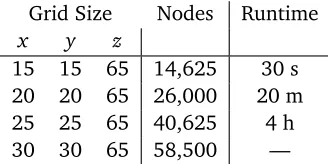
3.4 Analysis of WireX Models . . . 45
3.4.1 Model conversion with decreasing grid size . . . 45
3.4.2 Tradeoff between simulation area and resolution . . . 52
3.5 Summary . . . 53
Chapter 4 Power Blurring HD: A Rapid, Hierarchical Thermal Simulation Technique for 3DICs . . . 54
4.1 Overview . . . 54
4.2 Modeling Assumptions . . . 56
4.3 Chip Characterization for Power Blurring HD . . . 57
4.4 Near/Far Effect: Offset Correction . . . 59
4.5 Extending Power Blurring HD for 3D . . . 66
4.6 Power Blurring HD Algorithm . . . 70
4.7 Discussion . . . 72
4.7.1 Response Mask Model Selection . . . 72
4.7.2 Resolution vs. Transistor Placement . . . 76
4.8 Validation Design (“u60x3”) . . . 78
4.8.1 Response Mask Flipping . . . 89
4.8.2 Approximation of Transistor Channel Sizes . . . 92
4.9 Implementation Details . . . 95
4.9.1 Response Mask Generation . . . 95
4.9.2 MATLABImplementation of Power Blurring HD . . . 98
4.10 Response Mask Variance Study . . . 99
4.11 Memory/CPU Time Model . . . 102
4.12 Summary . . . 106
Chapter 5 Case Study: FFT Processor for Synthetic Aperture Radar . . . 108
5.1 Introduction . . . 108
5.2 Simulation Techniques . . . 110
5.2.1 Overview . . . 110
5.2.2 Background . . . 110
5.2.3 Gradient HeatWave-3DIC . . . 113
5.3 Sample Design and Technology . . . 114
5.4 Model Extraction . . . 116
5.5 Comparison of Simulation Resolutions . . . 119
5.6 Tier-Swapping to Improve the Thermal Profile . . . 125
5.6.1 Technology Changes for Tier-Swapping . . . 125
5.6.2 Comparison of Tier Ordering Choices . . . 127
5.7 Power Density vs Temperature in SAR . . . 131
5.8 Full-Chip Power Blurring HD Simulation . . . 136
Chapter 6 Case Study: Cornell Asynchronous Multiplier/Divider Chip . . . 144
6.1 Chip Design . . . 144
6.2 Test Board . . . 146
6.3 Power Blurring HD Model . . . 151
6.4 Per-Transistor Power Value Extraction . . . 151
6.5 Measurement Setup . . . 153
6.6 Results . . . 154
6.7 Summary . . . 161
Chapter 7 Thermal Measurement of Integrated Circuits . . . 166
7.1 Test Jig for Thermal Measurement . . . 166
7.1.1 Mounting Dice on Heatsinks . . . 174
7.1.2 Heatsink and Circuit Board Assembly . . . 176
7.2 3DM3 Thermal Test Chip . . . 178
7.2.1 Site Types . . . 178
7.2.2 Diode/Resistor Sites . . . 178
7.2.3 Capacitive Filler Cells . . . 180
7.2.4 Ring Oscillators . . . 181
Chapter 8 Conclusions . . . 184
List of Figures
Figure 2.1 Power Blurring Approach . . . 15
Figure 3.1 WireX/PETSc flow . . . 32
Figure 3.2 Six Resistor (6R) Model . . . 34
Figure 3.3 Stackup of MIT Lincoln Laboratory’s 3D Process . . . 35
Figure 3.4 Thermal Layer Diagram for the MITLL 3DM3 process . . . 36
Figure 3.5 Gridding of a Metal Layer in WireX . . . 37
Figure 3.6 Simplified Transistor Layout . . . 38
Figure 3.7 Transistor with Good Grid Alignment . . . 38
Figure 3.8 Transistor with Poor Grid Alignment . . . 39
Figure 3.9 Matrix Structure of WireX Models . . . 43
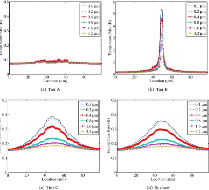
Figure 3.10 Layout for Resolution Convergence Analysis . . . 47
Figure 3.11 WireX simulations for a power source on Tier A . . . 48
Figure 3.12 WireX simulations for a power source on Tier B . . . 49
Figure 3.13 WireX simulations for a power source on Tier C . . . 50
Figure 4.1 Cross-section of a Response Mask . . . 60
Figure 4.2 Simulation Areas for a Response Mask Calculation . . . 61
Figure 4.3 Slices of the response mask for a single transistor . . . 63
Figure 4.4 3D response mask for a 2µm transistor on Tier A . . . 67
Figure 4.5 3D response mask for a 2µm transistor on Tier B . . . 68
Figure 4.6 3D response mask for a 2µm transistor on Tier C . . . 69
Figure 4.7 The Power Blurring HD Algorithm . . . 71
Figure 4.8 Possible locations for square power loads . . . 73
Figure 4.9 Grid Alignment in Standard Cells . . . 77
Figure 4.10 Simplified diagram of an INVX1 standard cell . . . 79
Figure 4.11 Simplified layout of the u60x3 sample design . . . 80
Figure 4.12 Full layout of the u60x3 sample design . . . 81
Figure 4.13 Comparison of simulation results for the u60x3 sample design . . . 84
Figure 4.14 Response Mask Flipping . . . 90
Figure 4.15 Approximation of Transistor Channel Sizes . . . 93
Figure 4.16 Memory usage of WireX and PETSc . . . 105
Figure 4.17 Runtime of WireX and PETSc . . . 105
Figure 5.1 Uniform or coarse grids on a layer . . . 111
Figure 5.2 Thermal-layer stack using mask-layer data . . . 113
Figure 5.3 Stackup of MIT Lincoln Laboratory’s 3D Process . . . 114
Figure 5.4 Stackup of the 3D SAR . . . 115
Figure 5.8 Closeup of the analysis of the 3D SAR with Gradient HeatWave-3DIC . . . 123
Figure 5.9 Histogram of the SAR’s transistor temperatures . . . 124
Figure 5.10 Histogram of the ratio of transistor temperature rise in the SAR . . . 124
Figure 5.11 Stackup of the MITLL process for tier-swapping . . . 126
Figure 5.12 Temperature profiles of the 3D SAR with tier-swapping . . . 130
Figure 5.13 Histogram of SAR channel temperatures with tier-swapping . . . 131
Figure 5.14 Transistor Power Density vs Temperature Rise in the SAR . . . 132
Figure 5.15 Power Blurring HD simulation of the 3D SAR . . . 138
Figure 6.1 Micrograph of the Cornell chip . . . 145
Figure 6.2 Cornell chip unit chain . . . 146
Figure 6.3 Photographs of the test board for the Cornell chip . . . 148
Figure 6.4 Measurement and Power Blurring HD simulation of the Cornell chip . . . 155
Figure 6.5 Measurement and Power Blurring HD simulation of a Cornell chip hotspot . . 156
Figure 6.6 Simulation of the channel temperature in a Cornell chip hotspot . . . 159
Figure 6.7 Power Blurring HD simulation of the Cornell chip . . . 163
Figure 7.1 Custom heatsink . . . 168
Figure 7.2 Custom circuit board, with central cutout . . . 169
Figure 7.3 Custom circuit board for sign of life testing . . . 172
Figure 7.4 Perf board for sign of life testing . . . 173
Figure 7.5 Full-spec board under test . . . 174
Figure 7.6 EFD Ultra 870 epoxy depositor . . . 175
Figure 7.7 Full-spec board with chip mounted on a heatsink . . . 177
List of Tables
Table 1.1 Thermal conductivity of low-k materials . . . 4
Table 2.1 Correspondence between Thermal and Electrical Units . . . 14
Table 3.1 Approximate Six-Resistor Macromodel Runtimes in fREEDA . . . 30
Table 4.1 Runtimes for the u60x3 sample design . . . 83
Table 4.2 Per-transistor temperatures for the u60x3 sample design . . . 87
Table 4.3 Channel temperature rises for the u60x3 sample design . . . 87
Table 4.4 Per-transistor temperatures for the u60x3 sample design with flipping . . . 92
Table 4.5 Per-transistor temperatures for the u60x3 sample design with 4µm responses 94 Table 4.6 Per-transistor temperatures for the u60x3 sample design with 2µm responses 95 Table 4.7 Power Blurring HD Variance Study: Channel Temperature . . . 101
Table 4.8 Power Blurring HD Variance Study: Maximum Temperature . . . 101
Table 4.9 Comparison of WireX and Power Blurring HD for the u60x3 sample design . . 106
Table 4.10 Comparison of RMSE for various response mask choices for the u60x3 sample design. . . 107
Table 5.1 Comparison of SAR Simulation Results . . . 119
Table 5.2 Comparison of temperature rises with tier-swapping . . . 128
Table 5.3 Comparison of memory and runtime requirements for thermal analysis of the SAR . . . 142
Table 6.1 Comparison of memory and runtime requirements for thermal analysis of the Cornell chip . . . 154
Table 6.2 Simulated mean and maximum temperatures of a Cornell chip hotspot . . . 161
Table 7.1 Estimated Capacitive Filler Cell Values . . . 181
Table 7.2 3DM3 Site Descriptions . . . 182
Chapter 1
Introduction
The move to silicon-on-insulator (SOI) processes, porous low-k dielectrics and vertical stacking,
as seen in three dimensional integrated circuits (3DICs), have made it increasingly challenging to
both predict and control device temperatures. Newer technology nodes have also brought about
increased power densities which further exacerbate the problem. We can no longer just add a bigger
heatsink and hope that our thermal problems will go away.
The 2009 International Technology Roadmap for Semiconductors (ITRS) notes that “the required
electrical, thermal, and mechanical simulations must be performed with consideration of the die
and the system, and[that]this is possible only with communication enabled by co-design tools”[1].
New simulation tools that are capable of turning linear design flows into multi-physics, iterative
design flows are necessary to enable this type of co-design.
1.1
Motivating Factors
We begin by exploring the need for a transistor-level thermal analysis tool that is both fast and
accurate. This will be done by walking through a diverse set of motivating factors. These factors
have been broken into the following areas:
• Device Effects
• Porous Low-k Dielectrics
• Vertically Stacked Circuits (3DICs)
• Reliability Concerns
• Modeling Granularity Requirements
• Interconnect Effects
While this list may appear incongruous at first, we will see that all of these areas play a role in
supporting the need for both speed and accuracy in thermal modeling. In fact, it is because of the
broad range of competing effects that thermal management has become increasingly challenging.
1.1.1
Timing Closure
The critical path in a circuit is the path that limits the frequency of the overall circuit. Critical
paths are typically identified by register transfer level (RTL) synthesis software (such as Synopsys
Design Compiler). The sensitivity of the propagation delay of the circuit varies with temperature,
supply voltage, and input slew rate. Cheng et al. presented simulation results that show that the
on-chip temperature variation must be considered in timing verification[2]. It is important to note
that rising temperature does not always have the same effect on the propagation delay of all nets.
Lasbouygues et al. investigated a phenomenon known as “timing reversal”, where the order of nets
from fastest to slowest can change, based on temperature[3].
This presents a major issue for circuit designers, who rely on synthesis tools’ determination of
the critical net to pick clock frequencies for the system. Currently, Synopsys evaluates all of the
design cells at the same temperature. This means that the delay reversal phenomenon would not be
apparent until after a transistor-level thermal analysis was done.
Since the designer does not have a way to easily iterate between Synopsys and a thermal analysis
will not be able to be designed to meet the true performance cap for the technology.
To overcome problems such as this, thermal simulation must be included early on in the design
process, in a manner that allows the designer to make informed decisions. Since synthesis is a
relatively fast process (usually less than an hour), any tools that will run iteratively with these tools
must also be able to run in a similar time frame.
1.1.2
Device Effects
The ITRS roadmap predicts that power density will continue to increase for both cost-performance
and high-performance microprocessors[1]. As power density increases, it becomes more challenging
to remove heat from the device. This is because the heat must cross the thermal boundaries between
the source (typically inside the channel of transistors) and the heatsink. Every material has an
intrinsic thermal resistivity which can be expressed in meters Kelvin per watt. In a 1D sense, doubling
the power that must cross the same area of epoxy will double the temperature difference across the
epoxy. In a 2D system, this can be compensated for by increasing the footprint of the chip, which
gives more parallel paths for heat to exit through the epoxy. This can by prohibitively expensive, as
it requires the chip area to be increased. It has been found that packaging cost increases by $1 per
watt when the total power dissipation is greater than 35-40 watts[4].
IOFFhas been found to increase at approximately 5 times per generation[5,6]. IOFFalso increases
exponentially with temperature[4, 5]. Rastogi et al. investigated leakage power in 65 nm devices,
and found that 20% of the total switching current was leakage current[7]. Subthreshold leakage,
given by
Isub=I0exp
V
GS−VTH−VOFF
nVT 1−exp
−VDS
VT
(1.1)
I0=µ0Cox Weff/Leff
VT = kT
q (1.3)
where VOFFis the offset voltage in the sub-threshold region, was found to be the major contributor
to total leakage.
Drain current is more difficult to predict, as it is affected by both the threshold voltage and
carrier mobility. VTH, the threshold voltage, and carrier mobility both decrease as temperature
increases. Drain current, however, increases with declining threshold voltages, and decreases as
carrier mobility drops. Park et al. studied 0.6µm devices and found that whenVDDVTH, carrier
mobility accounts for most of the change in drain current. WhenVDDapproachesVTH, the change in
VTH begins to take over as the primary effect[8].
1.1.3
Porous Low-k Dielectrics
Recent technology nodes have begun moving to porous low-k dielectrics in an effort to overcome
signal integrity issues. These dielectrics are designed to decrease parasitic capacitance between
wires, but also have a significant impact on the thermal performance of the circuit.
Porous dielectrics are made by removing atoms from otherwise non-porous materials. This
decreases the thermal conductivity of the dielectric, and presents a thermal barrier. Due the
sponge-like nature of these dielectrics, glue layers are often used to seal the dielectrics. While little data is
available on the exact glues that are used, it is reasonable to assume that they will have a fairly low
thermal conductivity.
Table 1.1: Thermal conductivity of low-k materials. (After[9])
Material Thermal Conductivity (W·m−1·K−1)
Aerogel 0.14±0.02
LKD-5109 0.19±0.03
Orion 2.2 0.16±0.02
Philk 0.15±0.03
Porous SiLK 0.11±0.02
In the 180 nm technology node, SiO2(glass) was used as an interlayer dielectric (ILD). SiO2has
a thermal conductivity of approximately 1.1 W·m−1·K−1 at 300 K. Table 1.1 shows the thermal
conductivities for common porous dielectrics[9]. The move from 180 nm to 45 nm has seen a shift
of an order of magnitude in the conductivity of common dielectrics.
The disparity between interconnect and the dielectric is not likely to decrease. Carbon nanotubes
are currently being investigated as a possible replacement for traditional interconnects. These
structures are highly conductive along their axis, and have been found to have conductivities up to
6600 W·m−1·K−1 [10].
1.1.4
Vertically Stacked Circuits (3DICs)
The introduction of three dimensional integrated circuits (3DICs) has created a new obstacle for
thermal engineers. In 3DICs, multiple wafers are stacked vertically. Many techniques are currently
being researched for vertical integration[11, 12].
When individual wafers are fabricated with SOI processes, the bulk silicon “handle” can be
entirely removed from upper tiers. Akturk et al. have shown that “heat flow is blocked strongly
by the oxide layers between the stacked chips”[13]. This is a significant divergence from 2D bulk
processes, where power sources were assumed to be on top of a large silicon substrate. The thermal
conductivity of silicon is nearly 100 times larger than that of standard dielectrics, and 1000 times
that of porous dielectrics.
New design-for-thermal approaches will be required in these technologies to appropriately
dissipate heat. Such approaches will need to take advantage of the disparity between interconnect
and dielectric thermal conductivities. From a design perspective, it is not yet clear what the optimal
arrangement of active devices is. For instance, if the memory is the most temperature-sensitive
part of the design, it may make sense to place the memory closest to the heatsink. However, in
interconnect-heavy designs that have numerous blocks which connect to the memory, it may be more
beneficial to place the memory in the middle. In this case, the processing elements could be placed
that reach the memory to serve as heat dissipation paths.
1.1.5
Reliability Concerns
Thermal effects have a profound impact on the reliability of integrated circuits. Electromigration
induced mean time to failure (MTTF) decreases exponentially with temperature. As average
temperatures rise, this can become a significant mechanism for circuit failure.
It has been found that temperature can vary by tens of degrees from the center to the edge of a
chip[2]. Thermal analysis tools must be able to simulate the circuit at a fine enough granularity to
capture these effects.
1.1.6
Modeling Granularity
The current trend in thermal modeling is to obtain power dissipation numbers at the module level.
These average power dissipation numbers are then spread evenly across the entire module. Park et
al. have compared simulations with 5µm×5µm and 100µm×100µm resolutions. It was found
that very fine meshing performs much more accurately in terms of showing micro-scale hot-spots. It
was also found that there is a discrepancy in the average chip temperature obtained with the coarse
and fine simulations[14].
In digital circuits, clock buffers typically account for 40-70% of the total power dissipation.
High-power clock buffers are often interspersed with lower High-power logic. While the average temperature
far from these clock buffers may not be significantly impacted, it can have a significant impact on
individual transistors that are very close to the buffers. Liu et al. found that wires under these buffers
(buried interconnect) can have a large impact on device temperature[15].
1.1.7
Interconnect
Interconnect structures are highly dependent on temperature both in terms of reliability as well
temperature level when the temperature is increased by 7.8 °C above 25 °C. It is further shrunk by
90% when the temperature increases from 27.5 °C to 52.5 °C[16].
Chen et al. found that as interconnect temperatures rose from 25 °C to 100 °C (a typical operating
range,) the delay went up by 30%[17]. It was also found that for parallel aluminum lines in a
dielectric of SiO2 the temperature is reduced due to thermal coupling by as much as 35% relative to
the case of an isolated line. This highlights the need to include wiring in the thermal model.
Chiang et al. examined Joule heating in interconnects at the 100 nm node and found that even in
low-k dielectrics, using a sufficient number of vias can overcome the thermal effects of moving away
from SiO2. This was also found to hold when the dielectric was air.[18]. While this is not directly
applicable to the full-chip case, it highlights the effect of planned structures for heat removal.
1.1.8
Summary
While the motivating factors themselves are diverse, they all serve to point out the necessity of
accurate thermal analysis. By accurately anticipating thermal phenomena we will be able to able to
identify “slack” between thermal design goals and other design criteria. Available slack can then be
reallocated to mitigate other design challenges.
1.2
Original Contributions
This dissertation advances the state of the art of thermal analysis in order to allow the thermal
performance of complex circuits to be understood more fully. This is intended to help make
truly multi-physics design flows feasible in the future. The major contributions presented in this
dissertation are:
1. A method for dividing the thermal response caused by a heat load into a high fidelity “near
response” and a lower fidelity “far response.” This method is used in Chapter 4 to implement
a high definition version of the Power Blurring approach (“Power Blurring HD”) to enable
while operating at a runtime that is similar to common digital design tools. This approach is
estimated to yield three orders of magnitude of improvement in the memory use and up to six
orders of magnitude of improvement in runtime over WireX for a 3 mm×3 mm 3-tier circuit
modeled with a 0.1µm×0.1µm grid.
2. A custom thermal network extractor (“WireX”) suitable for calculating “near responses” is
presented in Chapter 3 to extract resistive mesh-based thermal models that include the full
structure of three dimensional integrated circuits to appropriately model heat flow in SOI
3DICs. Sparse matrices are used to allow the extractor to handle thermal networks that contain
tens of millions of nodes.
3. A method for preparing circuits for thermal measurement using custom heatsinks and printed
circuit boards is presented in Chapter 7. The presented approach is designed to come as close
as possible to placing the chip on an ideal heatsink to allow measured results to be directly
comparable with simulations that use simple boundary conditions, namely adiabatic top and
side boundary conditions along with a fixed boundary condition on the bottom.
1.3
Organization
The remainder of this dissertation is organized as follows. In Chapter 2 background information
is presented along with an overview of related work. In Chapter 3 the WireX resistive mesh-based
thermal network extractor is introduced to accurately model the full structure of small areas of
three dimensional integrated circuits. In Chapter 4 a high definition Power Blurring-based approach
named “Power Blurring HD” is presented to enable chip-scale thermal analysis with junction-level
accuracy while operating at a runtime that is similar to common digital design tools. In Chapter 5 a
case study of a 3D FFT processor for synthetic aperture radar (SAR) is presented. In Chapter 6 a case
study of a 3D asynchronous circuit is presented which includes a comparison of the temperature
profile from a chip-level Power Blurring HD simulation with measurement. In Chapter 7 a method
introduced. Finally, Chapter 8 wraps up the work presented in this dissertation and provides tips for
Chapter 2
Background
For modern very large scale integration (VLSI) circuits, the exact calculation of the thermal profile is
a daunting task. High-performance integrated circuits (ICs) routinely contain millions of logic gates,
memory cells and other structures. Each of these structures has its own complex three-dimensional
structure, including wires, vias and transistors. The thermal properties of the materials used to
fabricate these circuits varies highly. In deep sub-micron technology nodes, interconnects typically
have thermal conductivities several thousands of times higher than the surrounding dielectric
material.
As the thermal conductivity of the components of the IC stackup diverge, the effect of detailed
structures on the overall thermal profile becomes more pronounced. New integration technologies
such as three-dimensional integrated circuits (3DICs) create additional complications as devices are
moved further away from the heatsink.
In this chapter, we will begin by overviewing the fundamentals of heat transfer as it pertains to
IC thermal analysis. We will then turn our attention to the state of the art of IC thermal analysis and
2.1
Thermal Simulation
The temperature profile in an integrated circuit (IC) is generally determined in one of two ways.
The first method involves discretizing the heat diffusion equation. This approach is used by the finite
element method (FEM) and the finite difference method (FDM). The second method for determining
the temperature profile is to use the boundary element method (BEM) which typically relies on
Green’s function.
2.1.1
Background
The heat diffusion in a solid object is governed by the following differential equation[19]:
ρcp∂T(x,y,z,t)
∂t =∇ ·[κ(x,y,z,t)∇T(x,y,z,t) +g(x,y,z,t) (2.1)
subject to the general boundary condition
κ(x,y,z,T)∂T(x,y,z,t)
∂ni +hiT(x,y,z,t) = fi(x,y,z) (2.2)
where T is the temperature (K), g is the power density of the heat sources (W·m−3), κis the
thermal conductivity (W·m−1·K−1),ρis the density of the material (kg·m−3),cpis the specific heat (J·kg−1·K−1),hi is the heat transfer coefficient at the boundary surfacei(W·m−2·K−1), fi(x,y,z)
is an arbitrary function at the surfacei, andni is the outward direction normal to surfacei. Methods for efficiently solving this problem for integrated circuits rely on simplifying either the
model of the circuit, the driving function to the circuit or both. Examples of simplifying the circuit
model include the finite element method were the model is discretized into blocks of material with
single thermal conductivities and the boundary element method where layers are homogenized to
have a single thermal conductivity per layer.
Examples of simplifying the driving function include representing the power dissipated in
individual transistors as a large area heat load and applying average power values to transistors
Simplifications are used to speed up the amount of time it takes to solve the problem, but are
also used more generally to decrease the complexity of the problem so that it is tractable on a given
set of hardware resources. Without simplifications, nonlinearities in the heat diffusion equation
require that the interaction between the electrical, mechanical and thermal domains be modeled.
The degree to which these interactions can be considered will depend greatly on the extent to which
the models for each of these domains are simplified.
2.1.2
Finite Element
/
Finite Difference Method
Both the finite element method (FEM) and the finite difference method (FDM) enjoy widespread
use for many types of physical problems. These approaches are suitable for physical problems whose
underlying physics can be described with partial differential equations (PDEs). Both methods solve
the PDEs by dividing the material into smaller volumes. This allows for the solution of problems
that would otherwise be intractable. The trade-off over an analytical solution to the PDEs is in the
accuracy of the solution.
The primary difference is that FDM approximates the differential equation, while FEM
approxi-mates its solution. FDM is generally restricted to rectangular shapes, while FEM is able to handle
complex geometries and boundary conditions. The major disadvantage of both methods is that their
accuracy is highly dependent on the mesh density. For any given problem, an application-specific
mesher will allow for the highest performance possible using these methods. This has the downside
of limiting the type of geometries that the solver can handle.
FEM/FDM solvers are typically able to solve systems that include between one and twenty
million elements. The upper range of this scale is generally reserved for highly regular geometries.
For a 1 cm×1 cm IC, a 10µm×10µm grid would require one million elements per vertical layer.
For even a modest number of layers, this quickly approaches the upper limit of FEM/FDM solvers.
The number of points for which temperatures are returned also depends highly on the solver.
Some FEM/FDM solvers only return one temperature per element. Others, such as Creo
across an individual element.
Implementations
Cheng et al. developed ILLIADS-T to predict temperature-dependent reliability problems in VLSI
circuits[2, 20]. ILLIADS-T can be used to guide module placement, packaging as well as timing
verification. A mixed 1-D/3-D approach is adopted, and the heat equation is solved with a numerical
FD approach. An RC network is created that is analogous to the FD heat conduction problem.
This is then solved by either a sparse matrix routine or a successive over-relaxation routine. The
chip substrate is modeled in 3D, while 1D thermal resistances are used for package and heatsink.
Capacitors are removed for steady state, and nodal analysis of the final resistive network is performed.
The resulting admittance matrix is then solved for temperature.
The electrical and thermal problems are decoupled, allowing for a significant speedup over
combined electro-thermal modeling. A power calculation is first done at room temperature. The
temperature values from an initial thermal simulation based on those power values are then fed back
into the power simulator. The authors note that this usually only takes a few iterations to converge.
The authors found that it is impractical to allocate one or more grids to each gate. Griding
is fixed in thez−direction, but is dynamically chosen in the x−and y−directions based on the
temperature gradient. Transistor active areas are extracted from the layout. A tester chip with ring
oscillators and diodes is used to test the method, and good agreement is found.
2.1.3
Boundary Element Method
The second method for determining the temperature profile is to use the boundary element method
(BEM) which typically relies on Green’s function. Green’s function is used to describe the temperature
response to a unit power source. Chip-level solvers combine these responses to calculate the full
response. While an individual calculation of Green’s function is inexpensive, these solvers require
up toNsource calculations, where Nsource is the number of independent heat sources in the circuit.
Table 2.1: Correspondence between Thermal and Electrical Units
Thermal Units ⇔ Electrical Units Temperature (K) ⇔ Voltage (V)
Power (W) ⇔ Current (A)
Thermal Resistance (K·W−1) ⇔ Electrical Resistance (V·A−1) Thermal Capacitance (W·s·K−1) ⇔ Electrical Capacitance (A·s·V−1)
homogeneous, which severely limits the applicability of such approaches to 3DICs.
In[21]Cheng and Kang develop a fast thermal analysis (FTA) approach that is integrated into
the ILLIADS-T framework. FTA is used to efficiently pinpoint hot areas for reliability analysis and is
based on the fact that the dimension of gate-level heat sources are small compared to the chip size, so
they are viewed as being located in a relatively infinite body. Concise analytical formulae are derived
for hot-spot identification at the cost of model flexibility – materials are infinitely large horizontally.
Solder, packaging and ambient are modeled as a single effective heat transfer coefficient. The
assumption is made that the dimensions of gate-level heat sources are small as compared to the chip
size. This allows the power sources to be viewed as being location on a relatively infinite body.
In [22] Zhan and Sapatnekar convolved the power distribution with the underlying Green
function to obtain the temperature field. Frequency domain computations with the discrete cosine
transform (DCT) result in a significant improvement in efficiency. Runtime isO(Ng c×log(Ng c)). An
M×N grid is used for their power sources, and power is distributed evenly over those areas.
2.1.4
Lumped Element Method
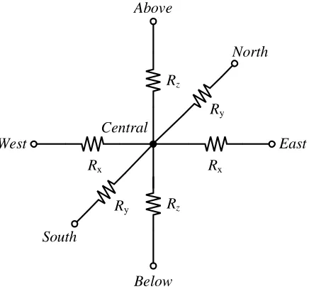
The Lumped Element Method (LEM) allows the use of off-the-shelf circuit solvers to solve complex
thermal problems. This approach is particular appealing for the thermal modeling of integrated
circuits, since it allows the use of tools that are already available for the electrical simulation of the
IC.
Since electrical and thermal problems are solved with identical differential equations, we are
able to perform a substitution of variables to turn a thermal problem into an electrical one. The
*
=
Impulse Response
Power Map
Full-chip Response
Figure 2.1: The Power Blurring approach[4]calculates a full-chip thermal response by convolving thermal impulse responses with a power map.
Due to the temperature dependence of some electrical parameters (such asVTH, the threshold
voltage of a transistor), it is often necessary to simultaneously examine both the thermal and the
electrical problem.
The electro-thermal approach allows for the simultaneous solution of both the electrical and
thermal problem.
2.1.5
Power Blurring
Power Blurring is a superposition-based approach that uses techniques similar to those used for
image blurring filters. In a Gaussian blur, each pixel in the input image is convolved with a Gaussian
distribution to produce the blurred version. A similar effect is seen in photography where point
sources in out-of-focus portions of the picture are convolved with a circular distribution to produce
“bokeh”. In Power Blurring, thermal impulse responses are convolved with the power map to
calculate the full-chip thermal profile (see Figure 2.1).
This approach shares many similarities with Green’s Function-based approaches, however its
major advantage is that it does not require an analytical solution to the heat equation for the
geometry of interest. The need for an analytical solution limits Green’s Function-based solvers to
handling only simple geometries. In the literature, this usually takes the form of calculating the
thermal response to an impulse heat source located in the middle of an infinitely large plane of
silicon. While multiple homogeneous layers of material can be stacked with such approaches, the
complex metallization structures found in integrated circuits.
The Power Blurring approach was initially presented in[4]. A 1 cm×1 cm chip was analyzed
using impulse responses generated with ANSYS. The ANSYS model placed heat loads on the entire
1 cm×1 cm silicon substrate and used a model resolution of 250µm× 250µm. No detail was
included other than the heat load and the substrate. A speedup of three orders of magnitude was
found over a full model for the circuit in ANSYS.
The Power Blurring approach was then extended in[23]to consider the effect of pyramid-shaped
models that included packages and to use the Method of Images to compensate for the edge effect of
the chip on the thermal response.[24]showed how impulse responses could be parameterized.[25]
extended the approach to consider transient thermal simulations.[14]examined the effects of using
finer models, down to 5µm×5µm to consider transistor-level simulations. Heat sources were
modeled on simple substrates without the consideration of interconnect. The use of the Fast Fourier
Transform (FFT) and matrix multiplication were used to solve the problem in the frequency domain,
bypassing the need for the convolution step.[26]showed how the Power Blurring approach could
be extended to consider 3DICs. The 3D stack considered silicon and bonding layers at the chip-scale,
but did not consider the effect of the interconnect structures.[27]showed experimental results
comparing the Power Blurring approach to measurement for a 2DIC.[28]implemented an Adaptive
Power Blurring approach that was able to consider the non-linearity of the silicon substrate’s thermal
conductivity with temperature.
Discussion
Power Blurring uses pixel-based impulse responses for the convolution. This allows for the use
of a variety of tools to generate the impulse responses. Finite element method (FEM) and finite
difference method (FDM) solvers are well suited to handling problems with arbitrary geometries.
Using these tools allows the consideration of impulse responses for complex models, such as that of
an integrated circuit with full-fidelity layout information. This becomes particularly important in
complex wiring and finally to a heat sink at the bottom of the stack. The metallization can no longer
be ignored in such a structure. Furthermore, since transistors in silicon-on-insulator designs are
no longer sitting directly on a large silicon substrate, the exact geometry of the silicon-on-insulator
islands must also be considered. This increases the modeling burden as the model fidelity must be
sufficiently high such that these effects can be captured.
Generating the impulse response for such a circuit is not trivial. Even though commercial finite
element solvers are capable of handling arbitrary geometries, the aspect ratio of the layers in a
typical integrated circuit can present a problem. Tools often need specialized algorithms to mesh
such a structure. Even with these algorithms, the number of elements required to accurately capture
the material information can be far greater than the tools are capable of handling. Additional
complications arise when attempting to convert the chip layout into a physical model. The majority
of the finite element solvers do not provide built-in methods for generating models from layout data.
Even if these complex geometries could be drawn by hand, the burden of model creation would be
overwhelming. To be of use to a designer, the tool must be able to directly use the layout database.
2.2
Thermal Macromodeling
In this section we will look at methods of performing thermal macromodeling. While macromodeling
is often avoided while examining small areas, it comes critical for full-chip simulation where
performing a full-fidelity simulation would be computationally intractable. Macromodeling allows
for problem-order reduction, typically at the expense of accuracy. We will later look at hierarchical
techniques which use a divide-and-conquer approach, which greatly reduces the problem size while
having a smaller impact on accuracy.
General FEM and FDM solvers are suited to handling arbitrarily complex geometry, however this
comes at the cost of computation time and numerical stability. In many cases, meshing errors are
2.2.1
Block Effective Thermal Conductivity
When the problem is defined in terms of blocks of material, an effective thermal conductivity can be
used for the region. Traditionally, heterogeneous blocks are split into unit cells which enable the
development of an analytical model for the material[30].[31]presents a method of using an FEM
solver to determine the effective conductivity, however it is computationally intensive and limited to
material that are statistically homogeneous.[32]presents a technique to combine various statistical
conductivity models into a combined model. These approaches become ill-suited when the material
is no longer statistically homogeneous. This is becoming increasingly evident in ICs as the disparity
between the thermal conductivity of the inter-layer dielectric (ILDs) and the metal wires continues
to increase. This creates materials with effective thermal conductivities that are strongly dependent
on the design artwork.
Due to computational limits, several works have considered simple approximations for the
thermal conductivity of portions of an IC. In [29] and [33] the weighted average of thermal
conductivities of the materials present in each block are used. This model is often selected due to the
lack of placement and routing data at the time of thermal analysis. In[34], only the crossectional
area of metal structures at the edges of the block are used to construct the weighted average. This
technique allows for the extraction of different conductivities in the+x,−x,+y,−y,+zand−z
directions. This approach is suitable when the majority of wires cross the block boundary and also
connect to circuit elements near the center of the block.
While the statistical models are not generally applicable to integrated circuits, it should be noted
that the parallel model and the series models respectively represent theoretical lower and upper
bounds on thermal conductivity. The conductivity computed based on the weighted average tends to
fall in the middle of these bounds for non-extreme cases.
2.2.2
1-D Effective Thermal Conductivity
Initial approaches to estimating circuit operating temperature were based on the calculation of
ΘJC, the junction to case resistance, andΘCA, the case to ambient resistance. These 1-D thermal
resistances have typically been used to aid in the selection of packages and heatsinks, as well as for
airflow calculations.
While 1-D thermal parameters no longer provide an acceptable level of temperature estimation
for on-chip structures, they are still widely used to model the effective thermal resistance of mounting
epoxy and heatsinks. In[36]it was found that the time constants associated with a block on the chip
are on the order of 10−4s, which is much smaller than the time constant for the heatsink. Because
of this, the dynamic effects of the heatsink can be ignored. This allows us to model the heatsink as a
1-D conductivity without compromising the accuracy of on-chip areas.
2.3
Circuit Simulation
This section presents an overview of circuit simulation topics relevant to the simulation of thermal
networks, such as those used in the Lumped Element Method.
2.3.1
Modified Nodal Admittance Matrices
Modified Nodal Admittance Matrices (MNAMs) provide a method for describing a circuit in matrix
form. The MNAM for a network is formed by applying Kirchoff’s Current Law (KCL) to each node of
the network. By describing a circuit in this manner, the DC solution to the circuit can be computed
with a single matrix solve.
The system of equations formed by applying Kirchoff’s Current Law (KCL) to each node of the
network is represented in matrix form as[37]:
which can be written in an expanded form as: Y E F D v i = J K (2.4)
whereYis the circuit’s nodal admittance matrix,vis the vector of terminal node voltages, andJand
Kare the source vectors, andE,FandDare a type of incidence matrices that allow circuit elements to be included that require more than a simple admittance description.
One of the advantages of using this type of approach, is that the effect of any one circuit element
in the design can be represented as a stamp matrix. The use of stamps allows the matrix contribution
of an element to be identified ahead of time and then easily superimposed on the total matrix. This
makes the creation of the matrix for the full circuit very systematic, allowing it to be generated easily
by a computer.
Of interest to this work are two stamps: one for an admittance and one for a voltage source. The
use of these two stamps will enable the creation of a resistive mesh to describe the thermal network
of a circuit.
For an admittance from nodeito j, the stamp is:
vi vj
ii y −y
ij −y y
(2.5)
in theYportion of the main matrix.
source stamp is:
vi vj i
ii 1
ij −1
1 −1
(2.6)
in the main matrix, and
ii ij E (2.7)
in the source vector.
A full description of the use of MNAMs for general circuits and additional stamps can be found
in[37].
2.3.2
Sparse Matrix Techniques
A sparse matrix is defined as any matrix for which sparse matrix techniques are more efficient
than non-sparse matrix techniques. This is generally the case when the majority of entries in the
matrix are zero. In the case of a resistive mesh MNAM, each row in the matrix will have up to
seven non-zero entries: one for the node corresponding to that row and one for each node that it is
resistively coupled to (typically six for nodes in the center of the mesh.) For a square matrix with
25,000,000 rows and 25,000,000 columns, this yields a matrix with less than 0.000035% of entries
being non-zero. Attempting to store such a matrix in memory without the use of sparse matrix
techniques would require 1455 TB of memory, assuming the use of 32-bit floating point numbers for
all entries. This is well beyond the scope of the storage available on modern desktop machines.
Sparse matrix techniques allow for the efficient storage of such matrices. Sparse matrix
of rows and columns, only non-zero entries are stored. The downside to these approaches is that the
access time for individual elements is no longer O(1), but instead depends on the data structure
used to store the matrix contents.
2.3.3
Resistive Mesh Compaction
When the Lumped Element Method (LEM) is used, the results can be expressed in terms of a network
(circuit) of resistive elements. When the netlist for such a network in read into a circuit simulator
(such as SPICE or fREEDA) it is converted into an admittance matrix. Gaussian Elimination can then
be used to reduce the order of a network’s admittance matrix. Gaussian Elimination is suitable for
problems where the total number of elements is large compared to the number of heat-generating
elements.
The effect of Gaussian Elimination is to remove a row and column from the admittance matrix
for every internal node in the circuit that does not have an external current source applied to in. In
terms of the circuits generated by applying LEM, this means we can remove every node from the
matrix that does not generate power (i.e. have a current source connected to its central node.) The
downside to this compaction is that we lose the ability to measure temperature at the eliminated
node.
For ICs, the extent of the reduction is highly dependent on how the circuit is modeled. If the
circuit is gridded into volumes that are larger than the individual elements, very few elements will
be eliminated. If the volume size is very small compared to the circuit elements, then the savings
will be substantial. At a minimum, the condensed admittance matrix must contain: (a) edges of
the volume that connect to other volumes or have boundary conditions applied to them, (b) nodes
that generate power (i.e. are connected to external current sources) and (c) other nodes of interest
where the temperature values are desired.
We will now briefly introduce the nodal admittance matrix (NAM) which is used by SPICE and
fREEDA to represent the network. Presently, a modified nodal admittance matrix (MNAM) is used in
expressed as an external current source.
The MNAM for a network is formed by applying Kirchoff’s Current Law (KCL) to each node of
the network. This system of equations can be represented in matrix form as:
Yv=J (2.8)
whereYis the matrix’s admittance matrix,vis the vector of terminal node voltages, andJis the vector of external current sources. Expanding the matrix equation yields:
y11 y12 . . . y1M
y12 y22 . . . y2M
..
. ... ... ...
yM1 yM2 . . . yM M
v1 v2 .. . vM = J1 J2 .. . JM (2.9)
Yis then re-expressed as:
Y= A B C D (2.10)
whereArepresents the portion of the matrix that includes rows and columns for the nodes which will not be removed. The full equation then becomes:
A B C D v1 .. . vN
vN+1
.. . vM = J1 .. . JN 0 .. . 0 (2.11)
reduced form:
A−BD−1C
v1 .. . vN = J1 .. . JN (2.12)
IfDis symmetric and positive definite, Cholesky factorization can be used to computeD−1[38]. The condensed admittance matrix is then solved to obtain temperatures at each node. This is often
done with LU decomposition[39].
2.4
Thermally-Aware Design
The vertical arrangement of three-dimensional ICs (3DICs) is widely viewed as having the potential
to exacerbate thermal issues. This structure is likely to cause the on-chip temperature profile to be
much more heavily dependent on device placement and interconnect patterns.
The anticipated thermal issues associated with 3DICs have spawned interest in thermally-aware
design techniques. These are typically either focused on the floorplanning stage when logical blocks
are placed, or at the place-and-route (P&R) stage where individual gates are placed and interconnect
is added. Design techniques are primarily concerned with adding and placing through-silicon vias
(i.e. vias that connect between tiers in a 3DIC) or with altering the placement of cells.
2.4.1
Thermally-Aware Place and Route
Modern place and route tools are capable of balancing a large number of conflicting design
parame-ters such as wirelength, signal integrity and antenna effects. Each of these parameparame-ters can be thought
of as a spring pulling certain circuit elements towards each other. The spring constant of each spring
would be related to the cost of the individual decisions. For instance, two connected circuit elements
that are very sensitive to wirelength would have a spring with a large spring constant binding them
lowest-cost design.
One way of performing thermally-away place and route is to add an extra force the pulls circuit
elements towards the heatsink. This must be carefully balanced with other parameters so that
high-power blocks can be moved closer to the heatsink, without disturbing the routability of the
design.
2.4.2
Thermal Via Placement
In addition to the analysis of the thermal performance of 3D circuits, this dissertation also examines
methods for mitigating thermal gradients. The majority of the prior work in this area has been
focused on the placement of thermal vias, which will be discussed here.
It has been found that even after thermally-driven floorplanning, and place and route, on-chip
temperatures can still be too high[40]. Thermal vias offer an additional method of coping with
the thermal landscape of 3DICs. Thermal vias need not be electrically connected to other circuit
elements, however there are many cases when doing so will allow the vias to serve multiple purposes
(e.g. signal integrity, power delivery and thermal problem mitigation.) The efficacy of such vias is
highly dependent on their placement and structure.
When placed manually, thermal vias are typically placed in regions of high power density.
The ultimate goal is to minimize both the maximum on chip temperature, as well as stabilize
the temperature gradient. This must be done with careful consideration of the impact on design
routability. Thermal vias tend to be many times larger than traditional interconnect vias, and in
many cases create routing blockages on all layers of the tiers that they pass through.
The actual structure of thermal vias is dependent on the process that is being used. In the
MIT Lincoln Laboratory 0.18µm FDSOI 3D process, inter-tier signal vias are often used as thermal
vias. In this process, a typical interconnect via is 0.3µm2 while a through-silicon via (TSV) is 1.75
µm2. TSVs are particularly suitable for being used as thermal vias since they cut through all layers,
including oxide and bonding layers between tiers. This gives them a direct path to the top-level
effective conductivities of individual tiers in the MIT process. Other schemes for through-silicon vias
cut through the entire wafer, including the bottom tier’s bulk or handle. In these cases, thermal vias
have direct access to the heatsink.
Several works have studied algorithms for thermal via placement at various stages of the chip
design cycle. The insertion of “dummy thermal vias” was first introduced by Chiang et al.[41].
Cong and Zhang looked at via placement during routing using path counting and heat propagation
to pick the shortest path[40]. Goplen and Sapatnekar grouped intertier vias into separate regions
with uniform via densities[42]. Their algorithm reduced the via count by 48.5% and was able to
lower the maximum temperature by 47.3%. They found that just placing thermal vias in hot spots
has little impact on reducing thermal problems. The algorithm proposed by Li et al. was able to
reduce the number of thermal vias by 15%[43]. Wong and Lim considered thermal via placement
during floorplanning using a random-walk based thermal analysis. With a thermal via density of
<3%, they were able to drop the maximum temperature by 17%, while only increasing area by 4%
and wirelength by 1%[44]. Hua found that interconnect-heavy designs such as an FFT can become
unroutable when thermal via cell density exceeds 20% (equivalent to 5% thermal via density)[11].
The coincides well with what Rahman and Reif estimated to be a realistic inter-tier via density (4%
of area) and would give a 2-3x reduction in the effective thermal resistance of the ILD[45].
2.5
Summary
There is a significant gap between the thermal analysis approaches found in material science and
electrical engineering. In material science, the exact construction of the object is not well known,
however the materials are homogeneous and can be broken into “unit cells” which are repeated to
form the material. Statistical models are well developed and highly applicable to many of these
problems.
Thermal analysis in electrical engineering has a different set of problems: the exact material
composition and arrangement is well known, however the objects are prohibitively complex. This
based on the exact structure.
The problem is exacerbated by the move to new technology nodes, where the assumptions used
for thermally modeling prior nodes are no longer appropriate. Two examples of this are the move
from bulk to SOI processes, and the move to porous low-k dielectrics. The move to SOI imposes a
significant restriction of the choice of thermal simulation technique. Many techniques have been
specially formulated with the assumption that the active devices are located on top of a nearly
infinitely large block of silicon. The move to SOI significantly blocks the ability for heat to move
down to the heatsink, and the move to porous dielectrics affects the ability for heat to move laterally
in the interconnect regions.
The assumption that the path through the silicon handle will dominate heat conduction has
resulted in models that do not consider the effect of interconnect. Moving to 3DICs where the upper
tiers not only lack a bulk silicon region, but also must pass through the interconnect stackup of lower
tiers introduces a significant break from past circuits. In the past, when thermally-aware placement
and routing were performed, it was assumed that moving a device would not affect the thermal
path of neighboring devices. The move to low-k dielectrics has placed an increased importance on
accurately modeling the interconnect, due to the growing disparity between the thermal conductivity
of the dielectric and of the interconnect. This means that wires must be accurately modeled, and
that models must be updated to include these new effects when blocks of devices are moved as part
of an optimization step.
Novel thermal analysis techniques are essential to the analysis of newer technology nodes. Trends
such as the move to porous dielectrics can be used to enable new paradigms in thermal modeling,
Chapter 3
WireX: A Resistive Mesh-based Thermal
Model Extractor
This chapter introduces WireX, a tool for building detailed resistive mesh-based thermal models
for integrated circuits. The tool is primarily aimed at the modeling of three dimensional integrated
circuits, however it is generally applicable to all circuit types. A custom matrix solver based on
the freely-available PETSc math libraries is introduced to efficiently solve the models generated by
the WireX extractor. Sparse matrices are used to allow the extractor and solver to handle thermal
networks that contain tens of millions of nodes.
3.1
Introduction
WireX was born out of a need for a tool that could generate thermal models based on the physical
structure of an integrated circuit, without needing to simplify the structure of the circuit. In particular,
a tool is needed that:
• works directly from layout without needing the model to be generated manually
• provides “knobs” to allow the model fidelity to be made arbitrarily close to the true structure
of the circuit
• is able to handle large enough problems that the models are useful for understanding the
thermal performance of a 3DIC
In traditional integrated circuits, devices that generate heat (such as transistors) are typically
modeled as heat sources on a large silicon substrate. Since silicon is a good thermal conductor,
these models are generally appropriate as the majority of the heat flow will be through the substrate
instead of through the complex wiring structures and dielectric.
In three dimensional integrated circuits, this is no longer a reasonable assumption as silicon
handles are removed from many wafers in the stack and transistors are no longer sitting directly
on top of a good thermal conductor that is connected to the heat sink. The heat flow through the
complex wiring structures, dielectric and through-silicon vias (TSVs) must now be considered in
order to create a viable model. This poses a significant problem as the model fidelity necessary to
capture the exact structure of these circuit features is far higher than that which was previously
needed for non-three dimensional circuits.
Off-the-shelf finite element method (FEM) thermal solvers are readily available, however they
suffer from two drawbacks when considering this type of problem:
• Few tools offer the ability to directly import the circuit structure from the circuit database
• Few tools are able to properly mesh the complex structure of integrated circuits
Designers spend enormous amounts of time designing the physical structure of the circuit in
specialized tools. Without the ability to directly use the design database, the creation of complex
thermal models for the circuit becomes an incredible burden. Ansys, a general FEM solver, provides
no mechanism for directly interacting with a design database. Comsol, a competing general FEM
solver, is able to read GDS layout information if the appropriate add-on is purchased. Assuming