University of Windsor University of Windsor
Scholarship at UWindsor
Scholarship at UWindsor
Electronic Theses and Dissertations Theses, Dissertations, and Major Papers
1-1-2019
Design and Analysis of High-Frequency Quartz Crystal
Design and Analysis of High-Frequency Quartz Crystal
Microbalance Sensor Array with Concentric Electrodes and Dual
Microbalance Sensor Array with Concentric Electrodes and Dual
Inverted Mesa Structure for Multiple Gas Detection
Inverted Mesa Structure for Multiple Gas Detection
Aashish Joseph University of Windsor
Follow this and additional works at: https://scholar.uwindsor.ca/etd
Recommended Citation Recommended Citation
Joseph, Aashish, "Design and Analysis of High-Frequency Quartz Crystal Microbalance Sensor Array with Concentric Electrodes and Dual Inverted Mesa Structure for Multiple Gas Detection" (2019). Electronic Theses and Dissertations. 8168.
https://scholar.uwindsor.ca/etd/8168
This online database contains the full-text of PhD dissertations and Masters’ theses of University of Windsor students from 1954 forward. These documents are made available for personal study and research purposes only, in accordance with the Canadian Copyright Act and the Creative Commons license—CC BY-NC-ND (Attribution, Non-Commercial, No Derivative Works). Under this license, works must always be attributed to the copyright holder (original author), cannot be used for any commercial purposes, and may not be altered. Any other use would require the permission of the copyright holder. Students may inquire about withdrawing their dissertation and/or thesis from this database. For additional inquiries, please contact the repository administrator via email
Design and Analysis of High-Frequency Quartz Crystal Microbalance Sensor Array with Concentric Electrodes and Dual Inverted Mesa Structure for Multiple Gas
Detection
by
Aashish Joseph
A Thesis
Submitted to the Faculty of Graduate Studies
through the Department of Electrical and Computer Engineering
in Partial Fulfillment of the Requirements for
the Degree of Master of Applied Science
at the University of Windsor
Windsor, Ontario, Canada
Design and Analysis of High-Frequency Quartz Crystal Microbalance Sensor Array with Concentric Electrodes and Dual Inverted Mesa Structure for Multiple Gas
Detection
by
Aashish Joseph
APPROVED BY:
N. V. Engelen
Department of Civil and Environmental Engineering
B. Shahrrava
Department of Electrical and Computer Engineering
A. Emadi, Advisor
Department of Electrical and Computer Engineering
iii
DECLARATION OF CO-AUTHORSHIP / PREVIOUS PUBLICATIONS
I hereby declare that this thesis incorporates material that is result of joint research, as follows:
Chapter 2 of the thesis includes a paper published in MDPI Journal of Sensors. This paper was co-authored with Haleh Nazemi, Dr. Jaewoo Park and Dr. Arezoo Emadi. Chapter 6 of the thesis includes a paper presented in IEEE Sensors 2019 Conference. This paper was co-authored with Dr. Arezoo Emadi. In all cases, only primary contributions of the author towards these publications are included in this thesis. The contribution of co-authors was primarily through the provision of assistance in manuscript preparation and refinement of ideas.
I am aware of the University of Windsor Senate Policy on Authorship and I certify that I have properly acknowledged the contribution of other researchers to my thesis, and have obtained written permission from each of the co-authors to include the above materials in my thesis.
I certify that, with the above qualification, this thesis, and the research to which it refers, is the product of my own work.
This thesis includes two original papers that have been previously published/submitted for publication in peer reviewed IEEE International conference and MDPI Journal of sensors, as follows:
Thesis Chapter
Publication title/full citation Publication Status
Chapter 2 H. Nazemi, A. Joseph, J. Park, and A.
Emadi, “Advanced Micro- and Nano-Gas Sensor Technology: A Review,” Journal of Sensors, vol. 19, 1285, March 2019.
iv
Chapter 6 A. Joseph and A. Emadi, “Design and
Optimization of a Multichannel Quartz Crystal Microbalance Sensor Array for Multiple Target Gas Detection,” IEEE Sensors Conference, Montreal, Canada, October 2019.
Published
I certify that I have obtained a written permission from the copyright owners to include the above published materials in my thesis. I certify that the above material describes work completed during my registration as a graduate student at the University of Windsor.
I declare that, to the best of my knowledge, my thesis does not infringe upon anyone‟s copyright nor violate any proprietary rights and that any ideas, techniques, quotations, or any other material from the work of other people included in my thesis, published or otherwise, are fully acknowledged in accordance with the standard referencing practices. Furthermore, to the extent that I have included copyrighted material that surpasses the bounds of fair dealing within the meaning of the Canada Copyright Act, I certify that I have obtained a written permission from the copyright owners to include such materials in my thesis.
v
ABSTRACT
Lung Cancer is one of the most deadly diseases which claim millions of
lives all around the world every year. One of the major reasons that make the
treatment process of lung cancer hard is that the patients are diagnosed only during
the later stages. Lung cancer patients exhales volatile organic compounds in their
breath in low concentration even during the early stages of the disease. There are
many gas sensors available to detect these volatiles. However, there are certain
disadvantages which make most of the conventional gas sensors unsuitable for
early detection. Quartz crystal microbalance (QCM) is one of the promising
candidates for volatile organic compounds detection. This thesis describes the
design and analysis of the high-frequency quartz crystal microbalance sensor array
with a novel concentric electrode and dual inverted mesa structure. Conventional
QCM sensors are limited with circular electrodes and single channel design which
limits the sensing ability. The proposed QCM sensor array has advantages of a
uniform displacement profile with the concentric electrodes and multiple channels
on a high frequency monolithic quartz substrate without interference with the dual
inverted mesa design. This high frequency multiple channels make the multiple
gas detection feasible. Therefore, in this thesis the critical design parameters of this
proposed design are analyzed and optimized through a comprehensive finite
element analysis in COMSOL Multiphysics and analytical modelling. In addition,
the interference between multiple QCM channels has been further eliminated.
Furthermore, the fabrication procedure for the proposed high frequency QCM gas
vi
DEDICATION
vii
ACKNOWLEDGEMENTS
I would to like to take this opportunity to thank my supervisor Dr. Arezoo
Emadi, for her guidance, encouragement and support throughout my thesis work. I
am deeply grateful for her valuable time, lectures, weekly meetings and the
technical support during my research. Dr. Arezoo Emadi, has always been my
source of inspiration for leadership, dedication, perfection and hard work during
the research. It is an honour to work under her supervision.
I am very grateful to the thesis committee members, Dr. Behnam Shahrrava
and Dr. Niel Van Engelen, for their invaluable support, guidance and providing
their precious time and efforts in reviewing my thesis and providing valuable
suggestions.
Special thanks to all the e-Minds lab team members who have shared their
knowledge and supported me during this research.
Last but not least, a heartfelt thanks to my lovely parents, family and
friends who have supported me with their unconditional love in this wonderful
viii
TABLE OF CONTENTS
DECLARATION OF CO-AUTHORSHIP / PREVIOUS PUBLICATIONS…… iii
ABSTRACT………. v
DEDICATION………. vi
ACKNOWLEDGMENTS……….. vii
LIST OF TABLES……….. xii
LIST OF FIGURES……… xiii
LIST OF ABBREVATIONS/SYMBOLS………. xix
CHAPTER 1. INTRODUCTION……….. 1
1.1 Motivation………... 1
1.2 Thesis Contribution………. 2
1.3 Thesis Outline………. 5
CHAPTER 2. GAS SENSOR TECHNOLOGY………... 7
2.1 Introduction………. 7
2.2 Sensors based on Electrical Variations………... 8
2.2.1 Chemiresistor Sensor………... 8
2.2.2 Metal Oxide Semiconductor Sensor………. 10
2.2.3 Conducting Polymer Sensor………. 11
2.2.4 Carbon Nanotubes Sensor……… 13
2.3 Sensors based on Acoustic Variations………..………….. 14
2.3.1 Quartz Crystal Microbalance Sensor………... 14
2.3.2 Surface Acoustic Wave Sensor……… 16
2.4 Sensors based on Optical and Calorimetric Variations………... 18
2.4.1 Optical Sensor……….. 18
ix
2.5 Conclusion………... 20
CHAPTER 3. QUARTZ CRYSTAL MICROBALANCE SENSOR………. 22
3.1 Introduction………. 22
3.2 Basic Structure and Mechanism of Operation……… 22
3.2.1 Quartz Crystal Microbalance – Design Principle……… 22
3.2.2Thickness Shear Mode (TSM) Oscillation………... 24
3.2.3Piezoelectric Property of Quartz……….. 25
3.2.4Resonant Frequency………. 25
3.2.5Sensitivity………. 26
3.3 Mass and Frequency Relationship……….. 26
3.4 Sensor Equivalent Circuit Model………... 29
3.4.1Mechanical Equivalent Model………. 29
3.4.2Electrical Equivalent Model………. 29
3.5 Conclusion………... 31
CHAPTER 4. DESIGN PARAMETER ANALYSIS AND MODELLING... 32
4.1 Introduction………. 32
4.2 Quartz Crystal Microbalance - Analytical Modeling……… 32
4.2.1 QCM Resonant Frequency……….………. 33
4.2.2 Frequency and Mass Relationship…...………... 35
4.2.3 Mass Sensitivity (Δf/Δm) and Radius of Electrode (r) Relationship….. 36
4.3 Finite Element Analysis……….. 38
4.3.1 COMSOL Multiphysics………... 39
4.3.2 Meshing Characteristics………...……… 39
4.3.3 Investigation of Thickness of Quartz Crystal….……….. 42
x
4.3.5 Investigation of Thickness of Gold electrode………. 48
4.3.6 Investigation of Radius of Gold Electrode……….. 50
4.4 Conclusion………... 53
CHAPTER 5. ANALYSIS OF ELECTRODE STRUCTURES AND DISPLACEMENT PROFILE – ELECTRODE DESIGN……….. 54
5.1 Introduction………. 54
5.2 Relationship between Electrode Structures and Mass Sensitivity……….. 55
5.3 Finite Element Analysis on Various Electrodes……….. 56
5.3.1 Investigation of Conventional Circular Electrode……… 56
5.3.2 Investigation of Ring Electrode………... 58
5.3.3 Investigation of Ring Dot Electrode……… 60
5.3.4 Comparison between Circular, Ring and Ring Dot Electrodes………… 61
5.4 Multiple Ring Design……….. 62
5.5 Concentric Electrode Design……….. 64
5.5.1 Design and Geometry………... 65
5.5.2 Optimizing the Distribution Profile……...………... 65
5.6 Conclusion……….. 69
CHAPTER 6. MONOLITHIC MULTIPLE CHANNEL DESIGN – ARRAY CONFIGUARTION……… 70
6.1 Introduction………. 70
6.2 Un-etched QCM Array – Multi Channel Design…..……….. 71
6.2.1 Design and Frequency Interference………. 71
6.2.2 Optimization and Elimination of the Frequency Interference…………. 72
6.3 Advanced High Frequency QCM Array………. 77
xi
6.3.2 Comparative Advantages and Disadvantages………. 79
6.3.3 Optimization and Elimination of the Frequency Interference…………. 80
6.3.3.1 Vibrating Area – Radius of Quartz (RQ) ………. 81
6.3.3.2 Non-Vibrating Thickness (NVT) and Centre to Centre Distance (c2c) ………... 83
6.4 Conclusion……….. 88
CHAPTER 7. PROPOSED FABRICATION PROCEDURE………. 90
7.1 Introduction………. 90
7.2 Developed Fabrication Process Steps………. 90
7.3 Conclusion……….. 102
CHAPTER 8. CONCLUSION………... 103
8.1 Summary and Discussion……… 108
8.2 Future Work……… 106
REFERENCES……… 110
APPENDIX A: PERMISSION FOR USING PUBLICATIONS……….….. 121
xii
LIST OF TABLES
Table 4.1: Dimensions of the quartz crystal microbalance sensor for mesh accuracy
analysis………..……….. 40
Table 4.2: Comparison between the theoretical and simulation resonant frequency
for different values of thickness of quartz. ……….. 45
Table 5.1: Dimensions of multiple rings with equal ring width and ascending ring width………. 63
Table 7.1: Dimensions of dual inverted mesa quartz crystal microbalance for
xiii
LIST OF FIGURES
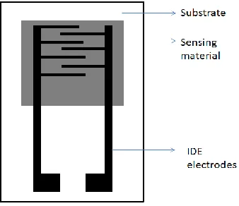
Fig. 2.1: Top view of a chemiresitor sensor showing the sensitive material and
interdigitated electrodes (IDE) on a silicon substrate. ………. 9
Fig. 2.2: Side view of metal oxide semiconductor sensor with a microheater unit. … 11
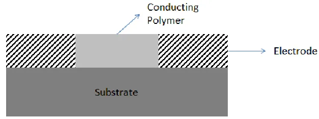
Fig. 2.3: Side view of conducting polymer sensor showing the employment of conducting polymer as the active sensing layer. ……….. 12
Fig. 2.4: Side view of carbon nanotube sensor showing the highly adsorptive carbon nanotube as the sensing material with the ohmmeter as the measurement unit. ……. 14
Fig. 2.5: Side view of quartz crystal microbalance sensor showing the quartz substrate sandwiched between two electrodes. ……… 16
Fig. 2.6: Top view of surface acoustic wave sensor showing the propagation a SAW waves across the sensing material from IDT. ………..… 18
Fig. 2.7: Side view of optical sensor showing the light propagating through fiber and getting modulated due to the interaction with target gas. ………...….. 19
Fig. 3.1: Quartz Crystal Microbalance Sensor (a) Top view of a quartz crystal microbalance sensor showing the top gold electrodes (b) Side view showing the quartz sandwiched between two gold electrodes. ……… 23
Fig. 3.2: Quartz crystal orientation (a) Quartz crystal (b) AT cut - crystal 350 15‟
degree to the z-axis……….. 23
Fig. 3.3: Quartz crystal microbalance sensor undergoing thickness shear mode of oscillation when AC current is applied. ………... 25
Fig. 3.4: Piezoelectric effect (a) Quartz crystal when no electric potential is applied (b) Quartz when electric potential is applied between its two electrodes and exhibiting inverse piezoelectric effect. ……… 25
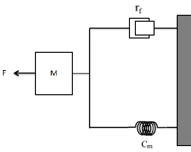
Fig. 3.5: Mechanical equivalent model of the quartz crystal microbalance…………. 29
Fig. 3.6: Electrical equivalent model of the quartz crystal microbalance without electrode contact. ………. 30
xiv
Fig. 4.1: Analytical modeling result presenting relationship between the resonant
frequency, f0, and the thickness of quartz substrate, tq. ……….. 34
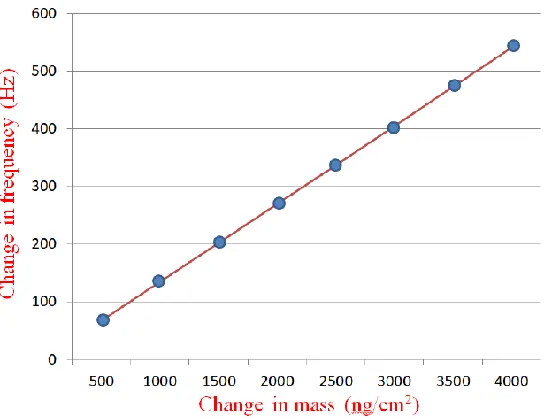
Fig. 4.2: Analytical modeling result presenting the linear relationship between the
mass and frequency with a sensitivity of 0.135 ng. cm-2. Hz-1………. 36
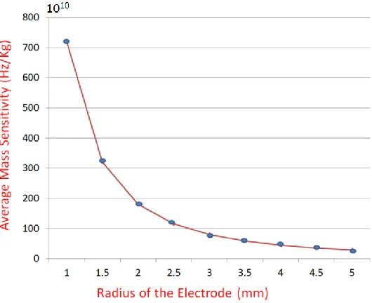
Fig. 4.3: Analytical modeling result presenting relationship between the average mass sensitivity (Δf/Δm) and radius of the electrode (mm) for a 5MHz quartz crystal microbalance sensor. ……… 37
Fig. 4.4: Analytical modeling result presenting relationship between the average mass sensitivity (Δf/Δm) and radius of the electrode (mm) for a 10 MHz quartz crystal microbalance sensor……….. 37
Fig. 4.5: COMSOL simulation results showing the resonant frequency characteristics to analyze the meshing characteristics (a) Normal mesh (b) Fine mesh (c) Finer mesh (d) Extra fine mesh. ……… 41
Fig. 4.6: COMSOL simulation results illustrating the effect of meshing on the output resonant frequency………. 42
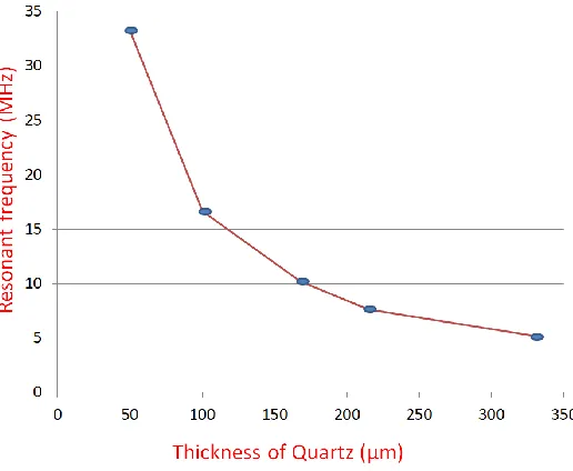
Fig. 4.7: COMSOL simulation results showing the resonant frequency characteristics to analyze the thickness of quartz crystal (a) 50μm (b) 100μm (c) 168μm (d) 215μm (e) 333μm……… 44
Fig. 4.8: COMSOL simulation results illustrating the relationship between the resonant frequency and the thickness of quartz (μm) ……….…. 45
Fig. 4.9: COMSOL simulation results showing the resonant frequency characteristics to analyze the radius of quartz crystal (a) 500μm (b) 750μm (c) 1mm (d) 2mm (e) 3mm (f) 7mm……… 47
Fig. 4.10: COMSOL simulation results illustrating the relationship between the resonant frequency and the radius of quartz (μm) ……….….. 48
Fig. 4.11: COMSOL simulation results showing the resonant frequency characteristics to analyze the thickness of gold electrodes (a) 50nm (b) 200nm (c) 300nm (d) 400nm (e) 500nm (f) 1000nm……….…… 49
Fig. 4.12: COMSOL simulation results illustrating the relationship between the displacement and the thickness of gold electrode (nm) ………..…….
xv
Fig. 4.13: COMSOL simulation results showing the resonant frequency characteristics to analyze the radius of gold electrodes (a) 100μm (b) 300μm (c) 1mm (d) 3mm………... 51
Fig. 4.14: COMSOL simulation results illustrating the relationship between the resonant frequency and the radius of gold electrode for the 5MHz range……… 52
Fig. 4.15: COMSOL simulation results illustrating the relationship between the resonant frequency and the radius of gold electrode for the 10MHz range…………. 52
Fig. 5.1: Conventional circular electrode (a) Geometry - Radius of quartz (RQ) – 12mm, Radius of electrode (RE) – 4.25mm (b) Displacement profile along the electrode axis of RE – 4.25mm (c) 2D plot of displacement profile exhibiting Gaussian curve……….. 58
Fig. 5.2: Ring electrode (a) Geometry - Radius of quartz (RQ) – 12mm, Radius of electrode (RE) – 4.25mm, Ring width (RW) – 2.125mm (b) Displacement profile along the electrode axis with RW – 2.125mm (c) Geometry - Radius of quartz (RQ) – 12mm, Radius of electrode (RE) – 4.25mm, Ring width (RW) – 1mm (d) Displacement profile along the electrode axis with RW – 1mm……….…. 59
Fig. 5.3: Ring dot electrode (a) Geometry - Radius of quartz (RQ) – 12mm, Radius of electrode (RE) – 4.25mm, Ring width (RW) – 2.125mm with dot radius (RD) - 500μm (b) Displacement profile along the electrode axis with RW – 2.125mm (c) Geometry - Radius of quartz (RQ) – 12mm, Radius of electrode (RE) – 4.25mm, Ring width (RW) – 1mm with dot radius (RD) - 500μm (d) Displacement profile along the electrode axis with RW – 1mm………. 61
Fig. 5.4: Comparison of displacement profiles of circular, ring and ring dot electrodes. ……… 62
Fig. 5.5: Multiple ring electrode (a) Equal ring width (b) Displacement profile along the electrode axis with RE – 2.5mm (c) Ascending ring width (d) Displacement profile along the electrode axis with RE – 2.75mm.………..……….. 64
Fig. 5.6: Schematic illustration of the concentric circle electrode geometry with ascending ring width and equal gap. ………..……..
65
xvi
Fig. 5.8: Displacement profile of concentric electrodes (a) Ratio 1 [1:1:1.5:2] with C = 250μm (b) Ratio 1[1:1:1.5:2] with C = 500μm (c) Ratio 2 [1:0.5:1:2:3] with C = 250μm (d) Ratio 2 [1:0.5:1:2:3] with C = 500μm. ………... 67
Fig. 5.9: Schematic illustration of the concentric circle electrode geometry with ascending ring width and descending gap. ……….. 67
Fig. 5.10: Concentric electrode with ascending ring width and descending gap a) Geometry - Radius of quartz (RQ) – 12mm, Radius of electrode (RE) – 4.25mm, Ring width 1 (RW1) – 500μm, RW2 - 750μm and RW3 – 1mm with dot radius (RD) - 500μm, Gap 1 (G1) - 500μm, G2 - 350μm, G3 - 200μm b) Displacement profile along the electrode axis with RE – 3.8mm. ……….. 68
Fig. 5.11: Comparison of displacement profiles of conventional circular electrode and concentric electrode. ………. 69
Fig. 6.1: Design of un-etched multichannel QCM design in which c2c is the distance between the center to center of adjacent electrodes (a) Top view showing four concentric electrodes (b) Side view of the un-etched QCM array……… 72
Fig. 6.2: Multichannel un-etched QCM design in COMSOL (a) Top view showing the four concentric electrodes (b) Node point pattern in COMSOL for the un-etched QCM design.………. 73
Fig. 6.3: COMSOL results showing the resonant frequency characteristics in order to analyze the frequency interference in un-etched QCM array for (a) c2c = 1.25mm, Electrode Ⅰ, Ⅱ (b) c2c = 1.25mm, Electrode Ⅲ, Ⅳ (c) c2c = 2.5mm, Electrode Ⅰ, Ⅱ (d) c2c = 2.5mm, Electrode Ⅲ, Ⅳ (e) c2c = 5mm, Electrode Ⅰ, Ⅱ (f) c2c = 5mm, Electrode Ⅲ, Ⅳ (g) c2c = 6.5mm, Electrode Ⅰ, Ⅱ, Ⅲ, Ⅳ……… 74
Fig. 6.4: COMSOL results illustrating the resonant frequency on all four un-etched QCM channels versus center to center (c2c) distance between the electrodes – c2c distance 6.5mm provides zero cross talk. ……… 76
Fig. 6.5: Schematic illustration of the side view of dual inverted mesa QCM with concentric electrodes showing the significant parameters. ………. 78
xvii
Fig. 6.7: Node point pattern in COMSOL for a single channel high frequency dual inverted mesa QCM design.. ………... 81
Fig. 6.8: COMSOL simulation results showing the resonant frequency characteristics for various radius of quartz (RQ) (a) RQ = 0.75mm (b) RQ = 1mm (c) RQ = 1.5mm (d) RQ = 2mm………...… 82
Fig. 6.9: COMSOL simulation results illustrating the characteristics of resonant frequency versus the radius of quartz (RQ) in which RQ is observed to be constant from 2mm. ……… 83
Fig. 6.10: Node point pattern in COMSOL for the two channel high frequency dual inverted mesa QCM design………... 85
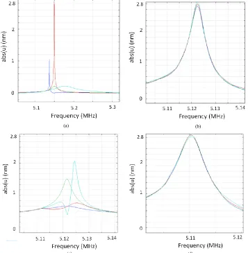
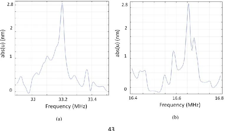
Fig. 6.11: COMSOL results showing the resonant frequency plot of the two 33.3MHz frequency channels which indicates the level of interference for various c2c values with NVT = 168μm. (a) c2c = 4.5mm (b) 6.5mm (c) 10mm (d) 15mm.… 85
Fig. 6.12: COMSOL results showing the resonant frequency plot of the two 33.3MHz frequency channels which indicates the level of interference for various c2c values with NVT=333μm. (a) c2c = 4.5mm (b) 6.5mm (c) 10mm (d) 13mm...… 86
Fig. 6.13: COMSOL results showing the resonant frequency plot of the two 10MHz frequency channels which indicates the level of interference for various c2c values with NVT = 333μm. (a) c2c = 4.5mm (b) 5.5mm (c) 6mm………. 88
Fig. 7.1: Schematic view of photolithography process to pattern the quartz etch area (a) deposition of photoresist on the quartz crystal (b) Alignment of mask and UV light exposure (c) patterned quartz crystal……… 92
Fig. 7.2: Schematic view of AT cut quartz etching process (a) Deep reactive ion etching process (b) Etched quartz with inverted mesa structures………. 93
Fig. 7.3: Schematic view of deposition of chromium and gold followed by the photolithography process to pattern the electrode area (a) deposition of chromium of 20nm and gold of 300nm (b) deposition of photoresist (c) Alignment of mask layer and exposure to UV light (d) Patterned gold layer……….. 95
Fig. 7.4: Schematic view of defining the top concentric electrodes (a) Using gold and chromium etchants, the exposed metallic layers are removed (b) Spray coating of photoresist on the top surface as a protective layer for further fabrication. ……… 95
xviii
on the inverted device (a) deposition of photoresist on the quartz crystal (b)
Alignment of mask and UV light exposure (c) patterned quartz crystal………. 96
Fig. 7.6: Schematic view of deep reactive ion etching process on the inverted device (a) etched quartz crystal (b) Removal of photoresist layer………... 97
Fig. 7.7: Schematic view of deposition of chromium and gold followed by the photolithography process to pattern the circular reference electrode (a) deposition of chromium of 20nm and gold of 300nm (b) Deposition of photoresist (c) Alignment of mask layer and exposure to UV light (d) Patterned gold layer on quartz………. 98
Fig. 7.8: Schematic view of formation of bottom circular electrodes (a) Using gold and chromium etchants, the exposed metallic layers are removed on the inverted quartz (b) Photoresist layers are removed by the developer solution………... 99
Fig. 7.9: Schematic view of dual inverted mesa quartz crystal microbalance sensor for 33.3MHz (a) Top view of the sensor showing four channels with concentric electrodes (b) Bottom view of the sensor showing four channels with circular reference electrodes. ……… 101
Fig. 7.10: Schematic view of dual inverted mesa quartz crystal microbalance sensor
xix
LIST OF ABBREVIATIONS/SYMBOLS
Abbreviation Explanation
VOC Volatile Organic Compounds
IDE Interdigitated Electrode
MOS Metal Oxide Semiconductor
CNT Carbon Nanotube
QCM Quartz Crystal Microbalance
SAW Surface Acoustic Wave
TSM Thickness Shear Mode
c2c Centre to Centre Distance
VT Vibrating Layer Thickness
NVT Non Vibrating Layer Thickness
RQ Radius of Quartz
RE Radius of Electrode
RW Ring Width
1
CHAPTER 1
INTRODUCTION
1.1 Motivation
Cancer is considered to be the second leading cause of death in the world, next to
heart disease [1]. It is defined as the spontaneous mutation in the single human body cells
to undergo multiple cell division which results in the formation of tumor [2]. This
mutation might be caused due to the environmental induced long or short term exposure
to cancer causing agents or genetic disorders [3]. There are more than hundred types of
cancer present which are characterized by the abnormal growth of the cells in the various
parts of the human anatomical system. Out of these several types of cancer, lung cancer is
one of the most common cancer with the highest number of cases of over 2 million
patients, which accounts for about 12.3% of the total cancer cases diagnosed in the year
2018 [4].
Lung cancer accounts for about 1.76 million death in 2018, which is the highest
mortality rate in the cancer related death [5]. This can be due to the late diagnosis of lung
cancer i.e. stage Ⅳ - cancerous cells have reached an abnormal growth and spread across
other organs in the human body [6]. According to the world health organization (WHO),
lung cancer patients diagnosed at the later stages are extremely hard to treat for the
oncologist as the cancerous cells fail to respond to the chemotherapy treatment at later
stages [7]. This late diagnosis of lung cancer limits the probability of curing the disease
and extending the life expectancy of the patients. If lung cancer is detected at an early
stage, there is a higher probability of survival, less expensive treatment and an increased
2
Early diagnosis of lung cancer is considered to be onerous and complicated as the
lung cancer patient at the early stages shows no symptoms or very less symptoms [9].
Conventional medical check-up such as chest X-ray does not recognise the lung cancer at
the initial stages while the highly advanced diagnosis techniques such as the computer
tomography (CT) [10], magnetic resonance imaging (MRI) [10], positron emission
tomography (PET) [10] scans are quite expensive and other medical techniques such as
sputum cytology [11] and biopsy are prescribed by the doctors only after the symptoms
shown during later stages of lung cancer.
During the early stages, the lung cancer patients exhales traceable amount of
volatile organic compounds (VOCs) in their breath in the range of 10 – 200 ppm whereas
a person without lung cancer has only 10 - 500 ppb range [12-14]. An alternative
diagnostic tool is proposed to effectively detect these small concentrations of VOCs in
the breath of the lung cancer patient. These proposed highly sensitive gas sensor arrays,
which are comparatively cheaper and faster than the conventional diagnosis methods, can
offer a higher probability of curing the lung cancer disease in a wide range scale [15-18].
In short, this volatile - detecting sensor should as affordable as a stethoscope and
effective as a CT scan so that even a general family doctor could use this gas sensor to
detect early signs of lung cancer in the patients.
1.2 Thesis Contribution
This research focuses on the design and development of quartz crystal
microbalance gas sensor array to analyze its critical design parameters and improve the
overall mass sensitivity of the device as well as to eliminate the interference between
3
In this thesis, several gas sensors are studied and analyzed for their capability in
the volatiles detection with necessary qualities such as the high sensitivity, selectivity,
reversibility, multiple target detection, low cost, ease of fabrication and smaller size.
From this baseline study, each sensor showcased their own advantages and
disadvantages, out of which the quartz crystal microbalance gas sensor is selected due to
its simple structure, which makes the fabrication process less complicated and less
expensive than the other gas sensors without compromising its performance in terms of
sensitivity and selectivity. This sensor also exhibits properties such as ability to detect
multiple gas targets in an array form and stability at higher temperature, which makes it a
suitable candidate for detecting the volatile organic compounds.
Accordingly, the principle of operation of the quartz crystal microbalance sensor
is studied and analyzed to investigate its potential for the necessary qualities. Following
this, the mass and frequency change relationship in the sensor are examined which forms
the basic working principle of this gas sensor. A comprehensive analytical modelling on
the resonant frequency characteristics has shown its major relationship with the thickness
of the quartz substrate. Furthermore, analytical modelling has been done on the mass
sensitivity of the device by altering the significant parameters such as the radius of
electrode which serves as a critical candidate in deciding the mass loading area and
understanding the energy trapping effect of the quartz crystal.
Moreover, the standard analytical modelling cannot withstand variations in the
electrode size, structure or the material used. Thus, in order to verify the analytical
modelled results and to extract the optimised critical design parameters, finite element
4
determined the optimal value for the significant design parameters such as the thickness
and radius of the quartz and gold electrode and their interlink with the resonant frequency
characteristics of the device. Investigation on the electrode structures are carried out
through finite element analysis which exposed its relationship between the distribution of
the sensitivity and the electrode depending on its structure. Comparison between the
classic circular electrodes and the ring electrodes are studied and analyzed to improve the
electrode structure.
Furthermore, a novel design of electrode structure called as the concentric
electrodes is proposed in order to overcome the uneven mass sensitivity distribution
limitations in the standard electrode structures such as the circular and ring electrodes. In
this new design, there are two main parameters that are significant for the higher
sensitivity such as the width of the rings and the gap between the rings which are altered
with the finite element analysis to provide an approximate uniform mass sensitivity
distribution. Then, these customized electrodes are designed and placed in an array.
Two types of array have been proposed which are the un-etched and etched
monolithic quartz crystal microbalance (QCM) arrays. The un-etched monolithic QCM
array has a 5MHz fundamental frequency of operation while the etched monolithic QCM
array has a 10MHz and 33MHz fundamental frequency of operation. Array configuration
produces frequency interference between the channels. Therefore, in order to eliminate
the frequency interferences, the distance between the electrodes are altered and the dual
inverted mesa structures are introduced. Finally, in order to fabricate the proposed quartz
5
procedures are investigated and a feasible process procedure to fabricate the device is
proposed.
1.3 Thesis Outline
In Chapter 2, various types of gas sensors are investigated based on their detecting
mechanism. Their advantages and disadvantages are reviewed to eventually find the
optimal gas sensor with the necessary qualities.
Chapter 3 is the detailed study of the principle of operation of the quartz crystal
microbalance gas sensor and its working mechanism. The frequency and mass change
interrelation and the piezoelectric effect are studied.
Following this, comprehensive analytical modelling and finite element analysis
has been done in the Chapter 4. The resonant frequency characteristics of the proposed
quartz crystal sensors are theoretically analyzed and the mass sensitivity relationship with
the size of the electrode are investigated using Sauerbrey‟s equation followed by the
investigation of the critical design parameters of the proposed device such as the radius
and thickness of quartz and gold in order to determine their relationship with device
overall performance with the finite element analysis.
Chapter 5 presents the study and analysis of the device electrode structures and
their relationship with the mass sensitivity of the proposed device along with the
comparison between the conventional circular electrode and the ring electrode. A novel
design of the electrode structure called as the concentric electrode is proposed. The
significant design parameters of the proposed electrode which determine the efficiency of
the sensor are investigated and optimised through the finite element analysis. Their
6
Chapter 6 presents the monolithic multiple electrode design of the quartz crystal
microbalance sensor in an array configuration. Two types of monolithic QCM arrays are
proposed in this chapter. In order to eliminate the frequency interference in the array,
finite element analyses are conducted and the following simulation results are used to
develop an optimal configuration and distance between the electrodes in the array.
Furthermore, in order to reduce the size of high frequency QCM array, dual inverted
mesa structures are proposed and the critical design parameters are analyzed and
optimized.
Chapter 7 presents the fabrication process steps of the proposed sensor. The
fabrication steps are aimed to be less complicated as possible compared to the other gas
sensors to manufacture the device easily without compromising the performance.
Finally, Chapter 8 summarizes the work done in the thesis along with the
significant results obtained through this research. Then potential future works that can
improve the overall efficiency such as the addition of suitable sensing layer depending on
7
CHAPTER 2
GAS SENSOR TECHNOLOGY
Gas sensing technology has played a major role for several decades in many
medical, safety and detecting applications such as food quality detection [19], chemical
vapor detection [20], air quality monitoring [21], space exploration applications [22] and
electronic noses [23]. Several types of gas sensors are commercially available for
detecting volatile organic compounds depending upon the concentration and type of
volatiles. These types of gas sensors are categorized based on their detecting mechanism
which are further reviewed, investigated, and analyzed in this chapter.
2.1 Introduction
Gas sensors are commonly categorized based on their detecting mechanisms. The
functionality of majority of gas sensors depends on the electrical characteristic variation
such as the resistance [24] and capacitance [25] or the frequency variation [26] to detect
the target gas. These significant measurement variations are caused due to the fact that if
a target gas comes into contact with the sensor then a critical parameter undergoes
variation in the sensor which can be further mapped to detect the concentration or
presence of the target gas [27]. The efficiency of the gas sensor is measured in terms of
the sensitivity, selectivity, reversibility, accuracy, range of detection, recovery time and
the response time [28-30]. Multiple channels in a gas sensors is useful to detect multiple
gas target simultaneously and it is a significant quality in gas sensing because an array of
sensors can provide high accuracy in the detection compared to the single channel gas
8
The qualities of an ideal gas sensor for sensing multiple volatile gas targets are listed
below,
1. Ability to provide high sensitivity towards volatile organic compounds.
2. Possibility for design modification to detect multiple target volatile organic
compounds simultaneously.
3. Diverse sensing materials compatibility.
4. Simple design geometry and ease of fabrication.
5. High reversibility and reproducibility.
6. Comparatively robust design.
7. Miniaturized structure and low of cost.
The above qualities have the potential to provide a robust candidate sensor for
complex environment gas detection and the sensors that carry such qualities will be
investigated in this chapter.
2.2 Sensors Based on Electrical Variations
2.2.1 Chemiresistor Sensor
Chemiresistor sensor operates based on the variation in the resistance of the
sensor when the target gas comes into contact with the sensing material. Conventional
chemiresistor sensor geometry includes interdigitated electrodes (IDE), and a sensing
material that is deposited on the active surface of the sensor embedded on a silicon
substrate. The electrical variation occurs when the sensor comes into contact with the
target gas, which forms the basic working principle of the sensor as shown in the Figure
2.1 [31]. When the target gas comes into contact with the sensing material, the physical
9
changes, which as a result increases or decreases the resistance of the sensing material.
This change in the resistance are then measured to detect the concentration or presence of
the target gas by connecting the two electrodes to an external data processing unit to
analyze the physical and chemical changes in the sensing film. The chemiresistor can
employ a wide range of sensing material which further determines the properties of the
sensor such as the reversibility and lifetime [32].
Fig. 2.1: Top view of a chemiresitor sensor showing the sensitive material and interdigitated electrodes (IDE) on a silicon substrate.
Chemiresistor sensors are built with the simplest structural configuration among
the gas sensors. The chemiresistor sensors are fabricated with the sensitive material
bridging the gap between the two electrodes which is mounted on the silicon substrate.
The electrodes are usually made of gold or chromium for their high conductive and
inertness property. The sensing material is responsible for the conductance between the
electrodes. Owing to their simple geometry, they are highly preferred in the food aroma
sensing and industrial applications. They also benefit from the wide range of sensing
materials such as conducting and non-conducting polymers, grapheme, nanoparticles and
10
Although possessing wide range of advantages such as the high sensitivity, ease
of fabrication, wide ranges of available sensing materials, chemiresistor sensor lacks
selectivity and they are highly sensitive towards humidity and temperature present in the
environment [34]. Furthermore, they also have low selectivity in the detection of target
gases depending on the choice of sensitive materials such as polymers.
2.2.2 Metal Oxide Semiconductor Sensor
Metal oxide semiconductor (MOS) sensors are a different version of the common
chemiresistor sensor with a micro heater unit and the metal oxides as their sensing
materials. They are preferred for their accuracy rate, long lifetime, short response time
and easy integrations in electronic circuits. The working mechanism of the sensor
depends on the change of conductance when the reducing or oxidizing gas comes into
contact with the sensing material as shown in the Figure 2.2. This interaction changes the
physical and chemical properties of the sensing material which forms the basis of this
sensor [35]. Each metal oxide sensing materials are sensitive to a particular gas at a
suitable temperature. This suitable optimum temperature can be provided by an
electrically separated micro heater unit which heats the metal oxides and makes the
sensing material reactive to various gas targets as per the requirement. The MOS sensing
material can be classified into n-type and p-type materials [36]. Some of the n-type metal
oxides are TiO2, ZnO, SnO2 and WO3 and p-type metal oxides are NiO, Mn3O4 and Cr2O3. The majority charge carriers in the type MOS are electrons. The reactivity of n-type MOS with reducing gas increases the conductivity and its reactivity with the
oxidizing gas increases the conductivity. Whereas, the majority charge carriers in the
11
conductivity and the its reactivity with the oxidizing gas decreases the conductivity.
These changes in the conductivity are measured with an external circuit or signal
processing unit which forms the basic working principle of the sensor [37].
Fig. 2.2: Side view of metal oxide semiconductor sensor with a micro heater unit.
The metal oxide semiconductor gas sensors have a complex geometry due to the
integration of the micro heater unit which needs electrical isolation area in the design.
The sensor consists of two inter digitated electrodes (IDE) connected by the metal oxide
sensing material. The micro heater unit is placed below the substrate material in order to
have a full coverage for the heat. They are electrically isolated by an insulating layer with
high temperature tolerance. The device is commonly built on a silicon substrate.
Metal oxide semiconductor has advantages such as the measurement simplicity,
durability, low cost, long lifetime and a wide range of sensing materials. However they
have some practical limitations such as the higher power consumption of the micro heater
which limits the portable applications and the heating units are not always preferred in
the bio sensing applications. Although array configuration is possible with this sensor, the
heat dissipation on a large scale array is considerably difficult to manage [38-39].
12
The conducting polymer sensor are known for their wide range of available active
sensing materials such as the polypyrrole (PPy), polyaniline (Pani), polythiophene (PTh)
and their derivatives [40]. Conducting polymer sensors have many advantages such as the
high sensitivity, simple design, short response time and stability at room temperature.
However, they are sensitive to temperature changes and humidity. The conducting
polymers possess fine mechanical properties which makes the fabrication of the polymer
sensor process much easier than its competitive gas sensors as shown in the Figure 2.3.
When the gas target gas comes into contact with the sensing polymer, the change in the
doping levels occurs. The doping levels of the conducting polymers strongly depend on
the chemical reaction with chemical gas. This interaction either dope or undope the
sensing material which alters the conductance of the material. This change in electrical
property is measured which forms the basic working principle of this sensor [41].
Fig. 2.3: Side view of conducting polymer sensor showing the employment of conducting polymer as the active sensing layer.
The polymer sensor consists of two electrodes usually made up of the gold for
their high conductance and inertness properties which are interconnected with the
polymer derivatives. The polymer material forms the active sensing layer. These
conducting polymers can be synthesized either through the chemical or electrochemical
13
polymers are fabricated in the silicon substrate. In some cases, in order to improve the
performance of electrical conductivity, inter digitated electrodes are employed [42].
Conducting polymers sensor has several advantages such as the high sensitivity,
wide range of available polymers and short response time [43]. Nevertheless, they have
some disadvantages including their sensitivity to the temperature and humidity [44], poor
reversibility and they not suitable for array configuration as the sensor occupies large
space [45].
2.2.4 Carbon Nanotubes Sensor
Carbon nanotubes are known for their extremely high adsorptive capacity even up
to an atomic level which is considered as the significant reason for its excellent
sensitivity and the popularity of the sensor [46]. Carbon nanotubes (CNT) possess several
characteristics such as the high strength, large electrical and thermal conductivity, and
high surface to volume ratios. These physical properties of the CNT provide smaller
dimensions for the overall size and higher electrical sensitivity for the sensor. CNT are
utilised in various types of sensors such as the resistive, capacitive and resonant
frequency change sensors [47]. However, the resistive type of measurement is the most
used sensor with CNTs owing to their simple geometry as shown in the Figure 2.4. The
interaction between the CNT and the target gas causes changes in the physical properties
of the CNT such as increase in the mass which subsequently increases the resistance and
decreases the conductance. CNT sensor uses conductance as the measurable variable.
This change in the electrical current can be measured which forms the basic working
14
Fig. 2.4: Side view of carbon nanotube sensor showing the highly adsorptive carbon nanotube as the sensing matrial with the ohmmeter as the measurement unit.
The carbon nanotubes can be either single walled or multi walled with varying
band gaps which act as semiconducting structures. The design of the CNT sensor is more
similar to the MOS gas sensor. The carbon nanotube sensors consist of electrodes bridged
by the carbon nanotubes which act as the active sensing layer. The source and drain
electrodes are connected by this CNT while the gate is insulated by the dielectric barrier
layer such as the silicon dioxide layer built on the silicon substrate [49].
Carbon nanotube sensor has several advantages such as the high sensitivity, great
adsorptive capacity. However, they have disadvantages such as the high in cost, complex
procedures to synthesise the carbon nanotube, fabrication complexity, long recovery
time, possible irreversible changes of carbon nanotube conductivity, poor selectivity and
they are also sensitive to the ambient conditions such as the presence of humidity and gas
flow rate [50].
2.3 Sensors Based on Acoustic Variations
2.3.1 Quartz Crystal Microbalance Sensor
The quartz crystal microbalance (QCM) sensor consists of AT cut quartz substrate
15
while the bottom electrode is grounded. Electrodes are usually made of gold or silver
while chromium is used as the adhesive layer for the electrodes and substrate. Gold is
mostly preferred as the electrode material due to its high conductivity and inertness
property. Due to its simple design, it has high potential for alterations in the design and
has the possibility to detect multiple gas targets simultaneously in the array configuration
[51].
Quartz crystal microbalance sensor is a mass sensitive device, which can detect
nanogram level of mass changes. Therefore, it is a preferred candidate sensor for various
fields of applications where there is a need for detection of target gases at low
concentration levels [52]. They are also preferred in the practical applications due to their
simple geometry and low cost of fabrication without compromising its performance in
sensing the gases. Due to their simple structure and geometry, the design modifications
are quite easy as per the demand in complex multiple gas sensing applications as shown
in the Figure 2.5. The quartz crystal microbalance depends on the piezoelectric property
of the quartz substrate [53]. The piezoelectric effect of the quartz can be defined as the
accumulation of charges in the surface of quartz crystal when they are subjected to
physical or mechanical stress. This voltage produced is proportional to the amount of
mechanical or electrical stress produced. In turn, when an AC electric potential is applied
across the quartz crystal, a mechanical deformation is produced and the crystal undergoes
thickness shear mode of oscillation at the resonant frequency. Any mass changes in the
electrically active area during the oscillation produce a direct shift in the resonant
16
measured with an impedance analyzer, which form the basic working principle of the
quartz crystal microbalance sensor [55].
Fig. 2.5: Side view of quartz crystal microbalance sensor showing the quartz substrate sandwiched between two electrodes.
The quartz crystal microbalance has several advantages in the case of volatile
detection such as the high sensitivity, wide range of sensing materials, potential to detect
multiple targets, simple geometry and ease of fabrication and reversibility depending on
the sensing material and high selectivity. Some of the sensing materials such as the
carbon nanotube, if used on the QCM sensor could result in sensitivity towards
temperature and humidity [56]. Although the conventional QCM operates with single
channel limiting its ability, design alterations are proposed to be made to operate in array
configurations as it will be investigate in Chapter 6 of this thesis.
2.3.2 Surface Acoustic Wave Sensor
The Surface Acoustic Wave (SAW) gas sensor is made up of interdigitated gold
transducers placed on the piezoelectric substrate. For the chemical and biological sensing
applications, the appropriate sensing material such as the polymer, carbon nanotube and
the metal oxides are coated on the surface layer which undergoes changes in the form of
17
Surface acoustic wave (SAW) sensors are widely popular for their high sensitivity in gas
applications and its ability to work in wireless modes. Such competitive advantages had
received continuous research and technological attention for the SAW gas sensor [58].
The SAW gas sensor depends on the variations in the SAW during the
propagation of the acoustic wave through the target gas. These variations are directly
proportional to the concentration of the target gas in the sensing region of the SAW
sensor. Initially, the surface acoustic waves are produced the interdigitated transducers
implanted on the piezoelectric material. These surface acoustic waves travel through the
surface region of the piezoelectric material depending on the order of the wavelength and
are detected by the receiver interdigitated transducer as shown in the Figure 2.6. Surface
acoustic wave undergoes change in either phase or frequency when they are interacted by
the corresponding gas targets. These changes can be accurately measured with impedance
analyzer or can be wirelessly received and processed which is the basic working principle
behind this sensor [59]. There are three stages in the operation of the SAW gas sensor,
i. Excitation of the piezoelectric substrate with the interdigitated transducer (IDT) to
produce acoustic waves.
ii. Acoustic waves undergoing modulation due to their interaction with the target
gases.
18
Fig. 2.6: Top view of surface acoustic wave sensor showing the propagation a SAW waves across the sensing material from IDT.
The surface acoustic wave sensor has advantages such as the high sensitivity,
excellent response time, smaller size, wireless mode of operation, and planar structure.
Although possessing such high advantages, it is inevitable for disadvantages such as the
complexity in the fabrication process and its difficulty to operate in an array
configuration that is a requirement for gas detection in a complex environment. Array
configuration ability is significant to detect multiple gas targets. The main difficulty in
the design for an array configuration with SAW sensor is the process of reducing the size
of the sensor comparative to the other competitive sensors such as the quartz crystal
microbalance which can provide the similar performance without design complications.
[60].
2.4 Sensors Based on Optical and Calorimetric Variations
2.4.1 Optical Sensor
The optical sensor consists of fiber optic cable with source of the light beam on
one side and the receiver of the light on the other side. The source of the light is usually
19
The cladding of the fiber cable is coated with the sensing material. The whole optic fiber
setup is fabricated on the silicon substrate as shown in the Figure 2.7 [61].
Optical sensors are widely known for their high sensitivity in the gas sensing
applications. The accuracy of the optical sensors is comparatively better than other
competitive sensors. These fiber optic gas sensors depend on the pulse width modulation
of the source light for sensing the target gas concentration [62]. Initially the beam of light
is passed through the fiber optic from the source which is modulated by the interaction
with the chemical gases. This modulation causes variations in the physical properties of
the source white light beam which is measured at the receiver end through a photo voltaic
reader. The refractive index of the source beam changes when an adsorption or scattering
occurs due to interaction. This measured variation in the refractive index of the pulse
width modulation is directly proportional to the concentration of the chemical gas
detected at the sensing region. The sensitivity can be increased by employing the
appropriate sensing materials [63].
Fig. 2.7: Side view of optical sensor showing the light propagating through fiber and getting modulated due to the interaction with target gas.
The optical sensor has several advantages such as the high sensitivity, accuracy of
20
expensive setup and its difficulty to work in an array configuration for multiple targets
detection simultaneously. Despite having several advantages, the optical sensors are not
preferred in the volatile detection because of the difficulty in miniaturization and
difficulty in array configuration setup [64].
2.4.2 Calorimetric Sensor
The calorimetric sensor has several chemi-adsorptive dyes implanted which turns
colour when the target gas comes into contact with the sensing layer of the sensor. This
interaction between the chemi-adsorptive dye and the gas undergoes chemical process
and the colour of the dye changes. This change in the colour is further detected and
calculated with a suitable image processing system and the presence of the target gas is
detected. The calorimetric sensors are the most low cost gas sensor for the volatile
detection and they work in an array configuration.
The calorimetric sensor some advantages such as the low cost, ability to work in
array configuration and stability. However, it has disadvantages such as the irreversibility
of the sensor response, long response time, low accuracy, high image processing power
[65].
2.5 Conclusion
From a comprehensive analysis of the commercial and common gas sensors, the
advantages and disadvantages of each individual sensor are analyzed and interpreted.
This interpretation determines that there are various gas sensors which can be used to
detect the volatiles. However, there are certain quality requirements specifically for
complex environment applications in the sensor performances. Among all the
21
advantages over the other sensors such as its high sensitivity, reversibility, selectivity,
long lifetime, robustness, simple design, ease of fabrication, potential for array
configuration and low cost of fabrication. Thus, implementing this candidate sensor in an
array configuration could provide a platform to detect multiple gas targets
simultaneously. Since QCM exhibited most of the required qualities and potential, the
focus of this thesis is on the design and development of high performance QCM sensor in
22
CHAPTER 3
QUARTZ CRYSTAL MICROBALANCE SENSOR
3.1 Introduction
Quartz crystal microbalance sensor is one of the candidate technologies for gas
detection and has received a high attention in the research and development due to their
advantages during the recent decades [66]. The simplicity in the design of this sensor
combined with high potential qualities is one of the major reasons for this research focus.
As discussed in the previous chapter, this sensor provides a competitive advantage and
qualities over other gas sensors in its range such as the wide choice for the sensing
material, potential to detect multiple gas targets in array configuration and smaller size.
The working mechanism of the Quartz crystal microbalance sensor and its physics of
operation are discussed and investigated in detail in this chapter.
3.2 Basic Structure and Mechanism of Operation
3.2.1 Quartz Crystal Microbalance – Design Principle
The Quartz crystal microbalance sensor is commonly built on an AT cut quartz
crystal that usually has a thickness ranging between 330μm to 168μm as shown in the
Figure 3.1 depending on the need for resonant frequency. The AT cut of the quartz
crystal is achieved by cutting the quartz crystal 35° 15' degree to the principle optical axis
of the crystal (z-axis) as shown in the Figure 3.2 [67]. The quartz crystal that are found in
nature are rare and expensive, therefore, they are nowadays synthetically grown. These
crystals are subjected to various process such as annealing and electrical sweeping in
order to reduce the number of defects and impurities in the crystal, which may cause
23
their stability in operation and its temperature tolerance, which helps the device to
operate even at higher temperature without causing shift in the frequency. Quartz can
have piezoelectric effect even up to 573° C [69]. In a quartz crystal microbalance
structure, this AT cut quartz crystal is sandwiched between the two metallic electrodes in
order to apply the AC potential. In these devices, electrodes are usually made of gold,
titanium, silver or platinum however, gold is preferred for its high conductivity and
inertness property as it is chemically non-reactive. Although copper and silver are more
conductive than the gold, they do not possess inertness property similar to gold [70].
Fig. 3.1: Quartz crystal microbalance sensor (a) Top view of a quartz crystal microbalance sensor showing the top gold electrodes (b) Side view showing the quartz sandwiched between two gold electrodes.
Fig. 3.2: Quartz crystal orientation (a) Quartz crystal (b) AT cut - crystal 35 0 15 / degree to the
z-axis
(a) (b)
24
3.2.2 Thickness Shear Mode (TSM) Oscillation
Quartz is made up of silicon and oxygen bonds. These silicon and oxygen bonds
have a non-linear nature, which results in a net dipole moment in the quartz. When an
alternating current is applied across the metallic electrodes that are deposited on both
sides of the crystal, the opposite ends of the dipole tend to pushed in the opposite
directions followed by the dipoles tending to rotate themselves to be aligned along the
direction of the applied electric field [71]. This displacement results in a net strain. The
displacement in the dipoles of the quartz also varies with the electric field resulting in the
mechanical deformational of the quartz crystal. As a result, the acoustic shear waves are
launched in the direction perpendicular to the direction of the crystal from the either sides
of the crystal. When this alternating current supply is removed, the crystal comes back
into its original form from the deformed state due to the absence of strain in the crystal.
The AT cut of the quartz is responsible for the thickness shear mode of oscillation as
shown in the Figure 3.3. AT cut is mostly used in quartz-based applications because of its
exceptional frequency stability [72].
25
3.2.3 Piezoelectric Property of Quartz
The deformation of the quartz on the application of alternating current is the result
of inverse piezoelectric effect. Since quartz is a piezoelectric crystal, it exhibits
piezoelectric property which is the production of electric field in its surface when a
mechanical stress is induced [73]. The magnitude of the electric current produced is
directly proportional to the amount of stress applied on the crystal. Thus, inversely when
an electric current in an alternating form is applied between the top and bottom
electrodes, the quartz undergoes mechanical deformation in the form of an oscillation.
Inverse piezoelectric effect is the responsible for the thickness shear mode of oscillation
of the quartz crystal microbalance sensor [74].
Fig. 3.4: Piezoelectric effect (a) Quartz crystal when no electric potential is applied (b) Quartz when electric potential is applied between its two electrodes and exhibiting inverse piezoelectric effect.
3.2.4 Resonant Frequency
The frequency at which the piezoelectric quartz crystal undergoes thickness shear
mode of oscillation under the influence of applied alternating current (usually sine wave)
is called as the resonant frequency. This fundamental resonant frequency of the quartz is
used for sensing and acts as an indicator for the sensor exposure which undergoes
variations. It either increases or decreases by a certain level of Hz depending upon the
addition or removal of the mass on the surface of the electrically active sensing electrode
26
mass increases the resonant frequency. These variations in the resonant frequency can be
monitored with a high frequency oscillator. The relationship between the frequency and
mass in the quartz crystal microbalance was first observed by Sauerbrey, a German
physicist in 1959 and devised equations called as the Sauerbrey‟s equation of mass and
frequency relationship [76].
3.2.5 Sensitivity
The magnitude of variation in resonant frequency for a particular amount of mass
determines the sensitivity of the Quartz crystal microbalance sensor. In an ideal case,
Quartz crystal microbalance can detect up to 1ng amount of change in mass on its sensing
electrode surface. If the center resonant frequency of the quartz crystal microbalance is
higher, the sensor tends to be more sensitive towards the mass which results in a larger
shift in the resonant frequency compared to sensor with lower center resonant frequency
[77]. Although higher resonant frequency has advantage of more sensitivity, they are
fragile due to their thin quartz substrate compared to lower resonant frequency sensor that
uses comparatively thicker substrate [78].
3.3 Mass and Frequency Relationship
When an alternating current is applied on the metallic electrodes of a Quartz
crystal microbalance, the device starts to oscillate at the resonant frequency [79] which is
given by,
√
27
constant values, the resonant frequency is directly influenced by the thickness of the
quartz crystal.
This resonant frequency f0 of the quartz changes either by addition or removal of the mass on the electrically active sensing area. This mass and frequency relation is
devised in an equation by Sauerbrey,
where, A is the area of electrodes of the quartz crystal microbalance, Δf is the change in
the resonant frequency, Sc is the Sauerbrey constant equals to 2.264 × 10⁻⁶ g-1 cm-2 s and Δm is the change in mass on the surface of electrode. The negative sign denotes the
reduction in the resonant frequency by addition of mass on the top of electrode. The
Sauerbrey‟s equation of mass-frequency relationship is derived as follows:
where, mq is the mass per unit area and Mq is the total mass of the quartz crystal. This Equation 3.3 is combined with 3.1, to obtain,
√
By addition of some quantity of mass to the electrode causes change in the resonant
frequency which can be written as,
√
Equation 3.4 is substituted in the above equation 3.5, to obtain,
√
√