NOT
RECOMMENDED FOR
NEW DESIGNS
REFER T
O
MA702
with Side-Shaft Positioning Capability
DESCRIPTION
The MagAlpha MA700 is a robust, contactless, angle encoder. The IC detects the absolute angular position of a permanent magnet, typically a diametrically magnetized cylinder attached to the rotor. The data acquisition and processing is extremely fast, allowing accurate angle measurement at speeds from 0 to 100,000 RPM
The MA700 supports a wide range of magnetic field strengths and spatial configurations, which help to relax mechanical tolerances and simplify system design. Both end-of-shaft magnet and off axis magnet positioning (side-shaft mounting) topologies are supported.
Please See Position Sensor Design Support for All Supporting Software
FEATURES
11-Bit Resolution Absolute Angle Encoder 500kHz Refresh Rate
Ultra-Low Latency: 3µs
Serial Interface for Data Readout and settings
10-Bit Incremental Output (A, B, Z) Built-In Linearization for Side-Shaft
Mounting
3.3V, 7.7mA Supply
Available in a QFN-16 (3mmx3mm) Package
APPLICATIONS
Servo Drives Robotics Automotive PSM/BLDC Motors Encoders
All MPS parts are lead-free, halogen-free, and adhere to the RoHS directive. For MPS green status, please visit the MPS website under Quality Assurance. “MPS” and “The Future of Analog IC Technology” are registered trademarks of Monolithic Power Systems, Inc.
NOT
RECOMMENDED FOR
NEW DESIGNS
REFER T
O
MA702
MA700 Rev. 1.3 www.MonolithicPower.com 2
7/3/2018 MPS Proprietary Information. Patent Protected. Unauthorized Photocopy and Duplication Prohibited. © 2018 MPS. All Rights Reserved.
ORDERING INFORMATION
Part Number* Package Top Marking
MA700GQ QFN-16 (3mmx3mm) See Below
* For Tape & Reel, add suffix –Z (e.g. MA700GQ–Z)
TOP MARKING
y: Year code O: Optional marking LLL: Lot number
PACKAGE REFERENCE
TOP VIEWNOT
RECOMMENDED FOR
NEW DESIGNS
REFER T
O
MA702
ABSOLUTE MAXIMUM RATINGS
(1)Supply voltage (continuous) ... -0.5V to +3.8V Supply voltage short term ... -0.5V to +4.1V I/O pin voltage ... -0.5V to 3.8V Continuous power dissipation (TA = +25°C)
(2)
... 2.5W
Thermal Resistance
(3)θ
JAθ
JCQFN-16 (3mmx3mm)...50 ... 12 ... °C/W
NOTES:
1) Exceeding these ratings may damage the device.
2) The maximum allowable power dissipation is a function of the maximum junction temperature TJ (MAX), the
junction-to-ambient thermal resistance θJA, and the ambient temperature
TA. The maximum allowable continuous power dissipation at
any ambient temperature is calculated by PD (MAX) = (TJ
(MAX)-TA)/θJA.
NOT
RECOMMENDED FOR
NEW DESIGNS
REFER T
O
MA702
MA700 Rev. 1.3 www.MonolithicPower.com 4
7/3/2018 MPS Proprietary Information. Patent Protected. Unauthorized Photocopy and Duplication Prohibited. © 2018 MPS. All Rights Reserved.
ELECTRICAL CHARACTERISTICS
Parameter Symbol Condition Min Typ Max Units
Operating Conditions
Supply voltage VDD 3.0 3.3 3.6 V
Supply voltage for OTP
flashing Vflash 3.9 4.0 4.1 V
Supply current for OTP
flashing (4) Iflash 50 100 mA
Operating temperature Top -40 125 °C
Applied magnetic field B 30 75 mT
NOTE:
NOT
RECOMMENDED FOR
NEW DESIGNS
REFER T
O
MA702
ELECTRICAL CHARACTERISTICS
VDD = 3.3V, 50mT < B < 100mT, temp = -40°C to+125°C, unless otherwise noted.
Parameter Symbol Condition Min Typ Max Units
Sensor Output Specifications
Power-up time (5) 2 3 ms
Supply current 6.0 7.7 8.8 mA
INL at 25°C At room temperature over
the field range ±0.9 ±1.6 ±2.0 deg
INL between -40°C to +125°C (5)
The largest value over the temperature range and field range
±0.5 ±1.6 ±2.5 deg
Output Drift
Temperature induced (5) -0.026 +0.026 deg/°C
Magnetic field induced (5) -0.023 +0.023 deg/mT
Voltage supply induced (5) -0.7 +0.7 deg/V
Absolute Output – Serial
Data output length 16 16 bit
Refresh rate 488 524 558 kHz
Latency (6) Measured at constant
speed 3 µs
Resolution (3σ noise level)
Measured by averaging
over all angles 10.7 12.0 13.0 bit
Incremental Output – ABZ (7)
Resolution 1024 edges/revol.
Pulses per channel 256 A or B/revol
Jitter Up to 15,000 RPM 10 % of a
period
Hysteresis (6) 0.2 0.27 deg
Digital I/O
Threshold voltage high 1.75 V
Threshold voltage low 1.05 V
Rising edge slew rate CL = 50pF 0.7 V/ns
Falling edge slew rate CL = 50pF 0.7 V/ns
OTP Flash Timing
Flashing time for one
register (6) 2.6 ms
Period for multiple registers flashing(6)
Time between 2 successive
flash commands 2.6 ms
NOTES:
5) Guaranteed by design.
6) Guaranteed by characteristic test. 7) See Appendix B.
NOT
RECOMMENDED FOR
NEW DESIGNS
REFER T
O
MA702
MA700 Rev. 1.3 www.MonolithicPower.com 6
7/3/2018 MPS Proprietary Information. Patent Protected. Unauthorized Photocopy and Duplication Prohibited. © 2018 MPS. All Rights Reserved.
TYPICAL CHARACTERISTICS
VDD = 3.3V, temp = 25°C, unless otherwise noted.
NOT
RECOMMENDED FOR
NEW DESIGNS
REFER T
O
MA702
PIN FUNCTIONS
PackagePin # Name Description
1, 9, 10,
11, 14, 15 NC No connection. Leave unconnected. 2 A Incremental output.
3 Z Incremental output.
4 MOSI Data in. Serial. 5 CS Chip select. Serial. 6 B Incremental output.
7 MISO Data out. Serial. 8 GND Ground.
12 SCLK Clock. Serial. 13 VDD 3.3V supply.
NOT
RECOMMENDED FOR
NEW DESIGNS
REFER T
O
MA702
MA700 Rev. 1.3 www.MonolithicPower.com 8
7/3/2018 MPS Proprietary Information. Patent Protected. Unauthorized Photocopy and Duplication Prohibited. © 2018 MPS. All Rights Reserved.
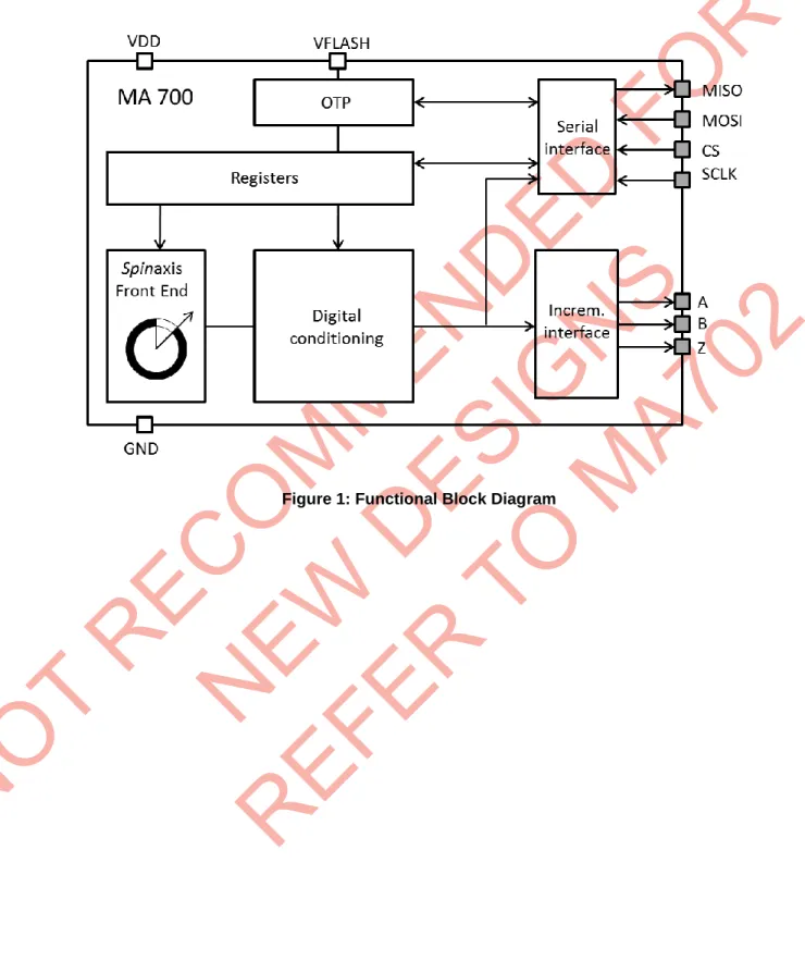
BLOCK DIAGRAM
NOT
RECOMMENDED FOR
NEW DESIGNS
REFER T
O
MA702
OPERATION
Timing of the Serial Interface
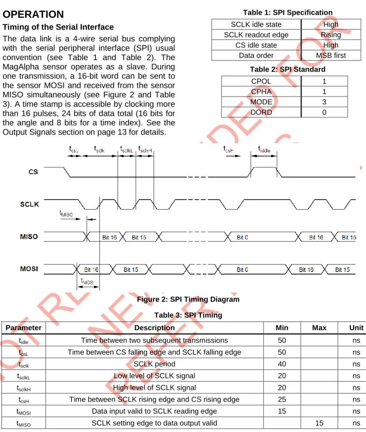
The data link is a 4-wire serial bus complying with the serial peripheral interface (SPI) usual convention (see Table 1 and Table 2). The MagAlpha sensor operates as a slave. During one transmission, a 16-bit word can be sent to the sensor MOSI and received from the sensor MISO simultaneously (see Figure 2 and Table 3). A time stamp is accessible by clocking more than 16 pulses, 24 bits of data total (16 bits for the angle and 8 bits for a time index). See the Output Signals section on page 13 for details.
Table 1: SPI Specification
SCLK idle state High
SCLK readout edge Rising
CS idle state High
Data order MSB first
Table 2: SPI Standard
CPOL 1
CPHA 1
MODE 3
DORD 0
Figure 2: SPI Timing Diagram Table 3: SPI Timing
Parameter Description Min Max Unit
tidle Time between two subsequent transmissions 50 ns
tcsL Time between CS falling edge and SCLK falling edge 50 ns
tsclk SCLK period 40 ns
tsclkL Low level of SCLK signal 20 ns
tsclkH High level of SCLK signal 20 ns
tcsH Time between SCLK rising edge and CS rising edge 25 ns
tMOSI Data input valid to SCLK reading edge 15 ns
NOT
RECOMMENDED FOR
NEW DESIGNS
REFER T
O
MA702
MA700 Rev. 1.3 www.MonolithicPower.com 10
7/3/2018 MPS Proprietary Information. Patent Protected. Unauthorized Photocopy and Duplication Prohibited. © 2018 MPS. All Rights Reserved.
REGISTERS
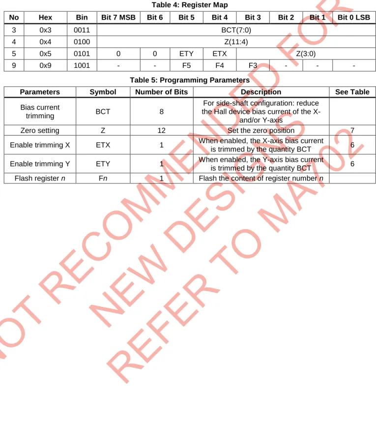
Table 4: Register Map
No Hex Bin Bit 7 MSB Bit 6 Bit 5 Bit 4 Bit 3 Bit 2 Bit 1 Bit 0 LSB
3 0x3 0011 BCT(7:0)
4 0x4 0100 Z(11:4)
5 0x5 0101 0 0 ETY ETX Z(3:0)
9 0x9 1001 - - F5 F4 F3 - -
-Table 5: Programming Parameters
Parameters Symbol Number of Bits Description See Table
Bias current
trimming BCT 8
For side-shaft configuration: reduce the Hall device bias current of the X-
and/or Y-axis
Zero setting Z 12 Set the zero position 7
Enable trimming X ETX 1 When enabled, the X-axis bias current
is trimmed by the quantity BCT 6
Enable trimming Y ETY 1 When enabled, the Y-axis bias current
is trimmed by the quantity BCT 6
NOT
RECOMMENDED FOR
NEW DESIGNS
REFER T
O
MA702
Sensor – Magnet Mounting
The sensitive volume of the MA700 is confined in a region less than 100µm wide and has multiple integrated Hall devices. This volume is located both horizontally and vertically within 50µm of the center of the QFN package. The sensor detects the angle of the magnetic field projected in a plane parallel to the package’s upper surface. This means that the only relevant magnetic field is the in-plane component (X and Y components) in the middle point of the package.
Rotation Direction
Looking at the MagAlpha from the top, the angle increases when the magnetic field rotates clockwise. Figure 3 shows the zero angle of the unprogrammed MA700, where the cross indicates the sensitive point.
Figure 3: Zero Angle of Unprogrammed MA700
This type of detection provides flexibility for the design of an angular encoder. The sensor only requires the magnetic vector to lie essentially within the sensor plane with an amplitude of at least 30mT. Note that the MA700 can work with fields smaller than 30mT, but the linearity and resolution performance may deviate from the specifications. The straightforward solution is to place the MA700 sensor on the rotation axis of a permanent magnet (i.e.: a diametrically magnetized cylinder) (see Figure 4).
If the end-of-shaft position is not available, the sensor can be positioned away from the rotation axis of a cylinder or ring magnet (see Figure 5). In this case, the magnetic field angle is no longer directly proportional to the mechanical angle. The MA700 can be adjusted to compensate for this effect and recover the linear relation between the mechanical angle and the sensor output. With multiple pole pair magnets, the MA700 can indicate multiple rotations for each mechanical turn.
Figure 5: Side-Shaft Mounting Mounting and Power Supply Decoupling
For most applications, a single 100nF bypass capacitor placed close to the supply pins decouples the MA700 from power supply noise. If better decoupling is required, a larger capacitor (i.e.: 1µF to 10µF) can be added in parallel with the 100nF capacitor, and/or a serial resistor (i.e.: 10Ω) can be added on the supply line. Ensure that the capacitor is connected with low impedance paths.
VFLASH needs to be supplied only when flashing the memory. Otherwise, VFLASH should remain unconnected (see Figure 6).
NOT
RECOMMENDED FOR
NEW DESIGNS
REFER T
O
MA702
MA700 Rev. 1.3 www.MonolithicPower.com 12
7/3/2018 MPS Proprietary Information. Patent Protected. Unauthorized Photocopy and Duplication Prohibited. © 2018 MPS. All Rights Reserved.
The exposed pad of the package can be soldered to the PCB to ensure optimum electrical, thermal, and mechanical conditions. In case the exposed pad is soldered, it is recommended that the pad be electrically connected to ground.
Sensor Front End
The magnetic field is detected with integrated Hall devices located in the center of the package. The angle is measured using the
Spinaxis method, which directly digitizes the direction of the field without any arctangent computation or feedback loop-based circuit (interpolators, etc.).
The Spinaxis method is based on phase detection. It requires sensitive circuitry that generates a sinusoidal signal with a phase that represents the angle of the magnetic field. The angle is then retrieved by a time-to-digital converter, which counts the time between the zero crossing of the sinusoidal signal and the edge of a constant waveform (see Figure 7). The digitized time is the front-end output. At the output, the front-end delivers a digital number proportional to the angle of the magnetic field at the rate of 500kHz in a straightforward and open-loop manner.
Top: Sine Waveform
Bottom: Clock of Time-to-Digital Converter
Figure 7: Phase Detection Method Side Shaft
In case the MA700 is mounted in a side-shaft configuration, the relationship between the field angle and the mechanical angle is no longer directly linear. This is related to the fact that the tangential magnetic field is usually smaller than the radial field.
The field ratio (k) can be defined with Equation (1):
tan
/B
B
k rad (1)
Where Brad is the maximum radial magnetic field,
and Btan is the maximum tangential magnetic
field (see Figure 8).
Figure 8: Side-Shaft Field
The ratio (k) depends on the magnet geometry and the distance to the sensor.
The X-axis or the Y-axis bias currents can be reduced to recover an equal Hall signal for all angles, and therefore suppress non-linearity. The parameters ETX and ETY control in which direction sensitivity is reduced. The current reduction is set by the parameter bias current trimming (BCT) (7:0), which is an integer from 0 to 255.
To find the optimum BCT, change the value until the non-linearity reaches a minimum. Such calibration should be performed on individual parts.
Sensor Orientation: ETX and ETY
The dot printed on the package shows whether the radial field is aligned with the sensor coordinate X or Y (see Figure 9).
Figure 9: Package Top View with X- and Y-Axes
First, determine which axis needs to be reduced (see the qualitative field distribution around in Figure 8). For instance, with the arrangement depicted in Figure 9, the field along Y is tangential and therefore weaker. The X-axis should be reduced (ETX = 1, ETY = 0). Note that if both ETX and ETY are set to 1, the current bias is reduced in both directions the same way (i.e.: without side-shaft correction) (see Table 6).
NOT
RECOMMENDED FOR
NEW DESIGNS
REFER T
O
MA702
Table 6: ETX and ETY
ETX Enable Trimming the X-axis
0 Disabled
1 Enabled
ETY Enable Trimming the Y-axis
0 Disabled
1 Enabled
Digital Signal Conditioning Digital Filtering
Advanced digital filtering improves the resolution without adding latency. Measuring the rotation speed over the last 256 data points in addition to the angular position provides the best possible evaluation of the present position with the smallest possible lag.
Zero Setting
The zero position of the MagAlpha (a
0) can be
programmed with 12 bits of resolution. The angle streamed out (a
out) can be calculated with
Equation (3):
0
a
a
a
out
fe
(3)Where a
fe is the raw angle out of the front end.
The parameter Z(11:0), which is 0 by default, determines a
0 (see Table 7). This setting is
valid for all output formats, such as SPI, ABZ, and UVW.
Table 7: Zero Position
Z(11:0) Zero Position a0 (deg)
0 0
1 0.088
… …
4095 359.912
Programming the MA700
The MA700 incorporates three programmable registers. Each register has 8 bits of memory. When the MA700 is powered up, each of these three 8 bits of memory are set to zero, unless the register was previously stored in the one-time programmable (OTP) memory. This means that during start-up, the content of the OTP memory is copied to the registers. Once flashed, the register content can no longer be modified. To set the content of a register, a digital stream must be sent to the register consisting of the
4-bit register/write command (0010), a 4-4-bit register address, and the 8-bit value.
The data stream, sent through the MOSI wire is a total of 16 bits long:
command reg.
address MSB value LSB 0 0 1 0
Once the command is sent, it is effective immediately and affects the next data sent from the MagAlpha.
Reading Back the Register Content
To check the content of a register to verify that the programming was successful, first send the register/read command (0001) and the 4-bit address of the register being tested. The last 8 bits of the stream are irrelevant. For instance, the value 0000 0000 can be sent:
command reg.
address MSB value LSB
0 0 0 1 x x x x x x x x
The MagAlpha response is within the same transmission. In the first byte (simultaneous to the 4-bit read command and the 4-bit address), the MagAlpha sends the 8 MSB of the measured angle A(15:8). The second byte is the content of the register being tested. After this transmission, the MagAlpha continues delivering the usual 16-bit angles A(15:0). For example, to check the content of the register 4 (0100), which contains 8 MSBs of the zero setting, send the data:
command reg.
address MSB value LSB 0 0 0 1 0 1 0 0 0 0 0 0 0 0 0 0
Simultaneously, the MagAlpha replies:
Angle out MSB value LSB
A(15:12) A(11:8) Z(7:0)
Output Signals
The bit order of the transmitted data is MSB first and LSB last. Every 2µs, new data is transferred into the output buffer. The master device connected to the MagAlpha triggers the reading by pulling CS down. When a CS signal falling edge occurs, the data remains in the output buffer until the CS signal returns to
NOT
RECOMMENDED FOR
NEW DESIGNS
REFER T
O
MA702
MA700 Rev. 1.3 www.MonolithicPower.com 14
7/3/2018 MPS Proprietary Information. Patent Protected. Unauthorized Photocopy and Duplication Prohibited. © 2018 MPS. All Rights Reserved.
the data by sending clock pulses with a maximum frequency of 25MHz. There is no minimum frequency or timeout. See Figure 10 for a simple reading of the 16-bit data.
Figure 10: Timing Diagram for Simple SPI Readout
A full reading requires 16 clock pulses. The MA700 delivers:
MSB LSB
A(15:8) A(7:0)
If less resolution is needed, the angle can be read by sending fewer than 16 pulses since the MSB is sent first. For instance, by sending only 8 pulses, the MagAlpha provides an 8-bit angle without ambiguity over 360 degrees:
MSB LSB A(15:8)
If the master triggers the reading faster than the refresh rate, the MagAlpha may send the same sample several times.
In some applications, it is helpful to know how many data updates occur between two successive readouts or if the same data points were read more than once. For this purpose, an 8-bit index attached to the data can be read. This keeps track of the precise time of measurement without needing to control the readout time precisely. This index runs from 0 to 255 and is incremented by 1 each time the output buffer is refreshed. The index can detect a double reading of the same data (same index) or show how many data points were skipped (see Figure 11).
To read the 8-bit index, the master must send 16 + 8 = 24 clock pulses.
Figure 11: Timing Diagram for SPI Angle + Index Readout
Incremental – ABZ
With the ABZ output, the MA700 emulates a 10-bit incremental encoder (such as an optical encoder) providing logic pulses in quadrature (see Figure 12). Compared to signal A, signal B is shifted by a quarter of the pulse period. Over one revolution, signal A pulses 256 times. This yields 1024 edges per revolution. Signal Z (zero or index) raises only once per turn at the zero-angle position. The minimum recommended field for ABZ reading is 35mT. See Appendix B for more information.
Figure 12: ABZ Output during Rotation
The ABZ state is updated every 2µs. This means that at a high RPM, an ABZ jitter is caused by the discretization of the pulse length. For instance, at 15,000 RPM, the period (P) of the signal A or B is 16µs. Therefore, the jitter is 2/16 = 12.5%. Note that the raising edge of Z occurs exactly at the sensor zero position. Due to the 1 LSB hysteresis introduced on both the A and B channels, the Z edge is not necessarily synchronized with an A or B edge (see Figure 13).
NOT
RECOMMENDED FOR
NEW DESIGNS
REFER T
O
MA702
Figure 13: ABZ Jitter
Above 15,000, the ABZ signal is still usable. Note that when the jitter is larger than 25% (i.e.: when the speed exceeds 30,000 RPM), the A and B signal edge may coincide.
One-Time Programmable (OTP) Programming
The one-time programmable (OTP) memory can permanently store the content of the programmable registers. The OTP memory is made of poly-silicon fuses. By activating the flash command, the content of an entire register can be stored in the OTP memory. The flash command consists of setting some bits (Fn, where n is the register number) in register 9. For flashing the register, when the bit Fn is set, the register n is stored permanently. It is important to note that only one register can be flashed at a time. It is possible to operate the MagAlpha without flashing the registers (see Figure 14).
Figure 14: Circuit for Flashing
Burning the fuses during the flash process is irreversible. Once a register is flashed, the default values at power-up are always the same. After flashing, the content of the registers can no longer be modified.
NOT
RECOMMENDED FOR
NEW DESIGNS
REFER T
O
MA702
MA700 Rev. 1.3 www.MonolithicPower.com 16
7/3/2018 MPS Proprietary Information. Patent Protected. Unauthorized Photocopy and Duplication Prohibited. © 2018 MPS. All Rights Reserved.
Flashing Procedure
Prior to flashing, it is recommended to test the MagAlpha with the new settings and verify the performance of the sensor. Then, proceed with the flashing using the below steps:
1. Send the parameter to the register. 2. Read back for verification.
3. Connect VFLASH to VDD. 4. Raise VDD to 4V.
5. Set the bit corresponding to the register to be flashed in register 9.
6. Untie VFLASH.
7. Return VDD to 3.3V.
8. Switch the MagAlpha off and on.
9. Check by reading back the register content. Permanently Storing the Zero Position
The following example shows how to set and flash the zero position at 50 degrees. Note that permanently storing the zero position requires burning the registers 4 and 5.
1. Convert into binary within a resolution of 12 bits. 50 deg in binary is 001000111000 (49.92 deg).
2. Store the 8 MSB (00100011) of the zero position in register 4:
command reg.
address MSB value LSB 0 0 1 0 0 1 0 0 0 0 1 0 0 0 1 1
3. Read back register 4:
command reg.
address MSB value LSB 0 0 0 1 0 1 0 0 0 0 0 0 0 0 0 0
If the programming was correct, the MagAlpha replies with the register 4 content:
Angle out MSB value LSB
A(15:12) A(11:8) 0 0 1 0 0 0 1 1
4. Store the 4 LSB (1000) of the zero position into the 4 LSB of register 5:
command reg.
address MSB value LSB 0 0 1 0 0 1 0 1 0 0 0 0 1 0 0 0
5. Read back register 5:
command reg.
address MSB value LSB 0 0 0 1 0 1 0 1 0 0 0 0 0 0 0 0
The MagAlpha returns:
Angle out MSB value LSB
A(15:12) A(11:8) 0 0 0 0 1 0 0 0
Completing Flashing
1. Connect VFLASH to VDD (4V). 2. Flash register 4:
command reg.
address MSB value LSB 0 0 1 0 1 0 0 1 0 0 0 1 0 0 0 0
3. Flash register 5:
command reg.
address MSB value LSB 0 0 1 0 1 0 0 1 0 0 1 0 0 0 0 0
4. Disconnect VFLASH from VDD.
5. Turn the MagAlpha off and on (with VDD back to the normal 3.3V value).
6. Read back registers 4 and 5 to verify that the flashing was successfully accomplished. For flashing multiple registers, send the flash command one by one. The flashing rate is specified in Sensor Output Specifications in the EC table.
Note that flashing of the OTP registers requires raising both 3.3V VDD and VFlash to 4V. Isolate other devices sharing the 3.3V VDD rail if they are not tolerant to 4V.
NOT
RECOMMENDED FOR
NEW DESIGNS
REFER T
O
MA702
PACKAGE INFORMATION
QFN-16 (3mmx3mm)
NOTES:
1. All dimensions are in mm.
2. Package dimensions do not include mold flash, protrusions, burrs, or metal smearing. 3. Coplanarity shall be 0.08.
NOT
RECOMMENDED FOR
NEW DESIGNS
REFER T
O
MA702
MA700 Rev. 1.3 www.MonolithicPower.com 18
7/3/2018 MPS Proprietary Information. Patent Protected. Unauthorized Photocopy and Duplication Prohibited. © 2018 MPS. All Rights Reserved.
APPENDIX A: DEFINITIONS
Resolution (3σ noise level) The smallest angle increment distinguishable from the noise. Here, the resolution is defined as 3 times σ (the standard deviation in degrees) taken over 1,000 data points at a constant position. The resolution in bits is obtained with log2(360/6σ).
Refresh Rate Rate at which new data points are stored in the output buffer.
Latency The time between the data-ready at the output and the instant at which the shaft passes that position. The lag in degrees is , where is the angular velocity in deg/s.
Power-Up Time Time until the sensor delivers valid data starting at power-up.
Integral Non-Linearity (INL) Maximum deviation between the noiseless sensor output and the shaft angle if the shaft zero angle coincides with the sensor zero angle.
Drift Angle variation rate when one parameter is changed (e.g.: temperature, VDD) and all the others, including the shaft angle, are maintained constant.
Figure A1: Absolute Angle Errors
Jitter For the incremental output, is the maximum deviation of the angular position of an edge with respect to the ideal value. This means that each edge occurs at the ideal angle + or - the angle .
Since the period of the A or B channel is , where is the number of edges per revolution (EPR) , the jitter is .
Figure A2: Jitter of Incremental Outputs
Overall Reproducibility Maximum variation between two readings, successive or not, of the same shaft position at a fixed magnetic field over the complete temperature range. 0 50 100 150 200 250 300 350 400
0 100 200 300 400 500 600 700
se n so r o u t (de g )
rotor position (deg)
resolution ( ? 3 )
ideal sensor output
INL
lag
sensor out best straight fit
NOT
RECOMMENDED FOR
NEW DESIGNS
REFER T
O
MA702
APPENDIX B: ERRATA
Drift of the ABZ OutputSymptom: when changing the rotation direction, the ABZ output may exhibits one extra edge, thus creating an angle offset of 1 LSB (360/2^10).
Detailed Description
In case of rotation direction change, the AB output behaves as shown in Figure B1. Note that to simplify this errata, we neglect the hysteresis, which does not have any effect on this issue.
Figure B1: Mechanical Angle Changing from CW to CCW Direction at Dotted Line
Instead, when the direction change occurs when one channel is high and the other is low, one channel exhibits an extra transition, as if the rotation continues in the first direction by an angle 360°/1024=0.35°. Figure B2 shows a change from CW to CCW. In the figure, the ABZ output delivered an extra transition, creating an offset of 1 LSB in the CW direction.
Figure B2: Direction Change from CW to CCW
In case of change from CCW to CW the same issue occurs, an extra transition induces an angle offset of 0.35°, but this time in the CCW direction.
NOT
RECOMMENDED FOR
NEW DESIGNS
REFER T
O
MA702
NOTICE: The information in this document is subject to change without notice. Users should warrant and guarantee that third party Intellectual Property rights are not infringed upon when integrating MPS products into any application. MPS will not assume any legal responsibility for any said applications.
MA700 Rev. 1.3 www.MonolithicPower.com 20
7/3/2018 MPS Proprietary Information. Patent Protected. Unauthorized Photocopy and Duplication Prohibited. © 2018 MPS. All Rights Reserved.
Figure B3: Direction Change from CW to CCW when Both Channels are in the Same Logical State (No Issue)
Consequence
In applications where the direction of rotation changes, the ABZ output generates additional edge transitions 50% of the time on average with equal probability in either CW or CCW directions. The angular position given by the ABZ output after N direction change behaves as a random walk. The indicated angle drifts by the quantity shown in Equation (A1):
(A1)
Recommended Actions
No fix is planned for this on the MA300 and MA700 devices. For applications using ABZ with direction change, MPS recommends using the MA302 and MA702 devices.