Designing of Double Input Integrated Buck-Boost Converter
G.D.V.Prasanth1, Dr J.V.G.Ramarao2PG Scholor1, Professor2
Abstract:- In this paper, two-input integrated dc-dc converter analysis and control strategies useful to photovoltaic (PV) applications is presented. This dc-dc converter is basically combination of individual buck and buck-boost converters supplying for a common dc bus. Here one inductor is sufficient enough for power conversion in both the converters. Buck-boost converter, with maximum power tracking, eradicates the complete power from the PV source and supplies to the load, while the remaining load power demand is drawn from the stand-alone dc source, which is equipped with single-loop voltage-mode controller for dc bus voltage regulation. Closed-loop converter performance of this converter is simulated and compared with the theoretical calculations. Simulation studies are presented here for constant resistive and battery type of loads. The load power distributions among the sources are proved.
Keywords:-Two-input integrated dc-dc converter, photovoltaics, maximum power tracking.
I. INTRODUCTION
In the recent years high frequency switching converters application in the dc power distribution is increased so far. Mainly in the area of automotive systems and on hybrid vehicles. As the power conversion system is becoming small in size, increasing the power density is one of difficult issue for the power supply designers.
One of the main objectives in power electronics in the last decade has been the development of switching-mode converters with higher power density and low electromagnetic interference (EMI). Light weight, compact in size and high power density are also some of the important factors.
For example, DC–DC converters, which generate all the voltages required from only one voltage source, provide a simpler solution. There are many kinds of dc–dc converters. Among them, resonant converters and the soft-switching converters have greatly reduced switching losses in comparison to conventional switching converters, because the power switches turn on with zero voltage or turn off with zero current. They
are, however, difficult to integrate, due to their bulky inductive elements. Chip ferrite cores, now available for
surface mounting, are more costly to implement. Moreover, magnetic material, with its nonlinear behaviour, not only complicates the design, but introduces second-order effects in converter circuits. Without inductive elements, the switched capacitor-based converters obtain both low switching loss and small size. By being inductor less, these innovative converters are suitable to be hybridized and have great promise in pocket computers. However, optimizations for the design of switched-capacitor converters suitable for this application have not yet been made. This paper is intended to provide insight to this optimization. Pocket computer systems are battery powered hence, their input voltage is more stable than if powered from an electric utility. The output capacitors of the converters used may be quite small, due to the large number of decoupling capacitors used on the circuit board. Moreover, most IC’s of the pocket computer are digital circuits that do not require a tightly regulated voltage to function. Therefore, these switched-capacitor converters may be designed to operate at a fixed frequency, without regulation. For the special linear IC’s and the reference of A/D and D/A converters that require constant voltage, an additional Zener diode circuit may meet the needs.
Applying a set of capacitors in a series-parallel connection, instead of the single capacitor may improve the efficiency of some step-down switched-capacitor converters. The capacitors in series-parallel connections have the characteristic of charging in series and discharging in parallel. When in their charging state, a high voltage near the source voltage will be across them, but when in their discharging state, a low voltage near the output voltage will exist. Due to the resultant reduction in switching losses, the total power loss is dramatically reduced [1].
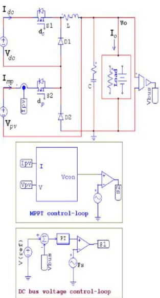
II. DESIGNING OF TWO INPUT INTEGRATED BUCK-BOOST CONVERTER
The proposed TIBBC, shown in Fig. 1, is essentially a parallel combination of buck and buck-boost converter. It is possible to connect the two converters in parallel at the load terminals, but to reduce the number of energy storage elements [5], the
a manner so that only one inductor “L” is sufficient for processing the power in the both the converters. Single inductor based integrated topologies are having several advantages, of which the most important one are: (i) results in simple second order system and easy to understand it’s dynamical behavior, (ii) reduced number of magnetic cores and thus size of the converter, and (iii) single filter capacitor is sufficient to realize the desired load voltage ripple. In view of reduction in its order understanding the dynamical issues and then addressing controller design issues are now becomes easier. The circuit can actually operate either in continuous or discontinuous inductor current mode. But, it’s operation in discontinuous mode of operation will not provide benefits for the power conversion, and also on the account of its location in the circuit maintains the current flows for almost all loading conditions. In view of this the circuit operation is discussed only for continuous inductor
current mode (CICM). In CICM the TIBBC goes
through three topological stages, in each switching period, and their dynamics can be described by a set of state-space equations given by:
for mode-1,mode-2 and 3, respectively. Applying the state-space averaging analysis [8] and upon simplification results in the average model where A= (A1d1+A2d2+A3d3), B=
(B1d1+B2d2+B3d3) given below
Here the circuit operation depends on the type of controlling signals used for the switching devices S1 and S2. In any case
the switches must be synchronized. Each of these schemes has their own advantages and limitations and detailed discussion on the suitability and application requirements is beyond the scope of this paper.
Fig. 1.Control of Multi-input Buck & Buck-Boost Converter.
It is possible to connect the two converters in parallel at the load terminals, but to reduce the number of energy storage elements [5], the switching devices of the two converters are arranged in such a manner so that only one inductor “L” is sufficient for processing the power in the both the converters. Single inductor based integrated topologies are having several advantages, of which the most important one are:
2. Reduced number of magnetic cores and thus size of the converter, and
3. Single filter capacitor is sufficient to realize the desired load voltage ripple.
In view of reduction in its order understanding the dynamical issues and then addressing controller design issues are now becomes easier. The circuit can actually operate either in continuous or discontinuous inductor current mode. But, its operation in discontinuous mode of operation will not provide benefits for the power conversion, and also on the account of its location in the circuit maintains the current flows for almost all loading conditions. In view of this the circuit operation is discussed only for continuous inductor current mode (CICM).
In this TIBBC the diodes will be the integral part of both the converters, buck and buck-boost topologies, while the switching devices are still part of the individual converters. Load and it’s filtering capacitor are common to both the converters. Buck converter is formed by: S1, D1, D2, L, R; while Buck-boost converter is formed by: S2, D1, D2, L, R. The steady-state load voltage can easily be established, either by employing volt-sec balance or through state-space model,
For a given solar insolation the maximum power generation capability of PV is fixed and depending on the dc bus voltage (V0) the buck boost converter duty cycle (dp) will be adjusted,
by the MPPT control-loop, and supplies load current Io1. If ‘ᶯ1’ is the MPPT converter efficiency, the amount of load
current supplied by PV array can be easily obtained by applying the principle of power balance is,
where Vmp, Impare the PV array maximum power point
array voltage and current, respectively. If the load demand is “Io=(Io1+Io2)” then this load is distributed among the two power sources, PV and battery. The PV supplies “I o1”, while the rest will be drawn from the dc source. Amount of load current supplied by the DC source is
III. CONTROL STRATEGY FOR BUS VOLTAGE REGULATION
Several different types of control strategies are reported in literature and they are broadly classified into: (i) single-loop voltage-mode, (ii) single-loop current-mode, (iii) two-loop current mode control, and (iv) multi-loop schemes. Among these the single-loop control strategies are simple to implement, but at the expense of higher dynamic response time. Although the two-loop current-mode control schemes are popular in the power supply applications, but their compensator design becomes complex in the PV supplied hybrid systems.
In this paper for the TIBBC two interdependent control strategies, one for bus voltage regulation and the other for MPPT, are proposed. This structure is capable of maintaining the load voltage regulation while extracting the maximum available power from the PV renewable source. The control schemes can be interchangeable from one to other depending on the source power supply capacity. However, use of MPPT loop for the buck converter imposes the constraints on the load for extracting maximum power.
In view of this difficulty it is always recommended to use MPPT loop with the buck-boost topology, as it is having capability of extracting maximum power for most of the loading conditions.
To demonstrate the control principle an MPPT loop for the buck- boost converter and voltage control-loop for the buck converter, as shown in Fig. 1, are used in this paper. Properly tuned proportional plus integral (PI) controller is capable of achieving reasonable dynamic response times both for line and load changes. For PV source the MPPT loop is designed using the well established perturb and observation algorithm (POA) [7].
The PI controller is designed here for the stand-alone buck converter to ensure dc bus voltage regulation assuming it is supplying the full rated load demand. Block diagram for the control loop design is shown in Fig. 2 where-in Gvd(s): control-to-output transfer function, Gc(s): Compensator, Fm: PWM generator transfer function, ‘K’ is the load voltage sensing gain, and loop gain TL(s)=KFmGc(s)Gvd(s).
The compensator is designed in the frequency domain approach and uses pole zero placement technique. Fine tuning of the compensator is performed to ensure the optimum stability margins, i.e. gain margin> 6 dB, 0<phase margin<750.
Fig. 2. Control-loop design block diagram for bus voltage regulation.
Parameters
Value
Inductor ( L )
100 µH
Capacitor ( C )
200 µF
Capacitive resistance ( r
c)
0.047 Ω
Inductive resistance ( r
l)
0.047 Ω
Load resistance ( R )
2 Ω
Switching Frequency(
F
s )
5 kHz
Table 1: Simulation parameters
IV. SIMULATION AND RESULTS
The performance of Multi in-put integrated buck and buck-boost converter steady state performance is analyzed and dynamic behavior is studied, for the three steady state cases are analyzed, they are:
Case-1: Load Sharing at Constant Rated Solar Insolation, Case-2: Load Redistribution for Variable Solar Insolation Case-3: Change in Load Demand
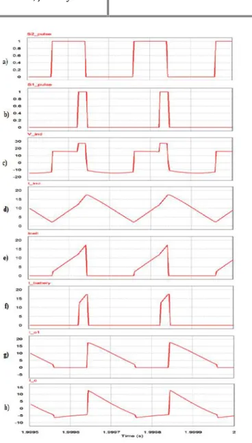
Figure 3: Typical voltage and current waveforms for key components of the TIBBC
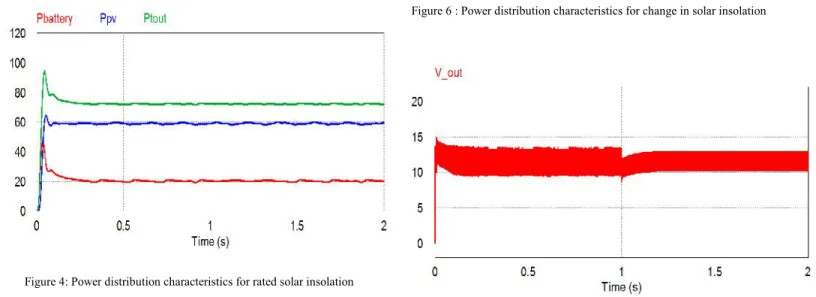
Figure 4: Power distribution characteristics for rated solar insolation
Figure 5: Out-put voltage characteristics for rated solar insolation
Case-2: Load Redistribution for Variable Solar Insolation When solar insolation decreases, to 50% of rated insolation, then the power generation capacity of the PV array becomes low, 30 W. From this instant onwards the dc source has to supply 48 W to meet the fixed load demand of 72 W and the corresponding results are shown in Fig.6, Fig.7 & Fig.8
Figure 6 : Power distribution characteristics for change in solar insolation
Figure 7: Out-put voltage characteristics for change in solar insolation
Figure 8: Change in solar isolation (from 1000 to 500 Wp /m2)
Case-3: Change in Load Demand
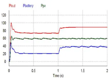
Fig.9 Power distribution characteristics against load changes (Po: 72 to 87 w )
Fig 10: Out-put voltage characteristics against load changes (Po: 72 to 87 w )
V.CONCLUSIONS
Two input buck-boost integrated converter suitable for the PV applications was proposed. Single-loop voltage-mode control strategy for buck converter, to ensure dc bus voltage regulation, while maximum power point tracking algorithms for the buck-boost converter were implemented. The proposed control scheme effectiveness was tested for different cases and then the following conclusions were drawn from this study:
1. in almost all cases the total load demand is met by the two sources,
2. at all solar insolations the buck-boost converter extracted the maximum power
3. dc bus voltage regulation was achieved irrespective of the power supplied by the PV source,
4. Load changes are reflecting on the fixed dc source, 5. Connected through buck converter, while extracting
the maximum available power from the PV source, which ensures maxim utilization of the renewable source. The results are in agreement with the theoretical predictions.
6. Jury stability analysis is applied to Multi-input integrated Buck and Buck-Boost converter and found system is completely stable.
REFERENCES
1.Jian Liu, Zhiming Chen, Zhong Du, “A new design of power supplies for pocket computer system”, IEEE Trans. on Ind. Electronics, 1998, Vol. 45(2), pp. 228-234.
2.Francis D. Rodriguez, William G. Imes, “Analysis and modeling of a two-input dc/dc converter with two controlled variables and four switched networks,” Intersociety Energy Conversion Engineering Conference (IECEC), 1996, pp. 322-327.
3.Mario Marchesoni, Camillo Vacca, “New dc-dc converter for energy storage system interfacing in fuel-cell hybrid vehicles, IEEE Trans on Power Electronics, 2007, Vol. 22(1), pp. 301-308. 4.Hirofumi Matsuo, Wenzhong Lin, Fujio Kurokawa,
Tetsuro Shigemizu, Nobuya Watanabe, “Characteristics of the multiple-input dc-dc converter,” IEEE Trans on Ind. Electronics, 2004, Vol. 51(3), pp. 625-631.
5.Yaow Ming Chen, Yuan Chuan Liu, Sheng Hsien Lin, “Double-input PWM dc/dc converter for high/low voltage sources,” IEEE Trans on Ind. Electronics, 2006, Vol. 53(5), pp. 1538-1545. 6.K. P. Yalamanchili, M. Ferdowsi, Keith Corzine,
“New Double input dc-dc converters for automotive applications", IEEE Applied Power Electronics Conference (APEC), 2006, CD-ROM proceddings.
7.Veerachary. M, Senjyu. T, Uezato. K, `Maximum power point tracking control of IDB converter supplied PV system,'' IEE Proc. Electr. Power Appl., 2001, vol. 148(6), pp. 494-502.
9.R.D.Middlebrook, Cuk.S, “A general unified approach to modeling switching converter power stage”, IEEE Power electronics specialists conference, 1976, pp. 13-34.
10. Katsuhiko Ogata “Discrete-Time Control System” Prentice-Hall, Inc Publishers.
11. Chetan singh Solanki “Solar photovoltaic’s fundamentals, technologies and applications” phi Learning (P) Ltd, 2011.
12. “PSIM User’s Guide” Version 9.0, Release 3, May 2010.
AUTHOR’S PROFILE
G.D.V.PRASANTH Pursuing M.Tech in BVC Engineering Collage, Odalarevu .His specialization is Power Electronics. He graduated in Electrical and Electronics Engineering from Regency Institute of Tech, Pondicherry University. His research interest includes Power Electronics converters and Drives. ([email protected])