Contents
1. The Electron and its Properties ... 2
1.1. History ... 2
1.2. Wave properties ... 2
1.3. Characteristics of the electron wave 3
2. Electron-Matter Interactions ... 4
2.1. Introduction ... 4
2.2. Basic Definitions ... 4
3. Elastic Interactions ... 5
3.1. Incoherent Scattering of Electrons at an Atom ... 5
3.1.1. Basics ... 5
3.1.2. Interaction cross-section and mean free path ... 5
3.1.3. Differential cross section ... 7
3.1.4. Interaction volume ... 7
3.2. Contrast Generation in the Electron Microscope ... 8
3.2.1. Basics ... 8
3.2.2. Bright field imaging ... 9
3.2.3. Applications of high angle scattering ... 10
3.3. Coherent Scattering of Electrons at a Crystal ... 12
3.3.1. Basics ... 12
3.3.2. Bragg equation ... 13
3.3.3. Electron diffraction ... 14
3.3.4. Bragg contrast ... 15
4. Inelastic Interactions ... 17
4.1. Introduction ... 17
4.2. Inner-Shell Ionization ... 17
4.2.1. Characteristic X-rays ... 17
4.2.2. Auger electrons ... 19
4.2. Braking radiation ... 20
4.3. Secondary electrons ... 20
4.4. Phonons ... 20
4.5. Plasmons ... 20
4.6. Cathodoluminescence ... 21
4.7. Electron energy loss spectroscopy (EELS) ... 21
4.7. Beam damage ... 23
4.8. Origin of signals ... 23
Properties of Electrons, their Interactions with Matter
and Applications in Electron Microscopy
By Frank KrumeichLaboratory of Inorganic Chemistry, ETH Zurich, Vladimir-Prelog-Weg 1, 8093 Zurich, Switzerland
1. The Electron and its
Properties
1.1. History
The electron e is an elementary particle that carries a negative charge. Although the phenomenon of electricity was already known in ancient Greece1 and numberless investigations had been made in the intermediate centuries, the electron was finally discovered by J. J. Thompson in 1897 (Nobel Prize 1906). While studying so-called cathode rays, which in fact are electron beams, he discovered that these rays are negatively charged particles, which he called “corpuscles”. Moreover, he found out that they are constituents of the atom and over 1000 times smaller than a hydrogen atom. In fact, the mass of the electron is approximately 1/1836 of that of a proton.
1.2. Wave properties
In 1924, the wave-particle dualism was postulated by de Broglie (Nobel Prize 1929). All moving matter has wave properties (Figure 1), with the wavelength being related to the momentum p by
= h / p = h / mv
(h : Planck constant; m : mass; v : velocity) This equation is of fundamental importance for electron microscopy because this means that accelerated electrons act not only as
1 The electron is named after the Greek word for
amber.
particles but as waves too. Consequently, the wave length of moving electrons can be calculated from this equation taking their energy E into consideration. An electron accelerated in an electric field V gains an energy E = eV which further corresponds to a kinetic energy Ekin = mv2/2. Thus:
E = eV = m0v2 / 2.
From this, the velocity v of the electron can be derived:
(V : acceleration voltage; e : electron charge = -1.602 176 487 × 10-19 C; m0 : rest mass of
the electron = 9.109 x 10⁻³¹ kg).
It follows for the momentum p of the electron:
0 0
= m v = 2m eV
p
Now, the wavelength can be calculated from the de Broglie equation according to
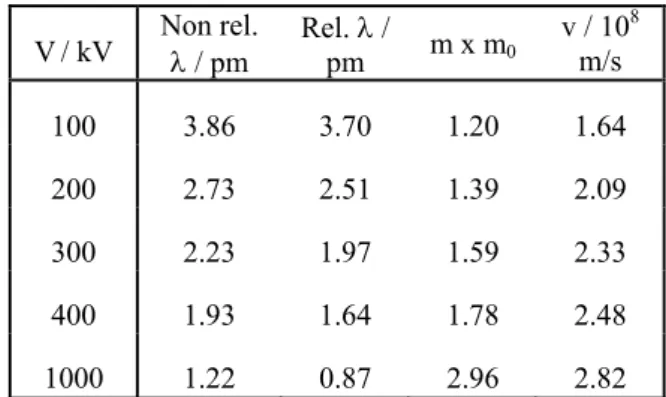
The values calculated for acceleration potentials commonly used in TEM are listed in Table 1. It is important to note that these electrons move rather fast, and their speed approaches light velocity. As a result, a term considering relativistic effects must be added:
V/ kV Non rel. / pm Rel. pm / m x m0 v / 10 8
m/s 100 3.86 3.70 1.20 1.64 200 2.73 2.51 1.39 2.09 300 2.23 1.97 1.59 2.33 400 1.93 1.64 1.78 2.48 1000 1.22 0.87 2.96 2.82
Table 1: Properties of electrons depending on the acceleration voltage.
Figure 1: Basic definitions of a wave.
0 2eV v =
m
0
= h 2m eV
2
0 0
= h 2m eV (1 + eV / 2m c )
(c : light velocity in vacuum = 2.998 x 10⁸ m/s).
Of course, the difference between the values calculated with and without considering relativistic effects increases with increasing acceleration potential and thus increasing electron speed. This is demonstrated in Table 1 by giving the hypothetical non-relativistic and the relativistic wavelength . While the difference exceeds 30% for 1000 kV electrons, it still is ca. 5% at 100 kV. This effect is also recognizable by regarding the relativistic increase of the actual electron mass: at 100 kV, it is already 1.2 x of the rest mass m0; at 1000 kV, it is almost 3 x m0. The
velocity of the electron increases also drastically with the acceleration voltage and has reached ca. 90% of light velocity c at 1000 kV. Please note that the velocity calculated without considering relativistic effects would exceed c, the maximum velocity that is possible according to Einstein’s special relativity theory, already for 300 kV electrons. It thus is evident that relativistic effects cannot be neglected for electrons with an energy E ≥ 100 kV.
1.3. Characteristics of the electron
wave
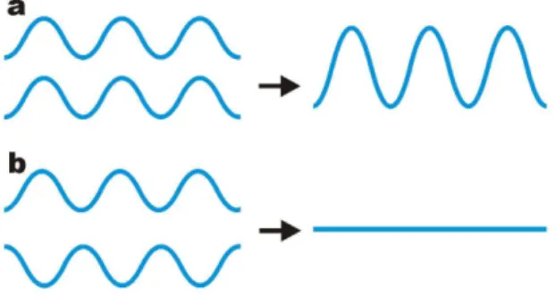
Waves in beams of any kind can be either coherent or incoherent. Waves that have the same wavelength and are in phase with each
other are designated as coherent. In phase with each other means that the wave maxima appear at the same site (Figure 2). The analogue in light optics is a Laser beam. On contrast, beams comprising waves that have different wavelengths like sun rays or are not in phase are called incoherent (Figure 2). Electrons accelerated to a selected energy have the same wavelength. Depending on the electron gun, the energy spread and as a result the wave length as well varies. Furthermore, the electron waves are only nearly in phase with each other in a thermoionic electron gun while the coherency is much higher if a field emitter is the electron source. The generation of a highly monochromatic and coherent electron beam is an important challenge in the design of modern electron microscopes. However, it is a good and valid approximation to regard the electron beam as a bundle of coherent waves before hitting a specimen. After interacting with a specimen, electron waves can form either incoherent or coherent beams.
Waves do interact with each other. By linear superposition, the amplitudes of the two waves are added up to form a new one. The interference of two waves with the same wavelength can result in two extreme cases (Figure 3):
(i) Constructive interference: If the waves are completely in phase with each other, meaning that the maxima (and minima) are at the same position and have the same
Figure 2: Scheme showing coherent (top) and incoherent waves (bottom).
Figure 3: Interference of two waves with the same wavelength and amplitude. (a) Constructive interference with the waves being in phase. (b) Destructive interference with the waves being exactly out of phase.
amplitude, then the amplitude of the resulting wave is twice that of the original ones.
(ii) Destructive interference: If two waves with the same amplitude are exactly out of phase, meaning that the maximum of one wave is at the position of the minimum of the other, they are extinguished.
2. Electron-Matter Interactions
2.1. Introduction
Electron microscopy, as it is understood today, is not just a single technique but a diversity of different ones that offer unique possibilities to gain insights into structure, topology, morphology, and composition of a material. Various imaging and spectroscopic methods represent indispensable tools for the characterization of all kinds of specimens on an increasingly smaller size scale with the ultimate limit of a single atom. Because the observable specimens include inorganic and organic materials, micro and nano structures, minerals as well as biological objects, the impact of electron microscopy on all natural sciences can hardly be overestimated.
The wealth of very different information that is obtainable by various methods is caused by the multitude of signals that arise when an electron interacts with a specimen. Gaining a basic understanding of these interactions is an essential prerequisite before a comprehensive introduction into the electron microscopy methods can follow.
A certain interaction of the incident electron with the sample is obviously necessary since without the generation of a signal no sample properties are measurable. The different types of electron scattering are of course the basis of most electron microscopy methods and will be introduced in the following.
2.2. Basic Definitions
When an electron hits onto a material, different interactions can occur, as summarized in Figure 4. For a systemization, the interactions can be classified into two different types, namely elastic and inelastic interactions.
(i) Elastic Interactions
In this case, no energy is transferred from the electron to the sample. As a result, the electron leaving the sample still has its original energy E0:
Eel = E0
Of course, no energy is transferred if the electron passes the sample without any interaction at all. Such electrons contribute to the direct beam which contains the electrons that passes the sample in direction of the incident beam (Figure 4).
Furthermore, elastic scattering happens if the electron is deflected from its path by Coulomb
Figure 4: Scheme of electron-matter interactions arising from the impact of an electron beam onto a specimen. A signal below the specimen is only observable if the thickness is small enough to allow some electrons to pass through.
interaction with the positive potential inside the electron cloud. By this, the primary electron loses no energy or – to be accurate – only a negligible amount of energy. These signals are mainly exploited in TEM and electron diffraction methods.
(ii) Inelastic Interactions
If energy is transferred from the incident electrons to the sample, then the electron energy of the electron after interaction with the sample is consequently reduced:
Eel < E0
The energy transferred to the specimen can cause different signals such as X-rays, Auger or secondary electrons, plasmons, phonons, UV quanta or cathodoluminescence. Signals caused by inelastic electron-matter interactions are predominantly utilized in the methods of analytical electron microscopy. The generation and use of all elastic and inelastic interactions will be discussed in some detail in the following chapters.
3. Elastic Interactions
3.1. Incoherent Scattering of
Electrons at an Atom
3.1.1. Basics
For the rudimentary description of the elastic scattering of a single electron by an atom, it is sufficient to regard it as a negatively charged particle and neglect its wave properties.
An electron penetrating into the electron cloud of an atom is attracted by the positive potential of the nucleus (electrostatic or Coulombic interaction), and its path is deflected towards the core as a result (Figure 5). The Coulombic force F is defined as:
F = Q1Q2 / 4πεo r2
(r : distance between the charges Q1 and Q2; εo : dielectric constant).
The closer the electron comes to the nucleus, i.e. the smaller r, the larger is F and consequently the scattering angle. In rare cases, even complete backscattering can occur, generating so-called back-scattered electrons (BSE). These electrostatic electron-matter interactions can be treated as elastic, which means that no energy is transferred from the scattered electron to the atom. In general, the Coulombic interaction is strong, e.g. compared to the weak one of X-rays with materials.
Because of its dependence on the charge, the force F with which an atom attracts an electron is stronger for atoms containing more positives charges, i.e. more protons. Thus, the Coulomb force increases with increasing atomic number Z of the respective element.
3.1.2. Interaction cross-section and mean free path
If an electron passes through a specimen, it may be scattered not at all, once (single
Figure 5: Scattering of an electron inside the electron cloud of an atom.
scattering), several times (plural scattering), or many times (multiple scattering). Although electron scattering occurs most likely in forward direction, there is even a small chance for backscattering (Figure 5).
The chance that an electron is scattered can be described either by the probability of a scattering event, as determined by the interaction cross-section , or by the average distance an electron travels between two interactions, the mean free path .
The concept of the interaction cross-section is based on the simple model of an effective area. If an electron passes within this area, an interaction will certainly occur. If the cross-section of an atom is divided by the actual area, then a probability for an interaction event is obtained. Consequently, the likelihood for a definite interaction increases with increasing cross-section.
The probability that a certain electron interacts with an atom in any possible way depends on the interaction cross section . Each scattering event might occur as elastic or as inelastic interaction. Consequently the total interaction cross section is the sum of all
elastic and inelastic terms: elastinelast.
It should be mentioned here that each type of possible interaction of electrons with a material has a certain cross section that moreover depends on the electron beam energy. For every interaction, the cross-section can be defined depending on the effective radius r:
= r2.
For the case of elastic scattering, this radius relast is
relast = Z e / V
(Z : atomic number; e : elementary charge; V : electron potential; : scattering angle).
This equation is important for understanding some fundamentals about image formation in several electron microscopy techniques. Since
the cross-section and thus the likelihood of scattering events as well increases for larger radii, scattering is stronger for heavier atoms (with high) Z than for light elements. Moreover, it indicates that electrons scatter less at high voltage V and that scattering into high angles is rather unlikely.
By considering that a sample contains a number of N atoms in a unit volume, a total scattering interaction cross section QTis given
as
QT = N = N0 T / A
(N0 : Avogadro number; A : atomic mass of
the atom of density ).
Introducing the sample thickness t results in QT t = N0 T (t) / A.
This gives the likelihood of a scattering event. The term t is designated as mass-thickness. Doubling leads to the same Q as doubling t. In spite of being rather coarse approximations, these expressions for the interaction cross-section describe basic properties of the interaction between electrons and matter reasonably well.
Another important possibility to describe interactions is the mean free path , which unfortunately has usually the same symbol as the wavelength. Thus, we call it mfp here for
clarity. For a scattering process, this is the average distance that is traveled by an electron between two scattering events. This means, for instance, that an electron in average interacts two times within the distance of 2mfp. The mean free path is
related to the scattering cross section by: mfp = 1 / Q.
For scattering events in the TEM, typical mean free paths are in the range of some tens of nm.
For the probability p of scattering in a specimen of thickness t follows then:
3.1.3. Differential cross section
The angular distribution of electrons scattered by an atom is described by the differential cross section d/d. Electrons are scattered by an angle and collected within a solid angle (Figure 6). If the scattering angle increases, the cross-section decreases. Scattering into high angles is rather unlikely. The differential cross-section is important since it is often the measured quantity.
3.1.4. Interaction volume
To get an idea about how the scattering takes part in a certain solid, Monte Carlo simulations can be performed.2 As the name already indicates, this is a statistical method using random numbers for calculating the paths of electrons. However, the probability of
2 An on-line version can be found on the page:
www.matter.org.uk/tem.
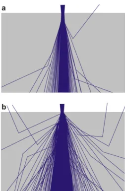
scattering is taken into account by the programs as well as important parameters like voltage, atomic number, thickness, and the density of the material. Although such calculations are rather rough estimates of the real physical processes, the results describe the interaction and, in particular, the shape and size of the interaction volume reasonably well. The following figures show schemes of such scattering processes.
As mentioned before, most electrons are scattered not at all or in rather small angles (forward scattering). This is evident if the scattering processes in thin foils (as in TEM samples) are regarded (Figure 7). Scattering in high angles or even backwards is unlikely in all materials but the likelihood for them increases with increasing atomic number Z. Furthermore, the broadening of the beam increases with Z. As a general effect, the intensity of the direct beam is weakened by the deflection of electrons out of the forward direction. Since this amount of deflected electron and thus the weakening of the beam intensity depend strongly on Z, contrast between different materials arises.
Figure 6: Annular distribution of electron scattering after passing through a thin sample. The scattering semiangle (and incremental changes d, respectively) and the solid angle of their collection (and incremental changes d, respectively) are used to describe this process quantitatively.
Figure 7: Interaction of an electron beam with a (a) low Z and (b) high Z material. Most electron are scattered forward. Beam broadening and the likelihood of scattering event into high angles or backwards increase with higher Z.
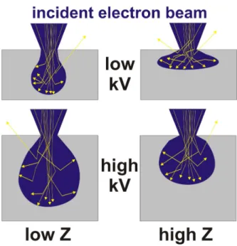
Analogous results are obtained if compact samples are considered (Figure 8). Here, most electrons of the incoming electron beam are finally absorbed in the specimen resulting in an interaction volume that has a pear-like shape. On their path through the sample, electrons interact inelastically losing a part of their energy. Although this probability of such events is rather small, a lot of them appear if the sample is thick, i.e. the path of the electron through the sample long. The smaller the energy of the electron is, the higher the likelihood of its absorption in the sample becomes. However, some of the incoming electrons are even back-scattered. The dependence of the shape of the interaction volume on the material and the voltage is schematically demonstrated in Figure 8. The size of the interaction volume and the penetration depth of the electrons increase with increasing electron energy (voltage) and decrease with atomic number of the material (high scattering potential).
3.2. Contrast Generation in the
Electron Microscope
3.2.1. Basics
The simple model of elastic scattering by Coulomb interaction of electrons with the atoms in a material is sufficient to explain basic contrast mechanisms in electron microscopy. The likelihood that an electron is deviated from its direct path by an interaction with an atom increases with the number of charges that the atom carries. Therefore, heavier elements represent more powerful scattering centers than light element. Due to this increase of the Coulomb force with increasing atomic number, the contrast of areas in which heavy atoms are localized will appear darker than of such comprising light atoms. This effect is the mass contrast and schematically illustrated in Figure 9.
Furthermore, the number of actually occurring scattering events depends on the numbers of atoms that are lying in the path of the electron. As the result, there are more electrons scattered in thick samples than in thin ones. Therefore, thick areas appear darker than thin areas of the same material. This effect leads to thickness contrast.
Together, these two effects are called mass-thickness contrast (Figure 9). This contrast can be understood quite intuitively since it is somehow related to the contrast observed in
Figure 8: Interaction volumes of the incident electron beam (blue) in compact samples (grey) depending on electron energy and atomic number Z. The trajectories of some electrons are marked by yellow lines.
Figure 9: Schematic representation of contrast generation depending of the mass and the thickness of a certain area.
optical microscopy. However, instead of absorption of light, it of course is the local scattering power that determines the contrast of TEM images.
In particular, this concept of mass-thickness contrast is important to understand bright field TEM and STEM images.
3.2.2. Bright field imaging
In the bright field (BF) modes of the TEM and the STEM, only the direct beam is allowed to contribute to image formation. This is experimentally achieved on two different ways. In the TEM, a small objective aperture is inserted into the back focal plane of the objective lens in such a way that exclusively the direct beam is allowed to pass its central hole and to build up the image (Figure 10). Scattered electrons are efficiently blocked by the aperture.
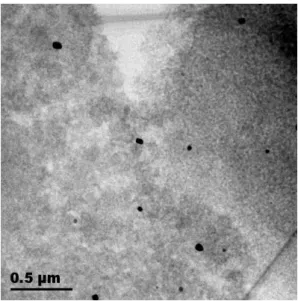
The direct beam is utilized for image formation in an analogous way in a STEM: here, a bright field detector is placed in the path of the direct beam. Resultantly, scattered electrons are not detected by BF-STEM. It is essentially the weakening of the direct beam’s intensity that is detected by both types of BF imaging. A main component of this weakening is the mass-thickness contrast. As an example for pure thickness contrast, the BF-TEM image of a silica particle supported on a carbon foil is reproduced in Figure 11. Thin areas of the particle appear brighter than thick ones. This effect can also be recognized at the supporting C foil: in thin areas close to the hole in the foil, the C foil is thin and therefore its contrast is light grey whereas it is darker in the middle of the foil (area marked by “C” in Figure 11).
The effect of large differences in mass is visible in a BF-TEM image of gold particles on titania (Figure 12). The particles with a size of several 10 nm appear with black contrast since Au is by far the heaviest element in this system and therefore scatters many electrons. Furthermore, the Au particles
are crystalline, and as a result Bragg contrast contributes to the dark contrast as well (see below). The titania support appears with an almost uniform grayness. However, the thickness of the area in the upper right corner of the image is greater as indicated by the darker contrast there (thickness contrast).
Figure 10: Contrast generation in BF-TEM mode. Scattered beams are caught by the objective aperture and only the direct beam passes through the central hole and contributes to the final image.
thin
thick
C
Figure 11: BF-TEM image of a SiO2 particle on a holey
3.2.3. Applications of high angle scattering
As discussed above, the Coulomb interaction of the electrons with the positive potential of an atom core is strong. This can lead to scattering into high angles (designated as Rutherford scattering) or even to back-scattering (cf. Figure 5). The fact that the probability of such scattering events rises for heavier atoms, i.e. atoms with a high number of protons and consequently a high atomic number Z, offers the possibility for obtaining chemical contrast. This means that areas or particles containing high Z elements scatter stronger and thus appear bright in images recorded with electrons scattered into high angles or even backwards.
This effect is employed in high-angle annular dark field (HAADF) STEM (also called Z-contrast imaging) and in SEM using back-scattered electrons (BSE). By the HAADF-STEM method, small clusters (or even single atoms) of heavy atoms (e.g. in catalysts) can be recognized in a matrix of light atoms since contrast is high (approximately proportional to Z2).
This is in particular a valuable method in heterogeneous catalysis research where the determination of the size of metal particles and the size distribution is an important
question. If the metal has a higher Z than the elements of the support, which is frequently the case, Z contrast imaging is very suitable. For example, a few nm large gold particles can be easily recognized by their bright contrast on a titania support (Figure 13). Besides secondary electrons (SE), back-scattered electrons (BSE) can be utilized for image formation in the scanning electron microscope (SEM). While SE images show mainly the topology of the sample surface, particles or areas with high Z elements appear with bright contrast in BSE images (material contrast). The example of platinum on aluminum oxide (Figure 14) demonstrates this: small Pt particles appear with bright contrast in the BSE image but are not recognizable in the SE image.
Though the contrast generation in HAADF-STEM (Z contrast) and BSE-SEM images is basically due to the same physical reasons, the resolution of both methods is strikingly different: Z contrast has been proven able to detect single atoms whereas BSE-SEM has only a resolution of a few nm for the best microscopes and detectors.
Figure 12: BF-TEM image of Au particles (black patches) on a TiO2 support.
50 nm 50 nm
Figure 13: HAADF-STEM image of Au particles (bright) on TiO2.
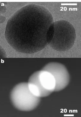
As in TEM, thickness effects contribute to the image contrast in HAADF-STEM. An example is shown in Figure 15. Ball-like palladium particles are partly overlapping each over. At the intersections, the thickness – and resultantly the scattering power as well – of two particles sums up and is thus increased compared to that of the a single ball. In the TEM image, this leads to a darker contrast whereas in the HAADF-STEM image the contrast in the intersections becomes brighter than in the single balls.
Figure 14: SEM images of Pt on Al2O3 recorded with
secondary (top) and back-scattered electrons (bottom).
Figure 15: (a) TEM and (b) HAADF-STEM image of Pd balls on silica. The overlap regions are relatively dark in (b) and bright in (b), respectively, due to the increased thickness there.
3.3. Coherent Scattering of Electrons
at a Crystal
3.3.1. Basics
Solely incoherent scattering of the incident, nearly coherent electrons takes part if the scattering centers are arranged in an irregular way, especially in amorphous compounds. Although the scattering happens pre-dominantly in forward direction, the scattered waves have arbitrary phases in respect of each other. An enhancement of the wave intensity in certain directions because of constructive interference can thus not happen.
On the other hand, if a crystalline specimen3 is transmitted by electrons with a certain wavelength 0, then coherent scattering takes
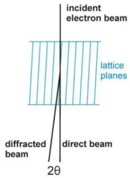
place. Naturally, all atoms in such a regular arrangement act as scattering centers that deflect the incoming electron from its direct path. This occurs in accordance with the electrostatic interaction of the nucleus with the negatively charged electron discussed above. Since the spacing between the scattering centers is regular now, constructive interference of the scattered electrons in certain directions happens and thereby diffracted beams are generated (Figure 16). This phenomenon is called Bragg diffraction. To explain diffraction, regarding the electron as a particle is not sufficient and consequently its wave properties must be taken into account here as well.
In analogy to the Huygens principle describing the diffraction of light, all atoms can then be regarded as the origins of a secondary spherical electron wavelet that still has the original wavelength 0. Obviously,
these wavelets spread out in all directions of space and in principle do interfere with each other everywhere. From a practical point of
3 A crystal is characterized by an array of atoms that is
periodic in three dimensions. Its smallest repeat unit is the unit cell with specific lattice parameters, atomic positions and symmetry.
view, this interference is most intense in forward direction. The generation of diffracted beams is schematically demonstrated in Figure 17a,b. For simplicity, only a row of atoms is regarded as a model for regularly arranged scattering centers in a crystal lattice, and the three-dimensional secondary wavelets are represented by two-dimensional circles
It is important to note that the maxima of the secondary wavelets are in phase with each other in well-defined direction. The most obvious case is the direction of the incoming parallel electron wave that corresponds to the direct (not diffracted) beam after passing the specimen. The maxima of the wavelets appear in the same line there and form a wave front by constructive interference (Figure 17a). However, such lines of maxima forming planes of constructive interference occur in other directions as well (Figure 17b).
In the first case, the first maximum of the wavelet of the first atom forms a wave front with the second maximum of the second atom’s wavelet, with the third atom’s third maximum and so forth. This constructive interference leads to a diffracted electron
Figure 16: Diffraction of an electron beam by a crystal. The crystal is schematically represented by a set of parallel equidistant lattice planes.
beam, designated as 1st order beam. This beam has the smallest diffraction angle observed here (Figure 17b). The 2nd order beam is basically formed by the interference of the first maximum of the wavelet of the first atom with the third maximum of the second atom’s wavelet, the fifth maximum of the third atom and so forth. Together, all diffracted beams give rise to a diffraction pattern.
3.3.2. Bragg equation
The simple model used in Figure 17a,b for explaining the generation of diffracted beams can also provide ideas how the diffraction angle depends on the interatomic distance and the wavelength of the electrons.
A smaller interatomic distance gives rise to a higher density of the secondary wavelets and a smaller distance between them (Figure 17c). The diffraction angle, as depicted here for the first order beam, is resultantly smaller as for a larger interatomic distance (compare Figure 17 b and c).
If the wavelength of the incident electron beam is changed, this is also the case for that of the secondary wavelength. Consequently, the diffraction angle changes as well. An increase of the wavelength results in an increase of the diffraction angle (compare Figure 17 b and d).
To find a quantitative expression for the relation between diffraction angle, electron wavelength and interatomic distance, we regard the diffraction of an incoming electron
Figure 17: Model for the diffraction of an electron wave at a crystal lattice. The interaction of the incident plane electron wave with the atoms leads to equidistant secondary wavelets that constructively interfere with each other in (a) forward and (b) other directions. The angle between the direct and the diffracted beam (diffraction angle) increases (c) with decreasing interatomic distance and (d) with increasing wavelength. All waves are represented schematically by their maxima.
wave at a set of equidistant lattice planes. In this simplified model, the diffraction is treated as a reflection of the electron wave at the lattice planes. This description leads to a general equation that is valid not only for diffraction of electrons but for that of X-rays and neutrons as well although it is far from physical reality.4
The conditions for constructive interference for two electron waves diffracted at two parallel lattice planes packed with atoms are depicted in Figure 18. The two incident electron waves are in phase with each other (left side). After reflection at the lattice planes, the two waves have to be in phase again for constructive interference. For this, the distance that the wave with the longer path follows needs to be an integer multiple of the electron wavelength. This path depends on the incident angle , the distance between the lattice planes d and the electron wavelength el. The path length is twice d•sin. Since this
value must be a multiple of el, it follows:
2d sin = n.
This is the Bragg equation for diffraction. From this equation, an idea about the size of the scattering angles is obtainable. For 300 kV, the wavelength is = 0.00197 nm. For a d-value of 0.2 nm, one calculates an angle of 0.28°. As a rule, diffraction angles in electron diffraction are quite small and typically in the range 0° < < 1°. This is a
4 Remember: As any deflection of electrons, electron
diffraction is basically caused by Coulomb interaction of electrons with the positive potential inside the electron cloud of an atom.
consequence of the small wavelength.5 Furthermore, the reflecting lattice planes are almost parallel to the direct beam. Thus, the incident electron beam represents approximately the zone axis of the reflecting lattice planes (Figure 19).
From the Bragg equation, it can directly be understood that the increase of the wavelength and the decrease of the d value lead to an increase of the scattering angle (cf. Figure 17).
3.3.3. Electron diffraction
Depending on the size of the investigated crystallites, different types of electron diffraction patterns are observed. If exclusively a single crystal contributes to the diffraction pattern, then reflections appear on well-defined sites of reciprocal space that are characteristic for the crystal structure and its lattice parameters (Figure 19). Each set of parallel lattice planes that occur in the investigated crystal and in the zone axis
5 Note that the scattering angles in X-ray reflection are
in the range 0° > > 180°, due to the larger wave lengths (e.g. ca. 0.14 nm for CuK radiation).
Figure 18: Diffraction at a set of two parallel lattice planes, demonstrating the conditions for constructive interference.
Figure 19: Scheme showing the generation of two diffraction spots by each set of lattice planes, which are represented by a single one here.
selected give rise to two spots with a distance that is in reciprocal relation to that in real space. Thus large d-values cause a set of points with a narrow distance in the diffraction pattern, whereas small d-values cause large distances. This is a principle of the
reciprocal space.
If more than one crystal of a phase contributes to the diffraction pattern, as it is the case for polycrystalline samples, then the diffraction patterns of all crystals are superimposed. Since the d-values and thus the distances in reciprocal space are the same, the spots are then located on rings (Figure 20). Such ring patterns are characteristic for polycrystalline samples.
An example for a diffraction pattern of a single crystal is shown in Figure 21a. It represents the electron diffraction pattern of a tantalum telluride with a complex structure. The spots are located on a square array that is typical for structures with a tetragonal unit cell observed along [001].
The electron diffraction pattern of polycrystalline platinum shows diffraction rings (Figure 21b). Some larger crystallites are indicated by separated spots that lay on the diffraction rings. From the distances of these rings to the center of this pattern (origin of reciprocal space), d-values can be calculated. Subsequently, the rings can be attributed to certain lattice planes and assigned with indices in respect of the face-centered cubic structure of platinum.
Any kind of intermediate state of crystallinity between single crystalline and polycrystalline electron diffraction patterns can appear. The inset in Figure 22 shows an electron diffraction pattern of ZrO2 that consists of the
reflections of several randomly oriented microcrystals.
3.3.4. Bragg contrast
If a sample is crystalline, then another type of contrast appears in BF and DF TEM and STEM images, namely diffraction or Bragg contrast. If a crystal is oriented close to a zone axis, many electrons are strongly scattered to contribute to the reflections in the diffraction pattern. Therefore, only a few electrons pass such areas without any interaction and therefore dark contrast appears in the BF
Figure 20: Crystals of the same phase that are oriented differently (left) give rise to polycrystalline diffraction rings (right). The colour of the spots corresponds to the colour of the crystal causing it.
Figure 21: Electron diffraction patterns of (a) a single crystal of tetragonal Ta97Te60 (a*b* plane) and of (b)
image (diffraction contrast). On the other hand, such diffracting areas may appear bright in the DF image if they diffract into the area of reciprocal space selected by the objective aperture.
An example is shown in Figure 22. The electron diffraction pattern of a zirconia material (inset) exhibits reflections of several crystals. The BF-TEM image reveals the presence of microcrystals. Close to the hole in the lower right side, the specimen is thinner than in the upper right side. Therefore, the contrast is generally brighter in the area adjacent to the hole due to less thickness contrast. However, some crystallites show up with higher darkness than those in its
neighborhood although the thickness is quite similar. These dark crystals are oriented by chance close to a zone axis where much more electrons are diffracted. Thus the intensity of the directed beam that solely contributes to the image contrast in the BF-TEM mode is reduced and such crystals appear relatively dark.
The contrast in the DF-TEM is partly inverted (Figure 22b). Here, a single or several diffracted beams are allowed to pass through the objective aperture and contribute to the image contrast. This means that crystallites diffracting into that particular area of reciprocal space appear with bright contrast whereas others remain black.
One should be aware that coherent and incoherent mechanisms of contrast generation, namely mass-thickness and Bragg contrast, occur simultaneously in real specimens that are at least partly crystalline. This renders the interpretation of BF and DF TEM and STEM images in many cases complex and quite difficult.
Figure 22: (a) BF TEM and (b) DF TEM image of a ZrO2 material. The inset shows the electron diffraction
pattern with the spots that contribute to the corresponding TEM image encircled.
4. Inelastic Interactions
4.1. Introduction
If a part of the energy that an electron carries is transferred to the specimen, several processes might take part leading to the generation of the following signals:
1. Inner-shell ionisation
2. Braking radiation (“Bremsstrahlung”) 3. Secondary electrons
4. Phonons 5. Plasmons
6. Cathodoluminescence
In the following chapters, the physical basics of these processes will be explained. Of course, all effects depend on the material, its structure and composition. That different kinds of information are obtainable from these interactions provides the basics for the methods of analytical electron microscopy. Information from inelastic electron-matter interactions can be utilized following two different experimental strategies: either the signal caused by the electron-matter interaction can be directly observed by various techniques or the energy that is transferred from the incident electron to the specimen is measured by electron energy loss spectroscopy (EELS).
4.2. Inner-Shell Ionization
The incident electron that travels through the electron cloud of an atom might transfer a part of its energy to an electron localized in any of the atom’s electron shells. By a certain minimum amount of up-taken energy (so-called threshold energy), this electron is promoted to the lowest unoccupied electron level, e.g. in the valence band or the conduction band. If the transferred energy is sufficient to eject the electron into the vacuum, the atom is ionized because it carries a surplus positive charge then. In this respect, the energy transfer to an electron of an inner shell is particularly important because the
resulting electronic state of the generated ion is energetically unstable: an inner shell with a low energy has an electron vacancy whereas the levels of higher energy are fully occupied. To achieve the energetically favorable ground state again, an electron drops down from a higher level to fill the vacancy. By this process, the atom can relax but the excess energy has to be given away. This excess energy of the electron, which dropped to a lower state, corresponds to the difference between the energy levels. The process for getting rid of the additional energy is the generation either of a characteristic X-ray or of an Auger electron.
4.2.1. Characteristic X-rays
When an electron from a higher energy level drops to fill the electron hole in a lower level, the difference energy might be emitted as high-energetic electromagnetic radiation in
Figure 23: Generation of a characteristic X-ray quantum. In the first step, the ionization, energy is transferred from an incident electron to an electron in an inner shell of an atom. Depending on the energy actually taken up, this electron is promoted to the lowest unoccupied level or ejected into the vacuum, leaving a vacancy in the low energy level, here the K shell. In the second step, an electron from a higher state, here the L3
level, drops and fills the vacancy. The surplus difference energy is emitted as an X-ray quantum.
the form of an X-ray quantum with a characteristic energy (Figure 23).
Every element has a characteristic numbers of electrons localized in well-defined energy states. Consequently, the energy differences between these states and thus the energies of the X-rays emitted are typical for this element. The more electrons and thus energy levels an element has, the more transitions are possible. This is schematically demonstrated for an element in the third row of the periodic system, having electrons in the K, L and M shells in Figure 24.6
If an electron is ejected from the K shell, it may be replaced by an electron from the L shell generating K radiation or from the M
shell generating K radiation. Since the energy
difference between the M and the K shell is larger than that of the L and K shell, the K
quantum carries a higher energy than the K,
which means that it has a smaller wavelength. It should be noted that different transitions might appear from within a certain shell because there are various energy levels possible. The actual energy levels depend on
6 Although these letters are quite ancient designations
for the main quantum numbers 1, 2 and 3, they are still in use, especially in spectroscopy.
hybridization and coordination of that atom. The transitions are then numbered with increasing energy difference. Transitions into the K shell (1s level) might occur from the levels L2 and the L3 but not from the L1
(corresponding to the level 2s) since this is a quantum mechanically forbidden transition. This is also the case for the M1 (3s) level: the
transition 3s→1s is forbidden (Figure 24). For clarity, the generation of characteristic X-rays will be discussed on the concrete example of titanium (electron configuration 1s2 2s2 2p6 3s2 3p6 4s2 3d2, Figure 25). A vacancy in the K shell can be filled by electrons from the 2p and 3p levels (K and
K radiation) and one in the 2s state from the
3p level (L radiation). Further possible transitions involve vacancies in the 2p or the
Figure 24: Possible electron transitions generating X-rays. Electron holes might be generated in all electronic states, here the K and L shell. The electron hole in the K shell might be filled by an electron from the L or the M shell, leading to K or K radiation, respectively. A
vacancy in the L shell can be filled by an electron from the M shell generating L radiation.
Figure 25: Possible ionization in the K shell (a) and the L shell (b) and resulting electron transitions in titanium.
3p state and electrons dropping from the 3d state.
Indeed, several of these possible transitions give rise to peaks in the X-ray spectrum of Ti compounds (Figure 26). Of course, the Ti peaks appearing at the highest energy belong to the K transitions. At smaller energy, the L peak is observed. It is eye-catching that the presence of gold gives rise to a lot of peaks at different energies. This is due to high number of electrons and, caused by that, high number of possible electron transitions. The presence of so many peaks at characteristic energies acts as a clear fingerprint for the identification of Au (Figure 26). The absence of Au_K peaks in this spectrum is noteworthy. A rather high energy (about 80 keV) is necessary to promote an electron from the Au_K shell to the vacuum and therefore all Au_K peaks appear at high energies that are not included into the detection range of the spectrometer here.
Since an X-ray spectrum of a certain material contains peaks at well-defined energies of all elements that are present, X-ray spectroscopy
is a means for qualitative analysis. In the X-ray spectrum of TiO2 (Figure 26), the problem
of peak overlap arises: the Ti_ L peak at 0.45 keV is nearly at the same position as the O_K (0.53 keV). The energy resolution of the spectrometer is not high enough to resolve these two peaks that are quite close together. For qualitative analysis, it should generally be kept in mind that such overlap problems impede the unambiguous detection of elements sometimes.
4.2.2. Auger electrons
An alternative mechanism for the relaxation of an ionized atom is the generation of an Auger electron (Figure 27). The first step, the ionization of the atom, occurs in analogy to that of the X-ray emission, leaving a vacancy in an inner shell. Again, this energetically unstable electron configuration is overcome by filling the vacancy with an electron dropping from a higher shell. Here, the excess
Figure 26: Energy-dispersive X-ray spectrum (EDXS) of Au particles on TiO2. The signal of Cu is an artifact
that comes from the TEM grid. Observed peaks:
Ti: K1/2 = 4.51; K = 4.93; L = 0.45 keV.
O: K = 0.53 keV.
Au: L1 = 9.71; L2 = 9.63; L1-9 = 11.1-12.1; L1-6 =
13.0-14.3; M = 2.1-2.2 keV.
Cu: K1/2 = 8.03; K = 8.90; L = 0.93 keV.
Figure 27: Generation of an Auger electron. During the ionization, energy is transferred from an incident electron to an electron in an inner shell of an atom and this electron is ejected. The vacancy in the low energy level, here the K shell, is filled by an electron from a higher state, here the L2 level. The surplus difference
energy is transferred to an electron of the same shell that is emitted as an Auger electron.
energy of that electron is transferred to a further electron that might get enough energy to be ejected into the vacuum. This ejected electron is designated as Auger electron. The energy of the Auger electron is like that of characteristic X-rays determined by the electronic structure of the ionized atom. Its energy corresponds to the difference between the excitation energy and that of the electron shell from which the Auger electron originates. This energy is similar to that of the corresponding X-rays and thus rather low, that is in the range between 100 and a few 1000 eV. Because the absorption of these electrons in the material occurs more readily than that of X-rays, only Auger electrons created close to the surface are able to leave the specimen. Resultantly, Auger spectroscopy is a surface specific method.
4.2. Braking radiation
An electron passing an atom within its electron cloud may be decelerated by the Coulomb force of the nucleus. This inelastic interaction generates X-rays that can carry any amount of energy up to that of the incident beam: E≤E0. The intensity of this braking
radiation, which is often designated by the German term “Bremsstrahlung”, drops with increasing energy. X-rays with low energy (a few eV) are completely absorbed by the sample and are not observed in the X-ray spectrum. The braking radiation is the main constituent of the continuous, unspecific background in an X-ray spectrum.
4.3. Secondary electrons
Several mechanisms of inelastic electron-matter can lead to the ejection of a secondary electron, abbreviated as SE:
(i) Electrons located in the valence or conduction band need only the transfer of a small amount of energy to gain the necessary energy to overcome the work function and to be ejected into the vacuum. Typically they
carry energies below 50 eV and are thus designated as slow SEs. These SEs are utilized in scanning electron microscopy for forming images of morphology and surface topography (cf. Figure 14).
(ii) Electrons that are located in inner shell are stronger bound and less readily ejected. This process leads to an ionization of the atom and subsequently to the generation of characteristic X-rays or Auger electrons, another kind of SE. These electrons from inner shells can carry a rather large energy and thus they are rather fast (fast SEs).
4.4. Phonons
Phonons are collective oscillations of the atoms in a crystal lattice and can be initiated by an up-take of energy from the electron beam. If an incident electron hits onto an atom and transfers a part of its energy to it, this atom begins to vibrate. Since all atoms are linked together in a crystal, the vibration of an atom is felt by others that also start to vibrate. By this, the absorbed energy is distributed over a large volume. The collective vibrations are equivalent to heating up the specimen. Phonons can be generated as main or as by-product of any inelastic electron-matter interaction.
If the sample is sensitive towards heat, beam damage might occur and destroy or modify at least a part of the original sample structure. In such cases, cooling of the sample is advisable to minimize such unwanted effects.
4.5. Plasmons
If the electron beam passes through an assembly of free electrons, like in the conduction band of metals, the transfer of energy can induce collective oscillations inside the electron gas that are called plasmons. They can occur in any material with free or weakly bound electron and are the most frequent inelastic interaction in metals.
4.6. Cathodoluminescence
If a semiconductor is hit by an electron beam, electron-hole pairs will be generated. By the energy obtained from the incident electron, an electron in the valence band can be promoted to the conduction band (Figure 28). The result is a so-called electron-hole pair. This excited state of the semiconductor is energetically instable, and the material can relax by filling this electron hole by an electron dropping down from the conduction band. This process, designated as recombination, leads to the emission of a photon carrying the difference energy E = h. This energy corresponds to that of the band gap. For semiconductors, the band gap energy is in the range up to a few eV, typically around 1 eV, and, as the result, the wavelength of the emitted photon is in the range of visible light.7 This is of practical importance in semiconductor research, as measuring the wavelength of the cathodoluminescence is a means to determine band gaps.
It should be noted that the electron-hole pair can be stabilized by applying a bias to the exited semiconductor. Furthermore, in a diode comprising a p-n junction or a Schottky barrier, the recombination of electron and holes can be inhibited. By measuring the
7 The frequency and the wavelength of
electro-magnetic radiation are connected via the velocity of light co: = c0.
current called electron beam induced current (EBIC) after grounding the specimen, the number of generated electron-hole pairs can be determined. This effect is the basis of semiconductor devices measuring amounts of electrons, e.g. in the SEM.
4.7. Electron energy loss
spectroscopy (EELS)
All inelastic interactions described above need energy that is taken from an electron in the incoming beam. As the result, this electron suffers a loss of energy. This can be measured by electron energy loss spectroscopy, abbreviated EELS. This method represents another important analytical tool for the characterization of materials.
An EEL spectrum essentially comprises three different signals (Figure 29):
(i) Zero loss (ZL) peak: As its designations already makes clear, this peak appears at an energy loss of zero. It contains all electrons that have passed the specimen without any interaction or with an elastic interaction only. If the sample is thin, the ZL peak is by far the most intense signal.
(ii) Low loss region: This region includes the energy losses between the ZL peak and about 100 eV. Here, the Plasmon peaks are the predominant feature. From the intensity of the peaks, information about the sample thickness
Figure 28: Generation of cathodoluminescence. 1. Incoming electron interacts with electrons in the valence band (VB). 2. Electron is promoted from the VB to the conduction band (CB), generating an electron-hole pair. 3. Recombination: hole in the VB is filled by an electron from the CB with emission of the surplus energy as a photon (CL).
can be derived. The more intense the Plasmon peaks are, the thicker the investigated sample area is.
Both, the ZL peaks and the signals in the low loss region appear with high intensity and are the most eye-catching features in an EELS. (iii) High loss region: At an energy loss of ca. 100 eV, the signal intensity drops rapidly. The continuous background comes from electrons that generate unspecific signals, most importantly the braking radiation (chapter 4.2). As in an X-ray spectrum (see Figure 26), there are additional peaks at well-defined sites in the EELS above the background. These ionization edges appear at electron energy losses that are again typical for a specific element and thus qualitative analysis of a material is possible by EELS. The onset of such an ionization edge corresponds to the threshold energy that is necessary to promote an inner shell electron from its energetically favored ground state to the lowest unoccupied level. This energy is specific for a certain shell and for a certain element. Above this threshold energy, all energy losses are possible since an electron transferred to the vacuum might carry any amount of additional energy. If the atom has a well-structured density of states (DOS) around the Fermi level, not all transitions are equally likely. This gives rise to a fine structure of the area
close to the edge that reflects the DOS and gives information about the bonding state. This method is called electron energy loss near edge structure (ELNES). From a careful evaluation of the fine structure farther away from the edge, information about coordination and interatomic distances are obtainable (extended energy loss fine structure, EXELFS).
EEL and X-ray spectroscopy can be regarded as complimentary analytical methods. Both utilize the ionization of atoms by an electron beam and the signals can be used for compositional analyses. Of course, EELS cannot distinguish between electron losses leading to the generation of X-rays and Auger electrons. EELS works best in an energy loss region below ca. 1000 eV because at even higher energy losses the intensity decreases drastically. In this region, the K edges of the light element occur that are less reliably detectable by X-ray spectroscopy. The energy resolution in EELS (well below 1 eV), which is much higher than that in X-ray spectroscopy, enables one to observe fine structures of the ionization edges. The ionization edges of O_K and Ti_L, for instance, are well separated in EELS while the corresponding peaks overlap in EDXS (cf. Figure 26):
Figure 29: Electron energy loss spectrum of TiO2. The inset shows the region with the signals of Ti (L3 edge at
4.7. Beam damage
One should be aware that all electron microscopy methods might be associated with a modification of the sample by the electron beam and that the danger of studying not the original sample itself but artefacts caused by the probe exists. Beam damage often limits the information one can get from a sample by electron microscopy methods. Highly energetic electrons that are indeed necessary for the investigation can transfer energy to the sample and different types of unwanted but mostly unavoidable inelastic interactions might occur separately or simultaneously: (i) Generation of phonons
As already discussed in chapter 4.4., collective lattice vibrations (phonons) are generated by the up-take of different amounts of energy from the incident electron beam. Since these phonons are equivalent to heating up the specimen, heat-sensitive materials might decompose, get amorphous, or even melt. Cooling the sample during investigation is a means to minimize or in favorable cases avoid such problems. A less serious but disturbing effects of phonons is sample drift. (ii) Radiolysis
The ionization of various materials (e.g. polymers) might cause the breaking of chemical bonds. This happens also in halides where the up-taken energy leads to the formation of a metal and the gaseous halogen. This reaction is similar to the photographic process: metallic Ag is generated from AgBr under irradiation by light.
(iii) Knock-on damage
An incoming electron might transfer a rather large amount of energy to an atom in a crystal lattice, causing point defects. An atom for instance can be displaced from its original position leaving a vacancy there into an interstitial position generating a Frenkel defect. This phenomenon frequently happens in metals.
(iv) Charging
Electron might be absorbed in the material that resultantly becomes negatively charged. In conductive materials, this charge is transported away but in non-conductive ones it stays local and leads to vibrations, drift and other effects impeding or even preventing an investigation.
Although most of these effects are unwanted of course, such interactions might lead to interesting or otherwise not achievable modifications of the sample. For example, a new crystal structure might be formed under the influence of the electron beam. Subsequently, the determination of this structure is done by electron microscopy. Such in-situ experiments are able to provide important insights into the thermal behavior of materials.
4.8. Origin of signals
It is important to understand from where in a sample the different signals that can be detected come (Figure 30). As already mentioned, Auger electron and other secondary electrons with rather small energy are readily absorbed in any material and thus only such generated close to the surface can leave the sample. Back-scattered electrons have the same energy as the incoming beam
Figure 30: Scheme of the interaction volume in a compact sample and the origin of detectable signals.
and thus penetrate the sample more easily. The absorption of X-rays depends on their energy.