A Method of Tracking Optimum Efficiency for Four-Coil Wireless
Power Transfer System
Zhongqi Li*, Yixiong Lai, Jiliang Yi, and Junjun Li
Abstract—Magnetic resonant wireless power transfer (WPT) is an emerging technology that may create new applications for wireless power charging. However, low efficiency resulting from the change of the transfer distance is a main obstructing factor for promoting this technology. In this paper, a method of fast tracking optimum efficiency is proposed. The input impedance value is obtained by measuring the input current. Then the transfer distance is estimated by the input impedance value. The optimum load resistor is obtained under a given transfer distance. In addition, the extended L-matching network is proposed in order to automatically adjust the load resistor. The key parameters of the matching network are also given. The optimum efficiency can be fast tracked by the proposed method as the transfer distance varies. The WPT system and the extended L-matching network are designed. Simulated and experimental results validating the proposed method are given.
1. INTRODUCTION
Wireless power transfer (WPT) methods are receiving increasing attention in the international research community. A new wireless power transfer technology based on strongly coupled magnetic resonances is proposed [1–5]. This technology is used widely in the fields of medical devices, charging of mobile and electric vehicles due to its high efficiency [6–9].
The transfer efficiency is high when the WPT system operates in the critically-coupled regime [8], whereas the transfer efficiency is low at the original resonant frequency when the system operates in the over-coupled or under-coupled regimes [10]. The system may be transformed from the critically-coupled regime to the over-coupled or under-coupled regimes as the transfer distance is changed. There are three methods to improve the system efficiency. The first method is to adjust the operating frequency [10–12]. The second method is to adjust the coupling coefficients between the source coil and transmission coil, and between the receiving coil and load coil [13]. The third method is to adjust the load resistor [14]. However, the first method is only suitable for the system operating in the over-coupled regime. The second method is difficult to implement, because it requires mechanically adjusting the distance between coils. And it is well known that the load resistor is nearly constant for a given load.
In order to adjust the equivalent load resistor, there are several types of impedance matching networks such as the L-match, Pi-match and DC-DC match networks. A novel cascaded boost-buck DC-DC converter is proposed. The equivalent load resistor can be changed by adjusting the duty cycle of DC-DC converter [15]. The L-match impedance matching network is proposed [16]. The equivalent load resistor can also be changed by adjusting the values of capacitors. However, the feedback control mechanism is not introduced in the previous methods adjusting the equivalent load resistor. Therefore, the system is only suitable for the situation of fixed transfer distance. In order to automatically track the maximum efficiency for varied transfer distance, a maximum efficiency point tracking control scheme is proposed. Double DC-DC converters are used, the transmission side dc/dc converter is used to adjust the input voltage conversion ratio, and the receiving side dc/dc converter is used to adjust the load resistor
Received 3 April 2017, Accepted 5 June 2017, Scheduled 26 June 2017 * Corresponding author: Zhongqi Li ([email protected]).
conversion ratio. The optimum load resistor conversion ratio can be obtained by continuous changing duty cycle of DC-DC converter [17]. A method for automatic “maximum energy efficiency tracking” operation for wireless power transfer systems is presented. The minimum input power operating point is tracked by real-time changing the duty cycle of Buck-Boost converter [18]. Changing the duty cycle of DC-DC converter is to satisfy the impedance matching. However, when the transfer distance varies, the system need to continuously search the optimum duty cycle of DC-DC converter as the maximum efficiency tracking methods in [17, 18] are used. If the transfer distance varies fast, the search steps should be minimized to real-time track the maximum efficiency point. A novel serial/parallel capacitor matrix in the transmitter is presented to track automatically the optimum impedance-matching point when the transfer distance varies [19]. Moreover, a window-prediction based search algorithm is presented in order to decrease the search steps.
In order to minimize the search steps and track the optimum efficiency, a fast tracking optimum efficiency (FTOE) method is proposed in this paper. The input impedance value is obtained by measuring the input current. Then the transfer distance is estimated by the input impedance value. The optimum load resistor is obtained under a given transfer distance. The optimum efficiency can be achieved by adjusting the equivalent load resistor. And the impedance network is used to automatically adjust the equivalent load resistor. The significant characteristic is that the proposed method can fast track the optimum efficiency. In this paper, we investigate how the optimum efficiency is fast tracked when the transfer distance varies. The load resistor is fixed at 50 Ω and the load resistor variation is out of my scope.
The rest of the paper is organized as follows. Section 2 establishes the system model and theory. Section 3 analyzes the FTOE method. Section 4 presents the simulation results. Section 5 presents the experimental setup and the measurement results. Section 6 concludes this paper.
2. MODEL AND THEORETICAL ANALYSIS
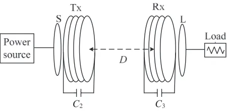
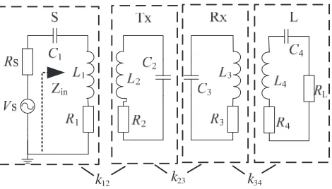
The WPT system is composed of four resonant coils: source, transmission, receiving and load resonant coils, labeled as S, Tx, Rx and L resonant coils, as shown in Fig. 1. All the resonant coils are assumed to be aligned coaxially. Dis the distance between Tx and Rx resonant coils. The WPT system can be represented in terms of lumped circuit elements (Lm,Cm, and Rm(m = 1 (S), 2 (Tx), 3 (Rx), 4 (L))),
as shown in Fig. 2. Lm is the self-inductance of each coil, Cm the compensation capacitor of each coil,
Rm the parasitic resistance of each coil, Vs the source power, Rs the internal resistor of power,RL the
load resistor, RL equal to 50 Ω, and kmn the coupling coefficient betweenm and n resonant coils. The
cross-coupling coefficients are very small, and they can be neglected in the following analysis. ω is the operating angular frequency, ωm the resonant angular frequency of each coil, ω0 the original resonant angular frequency, andZin the input impedance.
C2 C3
Figure 1. The simplified schematic of the WPT system based on magnetically coupling resonator.
By applying Kirchhoff’s voltage law (KVL), the WPT system is presented as follows [10]: ⎧
⎪ ⎨ ⎪ ⎩
Z1I1+jωM12I2=Vs
jωM12I1+Z2I2+jωM23I3= 0
jωM23I2+Z3I3+jωM34I4= 0
jωM34I3+Z4I4= 0
k12 k23 k34
Figure 2. The equivalent circuit model for the WPT system. Each coil is modeled as series resonators.
⎧ ⎪ ⎨ ⎪ ⎩
Z1 =R1+Rs+jωL1+ 1/(jωC1)
Z2 =R2+jωL2+ 1/(jωC2)
Z3 =R3+jωL3+ 1/(jωC3)
Z4 =R4+RL+jωL4+ 1/(jωC4)
(2)
where Im is the current of each coil, and Mmn is the mutual inductance between m and n resonant
coils. According to Eqs. (1) and (2), the efficiency expression is obtained as follows:
η = I 2 4RL
VsI1
= ω
9k2
12k232 k342 QL
64ω2(Q1+Qs)(A2+B2) + 4Q2ω2k212{[−32δ2+ 8ω2k342 + 4Q3(Q4+QL)]2 +[8 (Q4+QL)δ+ 8Q3δ]2}+Q3[4ω6k122 k223δ2+ω6k212k223(Q4+QL)2] +ω9k122 k232 k342 (Q4+QL)
(3)
where
A = Q2Q3δ/4ω2+ (Q2+Q3) (Q4+QL)δ/4ω2−δ3+ω2k342 δ/4 +ω2k232 δ/4
B = Q2Q3(Q4+QL)/8ω3−(Q2+Q3+Q4+QL)δ2/2ω +ωQ2k342 /8 +ω(Q4+QL)k223/8
I1 is the input current. The angular frequency deviation factor is defined as δ = ω0−ω, the unload quality factor of the S coil defined as Q1 = ωL1/R1, the unload quality factor of the Tx coil defined asQ2 =ωL2/R2, the unload quality factor of the Rx coil defined as Q3=ωL3/R3, the unload quality factor of the L coil defined asQ4 =ωL4/R4, the quality factor of power source defined asQS=ωL1/Rs, and the quality factor of load defined asQL=ωL4/RL.
Assumingω1 =ω2 =ω3 =ω4 =ω0, the efficiency expression (3) can be simplified as follows:
η= ULU
2 1U22U32 {(1+Us)(1+UL)+U32+U22(1+UL)
2 +U12
(1+UL)+U32 2
+(1+UL)2U2
1U22+(1+UL)2U12U22U32} (4) where the source matching factor is defined as Us = Rs/R1, the load matching factor defined as
UL =RL/R4, the strong-coupling parameter between S and Tx defined as U1 =k122 Q1Q2, the strong-coupling parameter between Tx and Rx defined as U2 =k223Q2Q3, and the strong-coupling parameter between Rx and L defined asU3 =k234Q3Q4.
By differentiating η with respect toULand equating the differential function to zero
∂η
∂UL = 0 (5)
The load matching factor for the optimum efficiency can be obtained as follows:
UL opt=
[(UsU22+ 2UsU2+U22+Us+ 1 +U1U2+ 2U2)(Us+ 1 + 2UsU1+ 2UsU2
+2UsU1U2+ 3U22+U12U2+ 3U1+ 2U2+U22+UsU22+ 3U1U2+UsU12+U13)]1/2 1 + 2UsU2+ 2U2+Us+U1+U22+U1U2+UsU22
(6)
In order to obtain the optimum efficiency, the optimum load resistorRL opt(influencingUL optin Eq. (6),
3. NEW METHOD FOR FTOE
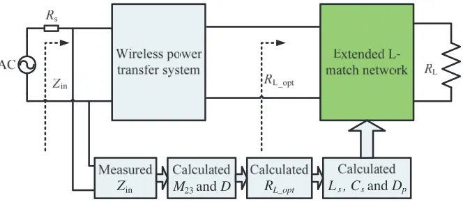
In this section, a fast tracking optimum efficiency method is illustrated with the help of the circuit structure in Fig. 3. The input impedance values Zin can be obtained by measuring the input voltage and input current. M23 value can be calculated by Zin value according to (13). For a given M23, the optimum load resistor RL opt can be obtained according to Eq. (6). The equivalent load resistor can be
adjusted by the L-type matching network. Cs and Cp values in the L-type matching network can be
obtained according to RL opt.
in
Z M 23and D RL_opt L , C s sand Dp
Figure 3. The circuit structure of the FTOE method.
3.1. Estimation of the Transfer Distance D
The transfer distanceD can be represented by the mutual impedanceM23 between Tx and Rx. IfM23 value may be obtained, the transfer distance may be estimated.
The mutual inductance of two coaxial circular current loops can be stated in terms of complete elliptic integrals [20]:
M =μ0 √
RPRS
b
2−b2 K(b)−2E(b) (7) where
b =
4RPRS
h2+ (R
P +RS)2 (8)
K(b) = π/2
0
1
1−b2sin2
θdθ
(9)
E(b) = π/2
0
1−b2sin2θdθ (10)
M is the mutual inductance of two circular loops of radiiRP andRS,hthe distance between loops,K(b)
the complete elliptic integral of the first kind, andE(b) the complete elliptic integral of the second kind. The relationship between the mutual inductance and the distance can be obtained from Eqs. (7)–(10).
M23 value may be obtained by the input impedance. The input impedance is defined as
Zin=Vs/I1−Rs,Zin may then be obtained from Eqs. (1) and (2).
Zin= ω 4M2
12M342 +ω2M122 Z3Z4+ω2M232 Z1Z4+ω2M342Z1Z2+Z1Z2Z3Z4
ω2M2
23Z4+ω2M342Z2+Z2Z3Z4
−Rs (11)
Assuming the system operates in the resonant state, Equation (2) can be simplified as follows:⎧ ⎪
⎨ ⎪ ⎩
Z1 =R1+Rs
Z2 =R2
Z3 =R3
Z4 =R4+RL
Equation (12) is substituted into Equation (11), and Equation (13) can be obtained as follows:
M23=
{ω
4M2
12M342 +ω2M122 R3(R4+RL) +ω2M232(R1+Rs)(R4+RL) +ω2M342 (R1+Rs)R2−(Zin+Rs)[ω2M342 R2+R2R3(R4+RL)]}
(Zin+Rs)ω2(R
4+RL)−ω2(R1+Rs)(R4+RL)
(13)
Zinvalue can be obtained by measuring the input currentI1. M23value can be calculated from Eq. (13) when the parameters of the resonant coils and the load resistor are given. Then, the transfer distance
D can be calculated from Eqs. (7)–(10). The optimum load resistor RL opt can be obtained according
to Eq. (6) under a given transfer distanceD.
3.2. Analysis of the L-Match Network
The impedance matching network is used to automatically change the equivalent load resistor. There are several types of impedance matching networks such as the L-match, Pi-match and DC-DC match networks. All matching networks can match the impedance of the WPT system. The L-match network is simple. Therefore, it is used in this paper. The L-match network includes the L-type and inverted L-type matching networks, as shown in Fig. 4.
C
pR
LR
L_optL
sFigure 4. The circuits of the L-match network.
Figure 4 shows the L-type matching circuit. Using the circuit theory, its equivalent impedance equation can be obtained as follows:
RL−opt=jωLs+ 1 + RL
jωCpRL (14)
The imaginary and the real parts on both sides of Eq. (14) are equal. Equations (15) and (16) can be obtained according to Eq. (14).
Cp =
(RL/RL opt−1)
ω2R2
L
(15)
Ls = CpR
2
L
1 +ω2R2
LCp2
(16)
Cp value can be obtained from Eq. (15) under a givenRL opt. Cp value must be positive. Therefore, RL
value must be larger thanRL opt value. The L-type matching network can be used whenRL> RL opt.
Ls value can be obtained from Eq. (16) under a given RL opt.
3.3. Design of the L-Match Network
The L-type matching network is used becauseRLvalue (RL= 50 Ω) is larger thanRL optvalue. RL opt
is changed as the transfer distance is changed according to Eq. (6). Cp and Ls values are changed as
RL opt is changed according to Eqs. (15) and (16). In order to automatically adjust RL opt,Cp and Ls
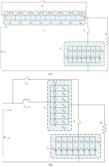
values should be automatically adjusted. Two methods that use the capacitor matrix and inductance matrix are proposed to adjust Cp and Ls values, as shown in Fig. 5. Fig. 5(a) shows the extended
the switch array selection (Spm and Ssm,m= 1–8). Fig. 5(b) shows the extended L-match network of using the capacitor matrix, and the capacitors are connected in parallel according to the switch array selection. The capacitor matrix is used in this paper because it is relatively easy to implement.
When switchS1is on, and switchS2is off, the extended L-match network is bypassed. The transfer
(a)
(b)
distance can be estimated from the previous analysis. The optimum load resistorRL optcan be obtained for different transfer distances. Then, Cp and Ls values are obtained from Eqs. (15) and (16) under a
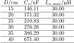
givenRL opt. Table 1 showsCp andLsvalues whenDis ranged from 15 cm to 40 cm. In order to adjust
Ls value, the capacitor matrix (Cs) is connected to Ls in serial. The maximum Ls value is 26.22µH
from Table 1. The allowance ofLs is 20% of the maximumLs. Therefore,Ls maxvalue is set at 30µH.
Cs value can be obtained according to Eq. (17).
Cs= 1
ω2(L
s max−Ls)
(17)
Cs values are shown in Table 2 for different D. Csm value is set at 3×2m−1nF (m = 1–8) in order
to obtain different Cs values. Cpm value is set at 1×2m−1nF (m = 1–8) in order to obtain different
Cp values. When the switch S1 is off, and the switch S2 is on, the L-type matching network is added into the WPT system to change the equivalent load resistor. If the measured input impedance value is changed, switchS1 is on, and switchS2is off. Then the system restarts to estimate the transfer distance (the mutual inductance between Tx and Rx). Once the transfer distance is obtained, the system starts to rematch the equivalent load resistor by adjustingCs and Cp values.
Table 1. Cp and Ls values for different D.
D/cm Cp/nF Ls/µH
15 194.82 12.66 20 160.15 15.21 25 133.22 17.98 30 112.60 20.83 35 97.67 23.44 40 84.60 26.22
Table 2. Cs and Ls max values for differentD.
D/cm Cs/nF Ls max/µH 15 146.11 30.00 20 171.32 30.00 25 210.83 30.00 30 276.26 30.00 35 386.29 30.00 40 671.40 30.00
3.4. The Flowchart of FTOE Method
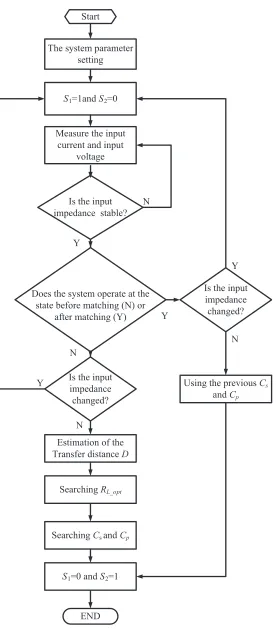
A flowchart of the FTOE method is shown in Fig. 6 and described as follows:
(i) The system parameters, including the input impedance values, optimum load resistor values, Cs
values andCpvalues, are set. First, the input impedance values before matching and after matching are calculated whenDis ranged from 15 cm to 40 cm in a step of 5 cm. Secondly, the optimum load resistor values are calculated whenDis ranged from 15 cm to 40 cm in a step of 5 cm. Thirdly,Cs
and Cp values are also calculated according to the optimum load resistors. Finally, all values are represented in the form of a matrix.
(ii) When switch S1 is on (S1 = 1), and switch S2 is off (S2 = 0), the extended L-type matching network is bypassed.
(iii) The input current and input voltage can be monitored by using current and voltage sensors; (iv) The input impedance can be obtained by the input current and input voltage. We continuously
collect 20 input impedance values. If the condition of Zin(20)–Zin(1)<0.01 is satisfied, the input impedance is stable. Zin(20) is the twentieth input impedance. Zin(1) is the first input impedance. (v) Comparing the current input impedance value with all input impedance values calculated in the first step, the minimum difference Ebef between the current input impedance and all input impedance values before matching can be found; the minimum difference Eaft between the current input impedance and all input impedance values after matching can be found. If the condition of
Ebef < Eaft is satisfied, the system operates at the state before matching. Conversely, the system operates at the state after matching.
Start
The system parameter setting
S1=1and S2=0
Measure the input current and input
voltage
Is the input impedance stable?
Does the system operate at the state before matching (N) or
after matching (Y)
Is the input impedance changed?
Is the input impedance changed?
Estimation of the Transfer distance D
Searching RL_opt
Searching Cs and Cp
S1=0 and S2=1
Using the previousCs
andCp
END Y
N
N
Y
N
Y
N Y
(vii) The transfer distance can be estimated according to the input impedance value. (viii) The optimum load resistor can be found according to the transfer distance.
(ix) Cs andCp values can be found according to the optimum load resistor.
(x) When switch S1 is off (S1 = 0), and switch S2 is on (S2 = 1), the L-type matching network is added into the system.
(xi) When the system operates at the state after matching, we can use the previousCs and Cp values
to match the system.
(xii) If the input impedance is changed, the system restarts to detect the input impedance.
4. SIMULATION RESULTS
To validate the proposed method, the simulation model is built with the help of ANSYS Maxwell and MATLAB. The parameters of the system are shown in Table 3 in Section 5.
(a)
(b)
(c)
4.1. Fixed Transfer Distance
When the transfer distance is fixed at 30 cm, the optimum load resistor can be obtained by the proposed method. In addition, the optimum input impedance can also be found. Fig. 7(a) shows the input impedance values. The system starts to automatically match at the time of 2 ms. It can be seen that the input impedance value before matching is 0.86 Ω, and the input impedance value after matching is 3.89 Ω from Fig. 7(a). Fig. 7(b) shows the input current values. It can be seen that the input current values before matching are larger than those after matching. The input current value before matching is 10.96 A, whereas the input current value after matching is 2.62 A. Fig. 7(c) shows the output voltage values. The output voltage value before matching is 41.1 V, whereas the output voltage value after matching is 31.6 V.
(a)
(b)
(c)
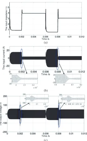
4.2. Varied Transfer Distance
The transfer distance is initially set at 30 cm. Fig. 8(a) shows that the input impedance values versus time. It is clearly seen that the input impedance values are changed as the transfer distance is changed. The system starts to automatically match at the time of 2 ms with D= 30 cm. The input impedance value before matching is 0.86 Ω, and the input impedance value after matching is 3.89 Ω withD= 30 cm. Then it is changed from 30 cm to 25 cm at the time of 6 ms. It can be seen that the input impedance value before matching is 0.54 Ω, and the input impedance value after matching is 3.14 Ω withD= 25 cm. Figure 8(b) shows the input current values versus time. It is clearly seen that the input current values after matching become smaller. The input current value before matching is 10.96 A, whereas the input current value after matching is 2.62 A with D= 30 cm. The input current value before matching is 16.48 A, whereas the input current value after matching is 3.29 A with D= 25 cm. Fig. 8(c) shows the output voltage values versus time. The output voltage value before matching is 41.1 V, whereas the output voltage value after matching is 31.6 V with D = 30 cm. The output voltage value before matching is 48 V, whereas the output voltage value after matching is 36 V withD= 25 cm.
The input power can be obtained by the input current multiplied by the input voltage. And the output power can be obtained by the output voltage (across the load resistor). The efficiency can be obtained by the output power divided by the input power. The efficiency before matching is 29%, and the efficiency after matching is 71% with D = 30 cm. The efficiency before matching is 26%, and the efficiency after matching is 74% with D= 25 cm. It is clearly seen that the optimum efficiency can be tracked by the proposed method.
5. EXPERIMENTAL VERIFICATION
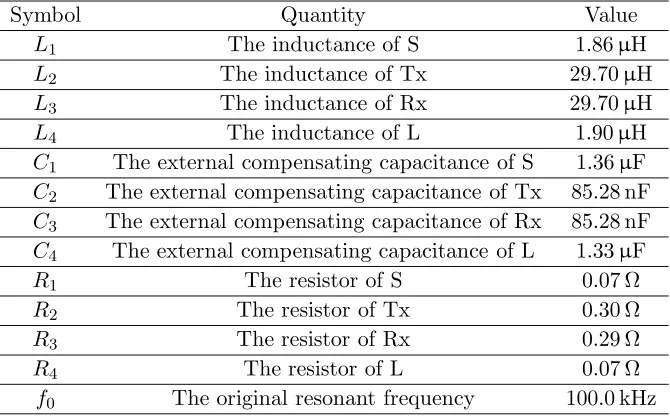
To validate the proposed method, the prototype model of the system is built, as shown in Fig. 9. It is composed of a DC voltage source, four resonant coils, a full-bridge resonant inverter, a extended L-match network and the load. The transmitter on the left consists of a small S coil and a helical Tx resonant coil. The receiver on the right consists of a small L coil and a helical Rx resonant coil. The diameter of the Tx resonant coil is 40 cm with a pitch of 2 cm for approximately 6 turns. The parameters of the Rx coil are the same as those of the Tx coil. The S coil is a single loop and the diameter of the S coil is 50 cm, the parameters of the L coil are the same as those of the S coil. An impedance analyzer is used to extract the parameters in (1). The original resonant frequency is set to be 100 kHz. The parameters of the resonant coils are listed in Table 3.
Table 3. Parameters of the resonant coils.
Symbol Quantity Value
L1 The inductance of S 1.86µH
L2 The inductance of Tx 29.70µH
L3 The inductance of Rx 29.70µH
L4 The inductance of L 1.90µH
C1 The external compensating capacitance of S 1.36µF
C2 The external compensating capacitance of Tx 85.28 nF
C3 The external compensating capacitance of Rx 85.28 nF
C4 The external compensating capacitance of L 1.33µF
R1 The resistor of S 0.07 Ω
R2 The resistor of Tx 0.30 Ω
R3 The resistor of Rx 0.29 Ω
R4 The resistor of L 0.07 Ω
Figure 9. The experimental setup of the system.
Vin
Q1 Q2
Q3 Q4
The full-bridge
Reson tan
resonant inverte
Wire pow trans syst nant
nk
er
eless wer
sfer tem
Exten L-ma netw
nded atch
work RL
Figure 10. The schematic of the resonant inverter.
A full-bridge resonant inverter is used in this paper. Fig. 10 shows the schematic diagram of the inverter. The inverter consists of four switch MOSFETs (Q1 ∼Q4) and a resonant tank [21]. IR2110 and IRF3205 are used as the gate driver and switch MOSFET. The inverter is controlled by the pulse-width-modulation (PWM) signals from DXP28335 controller. An impedance network based on the capacitor matrix is implemented. A total of sixteen group capacitors are used in the capacitor matrix to realize different Cs and Cp configurations. DXP28335 controller periodically monitors the input current and calculates the input impedance. When the input impedance is changed, the controller decides to rematch the impedance network by adjusting Cs and Cp values. The high quality factor capacitors and the relay switches are used to realize the capacitor matrix.
The load resistor is fixed at 50 Ω. We firstly test the reliability of the L-type matching network. Ls,
Csand Cp values are shown in Table 1 and Table 2 for different transfer distances. The equivalent load resistor values can be measured for different combinations of Cs and Cp. Fig. 11 shows RL opt versus
the transfer distanceD. It is clearly seen thatRL opt is changed as Dvaries.
Figure 11. RL opt versusD.
(a)
(b)
(a)
(b)
Figure 13. The input current versus time with D = 25 cm. (a) The input current before matching. (b) The input current after matching.
input current before matching is 16.60 A, whereas the measured input current after matching is 3.51 A. It is clearly seen that the measured input current before matching is larger than that after matching.
Figure 14 shows the calculated and measuredZinbefore and after matching. It can be seen thatZin before matching is smaller than that after matching. Zin is changed as the transfer distance is ranged from 15 cm to 40 cm. Zinbefore matching is ranged from 0.164 Ω to 0.309 Ω, whereas Zinafter matching is ranged from 1.822 Ω to 6.085 Ω.
Figure 15 shows the calculated and measured efficiencies before and after matching. When the impedance matching is not satisfied, the higher the efficiency is, the longer the transfer distance is. However, the maximum efficiency is 30.9% as the transfer distance is varied from 15 cm to 40 cm. When the impedance matching is satisfied, the higher the efficiency is, the shorter the transfer distance is. The maximum efficiency is 72.7% as the transfer distance is varied from 15 cm to 40 cm. The optimum efficiency can be tracked by the proposed method as the transfer distance is changed. It can be seen that the measured efficiency is 77.1%, whereas the simulated efficiency is only 72.7% with D= 15 cm. Although there is 5% power loss on the L-type matching network, the overall efficiency with the L-type matching network is still higher than that without the L-type matching network.
Figure 14. The input impedance versusD. Figure 15. Efficiency versus D.
6. CONCLUSIONS
In this paper, a fast tracking optimum efficiency method is presented. The extended L-type matching network is proposed in order to adjust the equivalent load resistor. The efficiency can be improved for different transfer distances by the proposed method. For example, the efficiency before matching is 27.5%, and the efficiency after matching is 66.8% with D = 30 cm. The optimum efficiency can be tracked automatically as the transfer distance is changed. The efficiency is changed from 66.8% to 70.2% when the transfer distance is changed from 30 cm to 25 cm. The advantage of the proposed method is that the system need not continuously search the optimum Cs and Cp because the transfer distance can be estimated. And the optimum Cs and Cp can be obtained according to RL opt. The number of switches is reduced. Therefore, the proposed method allows for an efficient and robust wireless power transfer system for charging of mobile.
ACKNOWLEDGMENT
This work was supported by the National Natural Science Foundation of China under Grant 61104088 and Grant 51377001. This work was also supported by Hunan Provincial Department of Education under Grant 17C0469.
REFERENCES
1. Kurs, A., A. Karalis, R. Moffatt, et al., “Wireless power transfer via strongly coupled magnetic resonances,” Science, Vol. 317, No. 5834, 83–86, 2007.
2. Karalis, A. J. D. Joannopoulos, and M. Soljaˇci´c, “Efficient wireless non-radiative mid-range energy transfer,”Annals of Physics, Vol. 323, No. 1, 34–48, 2008.
3. Kurs, A., R. Moffatt, and M. Soljacic, “Simultaneous mid-range power transfer to multiple devices,”
Applied Physics Letters, Vol. 96, No. 4, 044102–044102-3, 2010.
4. Chen, J., Z. Ding, and Z. Hu, “Metamaterial-based high-efficiency wireless power transfer system at 13.56 MHz for low power applications,”Progress In Electromagnetics Research B, Vol. 72, No. 1, 17–30, 2017.
6. Shin, J., S. Shin, Y. Kim, et al., “Design and implementation of shaped magnetic-resonance-based wireless power transfer system for roadway-powered moving electric vehicles,”IEEE Transactions on Industrial Electronics, Vol. 61, No. 3, 1179–1192, 2014.
7. Ram Rakhyani, A. K., S. Mirabbasi, and M. Chiao, “Design and optimization of resonance-based efficient wireless power delivery systems for biomedical implants,”IEEE Transactions on Biomedical Circuits and Systems, Vol. 5, No. 1, 48–63, 2011.
8. Choi, S. Y., B. W. Gu, S. W. Lee, et al., “Generalized active EMF cancel methods for wireless electric vehicles,” IEEE Transactions on Power Electronics, Vol. 29, No. 11, 5770–5783, 2014. 9. Wei, X. Z., Z. S. Wang, and H. F. Dai, “A critical review of wireless power transfer via strongly
coupled magnetic resonances,” Energies, Vol. 7, No. 7, 4316–4341, Jul. 2014.
10. Sample, A. P., D. A. Meyer, and J. R. Smith, “Analysis, experimental results, and range adaptation of magnetically coupled resonators for wireless power transfer,” IEEE Transactions on Industrial Electronics, Vol. 58, No. 2, 544–554, 2011.
11. Kim, N. Y., K. Y. Kim, J. Choi, et al., “Adaptive frequency with power-level tracking system for efficient magnetic resonance wireless power transfer,”Electronics Letters, Vol. 48, No. 8, 452–454, 2012.
12. Park, J., Y. Tak, Y. Kim, et al., “Investigation of adaptive matching methods for near-field wireless power transfer,”IEEE Transactions on Antennas and Propagation, Vol. 59, No. 5, 1769–1773, 2011. 13. Duong, T. P. and J.-W. Lee, “Experimental results of high-efficiency resonant coupling wireless power transfer using a variable coupling method,” IEEE Microwave and Wireless Components Letters, Vol. 21, No. 8, 442–444, 2011.
14. Huang, S., Z. Li, Y. Li, et al., “A comparative study between novel and conventional four-resonator coil structures in wireless power transfer,”IEEE Transactions on Magnetics, Vol. 50, No. 11, 1–4, 2014.
15. Fu, M., C. Ma, and X. Zhu, “A cascaded boost-buck converter for high efficiency wireless power transfer systems,”IEEE Transactions on Industrial Informatics, Vol. 10, No. 3, 1972–1980, 2014. 16. Liu, S., L. Chen, Y. Zhou, et al., “A general theory to analyse and design wireless power transfer
based on impedance matching,” International Journal of Electronics, Vol. 101, No. 10, 1375–1404, Oct. 2014.
17. Li, H., J. Li, K. Wang, et al., “A maximum efficiency point tracking control scheme for wireless power transfer systems using magnetic resonant coupling,”IEEE Transactions on Power Electronics, Vol. 30, No. 7, 3998–4008, 2015.
18. Zhong, W. X. and S. Y. R. Hui, “Maximum energy efficiency tracking for wireless power transfer systems,”IEEE Transactions on Power Electronics, Vol. 30, No. 7, 4025–4034, Jul. 2015.
19. Lim, Y., H. Tang, S. Lim, et al., “An adaptive impedance-matching network based on a novel capacitor matrix for wireless power transfer,” IEEE Transactions on Power Electronics, Vol. 29, No. 8, 4403–4413, 2014.
20. Conway, J. T., “Inductance calculations for noncoaxial coils using bessel functions,” IEEE Transactions on Magnetics, Vol. 43, No. 3, 1023–1034, 2007.