Multi-photon polarization
dependence of SSPDs.
THESIS
submitted in partial fulfillment of the requirements for the degree of
BACHELOR OF SCIENCE in
PHYSICS
Author : Jaime S´aez Mollejo
Student ID : s1898450
Supervisor : Michiel de Dood
2ndcorrector : Jan Aarts
Multi-photon polarization
dependence of SSPDs.
Jaime S´aez Mollejo
Huygens-Kamerlingh Onnes Laboratory, Leiden University P.O. Box 9500, 2300 RA Leiden, The Netherlands
June 23, 2017
Abstract
We study superconductivity and photon detection in a NbN nanobridge of 150 nm width and 4 nm thickness. Superconductivity is observed
below Tc =8.4K. The measured critical current as a function of temperature shows a slow decrease up to 7.9 K and more rapid decrease
between 7.9 K and 8.4K. Light counts are only observed below T = 8.4K and dark counts below 7.85K. We characterize the detector by measuring the count rate as a function of polarization and average power to explore a multi-photon polarization dependence. We find a large difference in the response curves of the detector that cannot be explained by a change in the absorption efficiencyη. Unfortunately, at the moment of writing the
origin of the effect is inconclusive and is at least partly caused by a shift in the position of the focused laser beam on the sample when rotating a
Contents
1 Introduction. 1
2 Experimental setup. 3
3 Superconducting properties of the detector. 7
3.1 Critical temperature,Tc. 7
3.2 I-V curves. 9
3.2.1 Discussion. 9
3.3 Ic vs T. 11
3.3.1 Discussion. 11
4 Physics of the detector 13
4.1 Pulse shape of a detection. 13
4.1.1 Discussion. 14
4.2 Light and dark counts as a function of bias current. 14
4.2.1 Discussion. 17
4.3 Role of temperature and bias voltage. 17
4.3.1 Discussion. 18
4.4 Polarization dependence. 20
4.4.1 Tomography. 20
4.4.2 Experimental results. 21
4.4.3 Discussion. 24
5 Conclusions. 27
Chapter
1
Introduction.
Being able to detect single photons is one of the greatest breakthroughs in physics and technology of the last decades with many possible appli-cations. Photomultipliers and avalanche photodiodes are the traditional way to detect single photons but present limitations in their performance. These limitations may be overcome with the development of Supercon-ducting nanowire Single-Photon Detectors (SSPDs) first reported by Gol’tsman et al. [1] in 2001.
The advantages that SSPDs exhibit over other types of single photon detectors are: low dark count rates [2], low jitter, high detection efficiency [3] and a broad spectral range. These characteristics make SSPDs prime candidates for applications such as quantum optics [4], quantum key dis-tribution [5], interplanetary communications [6] or cancer research [7].
SSPDs consist of a thin and narrow strip of a superconducting material cooled down below its critical temperatureTc. A bias current,Ib, compara-ble to the critical current, Ic, is applied to the sample, making possible the transition to the normal state after the absorption of one photon of suffi-cient energy. This transition happens every time that a photon is absorbed, creating a small voltage pulse that is amplified and detected as a count.
2 Introduction.
to extend our understanding to a wider range of energies and to have a better understanding of the detection mechanism.
First experiments in the single photon detection regime point to a po-sition dependent internal detection efficiency [12], in addition to the well-known polarization dependent absorption [13, 14]. An open question is how this polarization dependence persists in the multi-photon regime and if this can further our understanding of the detection mechanism.
Previous tomography measurements [15, 16] were limited in accuracy by power fluctuations in the laser [17]. To resolve this issue we imple-mented a continuous power monitor. For optimum implementation it is necessary to use a power meter with a broad dynamical range (at least 3 orders of magnitude) and low signal to noise ratio for low powers. We also reduced the laser spot size in order to minimize heating of the sample and increase the efficiency of the detector. The reduction of the spot increases the effect of mechanical vibrations of the detector. To mitigate this prob-lem the detector and the rest of the experimental setup were mechanically coupled.
This thesis first introduces in chapter 2 the experimental setup used, followed by a characterization of the superconducting properties of the sample in chapter 3. Chapter 4 is the main part of this report and it is built up from the foundations, what is considered experimentally a detection, aiming to explain the difference in the response of the detector for two different polarizations. Also in this chapter the role of the dark counts is studied and discussed together with the superconducting properties of the NbN.
Chapter
2
Experimental setup.
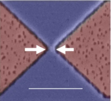
Our nanodetector consists of a deposited granular film of NbN on GaAs substrate with a bow-tie shape, as shown in Fig.2.1. The wire is approx-imately 4nm thin and 150nm wide. The detector is cooled down inside a pulsetube cryostat to∼4.4Kand is kept at a pressure of∼10−7mbar.
The detector is illuminated with a Fianium SC400 supercontinuum pulsed laser with a repetition rate of 20MHzand a pulse width of 20−30ps. The light is filtered by a band pass filter with a center wavelength of 500nm
and a spectral width (FWHM) of 10nm.
At constant temperature a bias current Ib is applied through the super-conductor by means of voltage biasing. Once the bias voltage,Vb, is fixed, the power incident in the sample is changed from ∼ 20nW to ∼ 14µW
with aλ/2 plate between two crossed polarizers (Fig. 2.2). The bias
volt-ageVb is swept in the range where the sample is superconducting and the count rate,CR, of the detector is measured. A secondλ/2 plate is used to
fix the polarization incident on the detector and a 100mmfocal length lens focuses the beam on the sample. A beam splitter is used to deviate part of the laser beam onto a power meter (ThorLabs PM100D) to monitor the power entering in the cryostat.
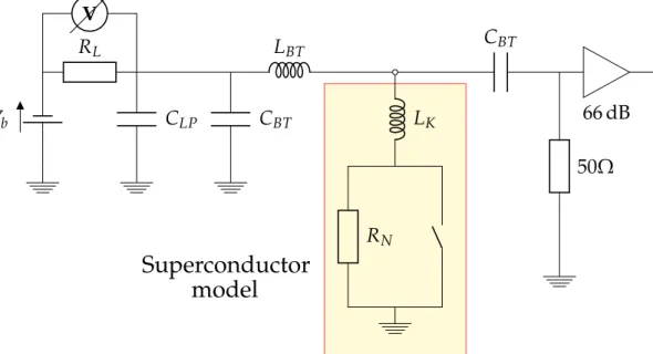
Figure 2.3 shows a schematic drawing of the electronic circuit used to detect photons in the experiment. The circuit can be divided in four parts: a low pass filter (RL andCLP), a bias-T (CBT and LBT), an equivalent elec-tronic circuit of the detector (yellow box) [19] and finally an amplifier. The circuit ensures that the AC noise generated by the voltage source does not reach the NbN detector and once the detector generates a pulse only the high frequency components reach the amplifier.
4 Experimental setup.
Figure 2.1:False color SEM image of a similar detector to the one used. The blue part represent the NbN layer and the red part the GaAs substrate. The narrow bridge pointed with the arrows is the active part of the NbN. The white bar shows the distance of1µmin the sample. Figure taken from [18].
Figure 2.2: Optical setup used to characterize the detector. The two crossed po-larizers and theλ/2plate regulate the transmission asT(θ)∝ cos2(2θ). A beam
splitter allows to monitor the power at all times. The secondλ/2plate changes
the polarization of light and after this is focused on the detector with a100mm focal length lens.
5
The next two capacitors and the inductanceLBTensure that all the high fre-quency components are filtered from the DC bias before reaching the de-tector. The superconductor model is characterized by a kinetic-inductance
LK and two possible states. The switch is closed for the superconducting state (Rsuperconductor = RSC ≈0Ω) and open for the normal state (R= RN). Every time that there is a change from switch closed to switch opened a voltage pulse is generated. Because RL RN, the bias source switches from current bias to voltage bias, greatly reducing Joule heating to allow the detector to self-reset to the superconducting state. The voltage pulse is high pass filtered by CBT and a 50Ω resistor, amplified and sent to a counter (not shown in Fig.2.3).
Vb
V
RL
CLP CBT
LBT
LK
RN
CBT
66 dB
50Ω
Superconductor
model
Chapter
3
Superconducting properties of the
detector.
3.1
Critical temperature,
T
c.
Figure 3.1 presents the measured resistance of the NbN detector as a func-tion of temperature from 260Kto 4.1K. This 2-wire measurement was done with a 612-digit multimeter (Keithley 2000) in the 1MΩregime which ap-plies a test current of 10µA.
As can be seen in the figure, the resistance increases with decreasing temperature until 20K. Below 20Kthe resistance decreases with tempera-ture and below 10K the resistance drops sharply to values R < 1kΩ. At this point, it becomes difficult to measure accurately with the 2-wire mea-surement.
The NbN sample clearly presents a superconductor transition behavior and therefore we aim to estimate the critical temperature,Tc. As a criterion for finding Tc and the width of the transition ∆Tc, we use a linear fit (see line in Fig. 3.1) between the points that represent the 3% and 50% of the maximum resistance. From the fit we obtain a slope(2.09±0.09)MΩ/K. As a result, it takes ∼ 0.3K to go from 3% to 50% of the normal state re-sistance. Taking Tc as the temperature that corresponds to the 25% of the maximum resistance, we estimateTc =8.4±0.2K. It is important to stress that this value ofTc is for a bias current of 10µA.
8 Superconducting properties of the detector.
0
50
100
150
200
250
Temperature (K)
0.0
0.2
0.4
0.6
0.8
1.0
Re
sis
ta
nc
e (
M
Ω
)
7
8
9
10
11
12
13
Temperature (K)
0.0
0.2
0.4
0.6
0.8
1.0
Re
sis
ta
nc
e (
M
Ω
)
Figure 3.1: Resistance of a NbN nanodetector as a function of temperature mea-sured with a test current Ib = 10µA. The red line shows the slope between the
points in which the resistance is between the3%and50%of the maximum resis-tance. Inset: temperature range between7Kand13Kshowing the transition. The critical temperature of this NbN sample isTc =8.4±0.2K. Error bars are smaller
than the symbol size.
3.2 I-V curves. 9
the probability of an electron to pass a grain boundary, Lis the mean free path of the electrons and D the average grain size. Because L decreases with the temperature, the resistance increases. More details can by found in [20] and [21].
3.2
I-V curves.
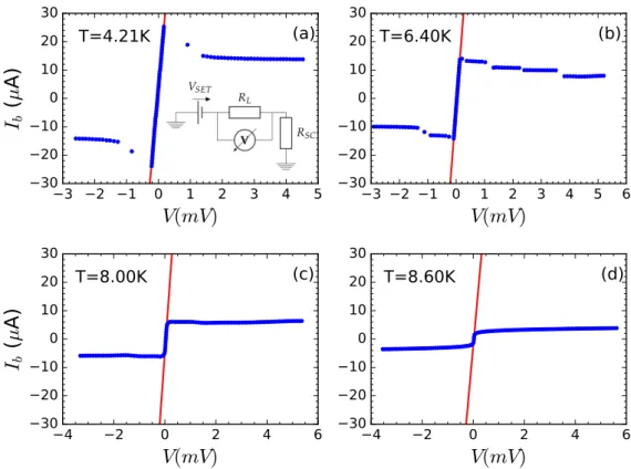
To better characterize and understand the nature of the superconductivity transition in the detector, several I-V curves were measured. Figure 3.2 shows typical I-V curves at different temperatures illustrating the main features. In the experiment the bias voltage is set and the voltage over RL is measured. From this we calculate the voltage over the superconductor, represented as RSC in the inset of Fig.3.2a. All I-V curves present a steep linear part at 0mV and a plateau region for both positive and negative voltages. These plateaus show different characteristics depending on the temperature. From 4.1K to 8.05K the plateaus present a series of discrete decreases in the current. However, from 8.05K the plateau becomes con-tinuous and almost constant. Note the decrease in the critical current of the detector as the temperature is increased.
3.2.1
Discussion.
The I-V curves in Fig.3.2 demonstrate that the NbN sample is supercon-ducting with near-zero resistance. This conclusion is based on the almost vertical line at 0mV in the plots, which indicates that the sample presents zero voltage while a finite amount of current can go through. The red line represented in each plot shows the result of a linear fit, I(V) = RV
0 +I0,
taking into account all the points enclosed by the extremes of the super-conducting region. From 4.1K to 8.60K the parameters of the fit are R0 =
7.9±0.2Ωand I0 =−1±4µA. We attribute this residual resistance to the
fact that the sample is connected in series with resistive wires.
10 Superconducting properties of the detector.
3 2 1 0 1 2 3 4 5
V
(
mV
)
30
20
10
0
10
20
30
I
b(
µ
A)
(a)
T=4.21K
3 2 1 0 1 2 3 4 5 6
V
(
mV
)
30
20
10
0
10
20
30
(b)
T=6.40K
4
2
0
2
4
6
V
(
mV
)
30
20
10
0
10
20
30
I
b(
µ
A)
(c)
T=8.00K
4
2
0
2
4
6
V
(
mV
)
30
20
10
0
10
20
30
(d)
T=8.60K
Figure 3.2: Typical I-V curves of the NbN taken at different temperatures. The lines through the data represent a resistance of7.9±0.2Ω. Error bars are smaller than symbols size. The inset of Fig.(a) shows a schematic circuit explaining how to obtain the voltage of the superconductor.
3.3 Icvs T. 11
3.3
I
cvs T.
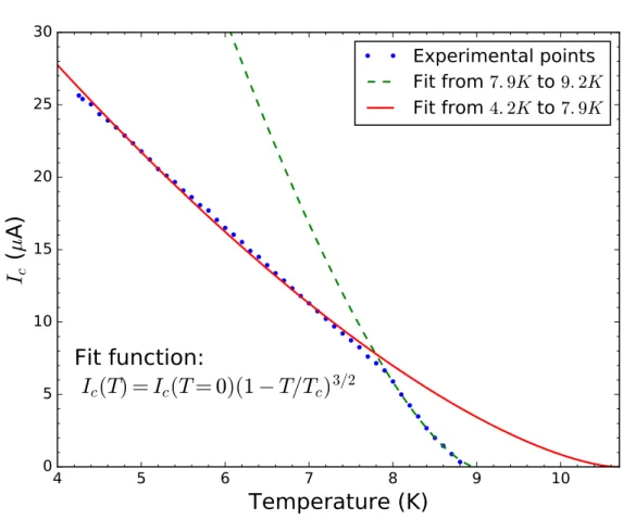
As presented in Fig.3.2, the critical current of the NbN sample decreases as the temperature approaches to Tc. A more detailed study is shown in Fig.3.3 using the measured I-V curves. The critical current plotted for each temperature corresponds to the point where the slope of the I-V curve exceeds a resistance of 66Ω. As can be seen in the figure, the data presents a qualitative change in behavior atT = 7.9±0.1K, where the slope of the curve becomes steeper, dividing the plot in two different regions: T67.9K
and 7.9K <T <9.1K.
3.3.1
Discussion.
The lines in Fig.3.3 correspond to two different fits to the Ginzburg-Landau dependence Ic(T) = Ic(0)(1−T/Tc)3/2 in the regions mentioned before. The parameters of the dashed green fit are Ic(T = 0) = 162±2µA and
Tc = 8.98±0.01K, while in the case of the solid red fit are Ic(T = 0) = 56.2±0.4µAand Tc =10.65±0.04K.
12 Superconducting properties of the detector.
4
5
6
7
8
9
10
Temperature (K)
0
5
10
15
20
25
30
I
c
(
µ
A)
Fit function:
I
c
(
T
) =
I
c
(
T
= 0)(1
−
T/T
c
)
3
/
2
Experimental points
Fit from
7
.
9
K
to
9
.
2
K
Fit from
4
.
2
K
to
7
.
9
K
Figure 3.3: Dependence of the critical current of the sample on the temperature. The plot presents two different regions that are fitted with the Ginzburg-Landau dependence Ic(T) = Ic(0)(1−T/Tc)3/2. The solid/red fit corresponds to the
temperatures between4.1Kand7.9Kand the dashed/green fit corresponds from
7.9K to 9.1K. The parameters of the green fit are Ic(T = 0) = 162±2µA and
Tc = 8.98±0.01K. In the case of the red fit are Ic(T = 0) = 56.2±0.4µA and
Tc =10.65±0.04K. Error bars smaller than symbol size.
Chapter
4
Physics of the detector
We start this chapter by defining what we mean by a count and how the count rate of the detector changes when varying the bias voltage and the temperature. The correlation between the regime change in Fig.3.3 and the lack of light and dark counts above 7.9K is discussed. Section 4.4 ad-dresses the polarization dependence in the multi-photon regime. We find that other factors contribute to the signal and discuss how these could be eliminated.
4.1
Pulse shape of a detection.
In this section we define what is called a detection event. As explained in the introduction, when a photon is absorbed the sample can go through a transition from the superconducting to the normal conducting state. The detection can be understood by modeling the detector using the equiva-lent circuit in the yellow box in Fig.2.3 [19]. The absorption of a photon breaks superconductivity and causes the sample to have a certain resis-tance Rn. Because RL Rn, the bias current Ib through the detector drops, with a time constant τf all = LK/(Rn +50Ω), and causes a volt-age pulse atRL. As soon as Joule-heating, given byRnI(t)2, is sufficiently reduced, the detector cools into the superconducting regime and the Ib through the detector is recovered to its initial value, with the time con-stantτrise = LK/50Ω.
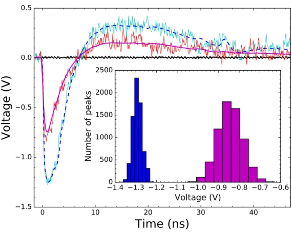
Figure 4.1 shows the typical pulse shape of detection events at a tem-perature of T = 4.2K. The solid magenta and dashed blue lines corre-spond to the average pulse of more than 6900 pulses with bias currents of
14 Physics of the detector
the average pulses correspond to a randomly chosen single pulse for each
Ib/Icratio. The black line shows the average background noise. This back-ground is subtracted from the pulses. The inset represents the distribution of the maximum value of each of the pulses.
These data were measured with an oscilloscope (LECROY WP7300A ) capable of sampling at 3GHz with a trigger level of −0.2V. The voltage pulse was amplified by 3 identical amplifiers (Minicircuits ZX60-3018G-S+) connected in series with a broadband from 20MHzto 3000MHz and total power amplification up to 66dB.
4.1.1
Discussion.
The shape of the pulse in Fig.4.1 shows an initial peak followed by a sec-ondary maximum around 15−20nsas a result of the response of the nan-odetector and the limitations of the electronics.
The pulse shape is limited by the electronics used, in particular by the low frequency cut-off of the amplifiers. The fall time τf all is limited by the sample rate of the oscilloscope and the high frequency cut-off of the amplifiers. It is not possible to register any signal faster than 0.3ns. The rise timeτriseis limited by the amplifiers, which filter the frequencies be-low 20MHz. This filtering from the amplifiers explains why the average pulses become zero at the same point and the signal changes sign.
Every detection from this detector corresponds to pulses with similar characteristics to the ones shown. For the upcoming results the trigger level used for considering a count is−0.2V (or 0.2V in case of having the inverse polarity). In our experiment there are no counts if there are no pulses with a height larger than 0.2V.
4.2
Light and dark counts as a function of bias
current.
The next step in characterizing the detector is measuring how the count rate,CR, depends on the bias current Ib.
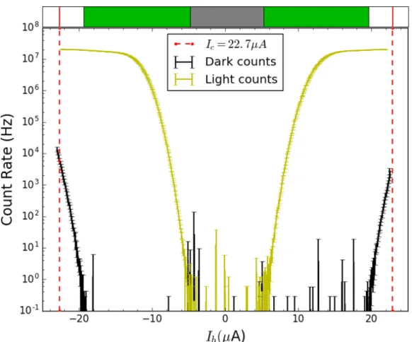
Figure 4.2 presents the dark count rate (black symbols) and light count rate (yellow symbols) as function of applied bias current for a temperature of 4.5K. Dark counts were measured with the detector in complete dark-ness covering the entrance of the cryostat with an aluminum lid. Light counts were measured illuminating the detector with a constant laser power of∼10µWat a wavelength of 500nm.
4.2 Light and dark counts as a function of bias current. 15
0
10
20
30
40
Time (ns)
1.5
1.0
0.5
0.0
0.5
Voltage (V)
1.4 1.3 1.2 1.1 1.0 0.9 0.8 0.7 0.6
Voltage (V)
0
500
1000
1500
2000
2500
Number of peaks
Figure 4.1:Amplified voltage pulse at4.2Kfor two different bias currentsIb. The dashed blue line represents the average pulse for Ib/Ic ≈ 0.92and the magenta
line is the average pulse forIb/Ic ≈0.81. The curves on top of the average pulses
are single pulses at the mentioned Ib/Ic ratio in each case. Inset: Distribution of
the highest point of each single pulse, corresponding the colors to the sameIb/Ic
16 Physics of the detector
Figure 4.2: Response of the detector atT = 4.5Kas function of the bias current. The dark counts present an exponential dependence onIb. The light counts show a similar exponential behavior until12µAwhere the detector starts saturating to
the pulse rate of the laser illuminating with a power of∼ 10µW. The vertical
dashed lines indicate the critical current of the superconductor.
4.3 Role of temperature and bias voltage. 17
As can be seen from the figure, the light counts are present for currents exceeding±5µAand increase by 8 orders of magnitude until a count rate
∼ 2·107Hz is reached, a value that coincides with the pulse rate of the laser. The currents which do not present light counts are represented by the grey color in the colorbar on top of the plot. Dark counts are only mea-surable for currents above±20µA(Ib/Ic =0.87) and show an exponential dependence on current until Ic. The colorbar shows the absence of dark counts with green and grey colors.
Above Ic, the count rates registered are of the order of 108, with the detector operating in the relaxation-oscillation regime. The data for Ib >
Ic are not presented in Fig.4.2. The white part of the colorbar above Ic presents the relaxation-oscillation regime and contains a mix of dark and light counts.
4.2.1
Discussion.
The dark counts are temporary transitions to the normal conducting state of the sample. The voltage pulse cannot be distinguished from that of light counts. The exponential regime of dark counts is consistent with the results of [24] and [23], which suggest that these fluctuations are the con-sequence of current-assisted thermal unbinding of vortex and anti-vortex pairs (VAP), in the context of the Berezinskii-Kosterlitz-Thouless (BKT) transition. This BKT transition is a 2D phase transition which appears at a critical temperatureTBKT, below theTc of the superconductor, and hap-pens when a characteristic dimension (e.g. width) of the superconducting sample is comparable with the coherence length of the superconductor,
ζ(T). We associate the different regimes in the observed IC(T) with this BKT transition. BelowTBKT the vortex and anti-vortex pairs are bounded. For temperatures betweenTBKT and TCthe vortices are free.
In the case of light counts, the results exhibit a larger sensitivity to the laser pulses for currents closer to the critical current. Moreover, the count rate measured is always at least 3 orders of magnitude larger than the dark count rate and atT =4.5Kthere is a wide range of Ib without dark counts (green area in the colorbar).
4.3
Role of temperature and bias voltage.
18 Physics of the detector
temperatures and Vb the dark counts disappear. In order to understand the limitations of the detector, we need to investigate the nature of the de-tection mechanism and the origin of dark counts. Hence, we measured the dependence of the count rate for light counts and dark counts as a function of both bias voltage and temperature.
In this section count rate equals zero means that no counts where mea-sured with a count rate larger than 1Hz and an amplified voltage pulse larger than 200mV. The detector was illuminated with∼12µW.
Figure 4.3 shows a false color plot of the count rate as a function of temperature and bias voltage, using the same color code as the colorbar in Fig.4.2 (grey: zero counts for dark and light events. Green: no dark count events. White: non-zero light and dark counts). Blue circles present the critical current of the superconductor (right vertical axis), indicating the area where the sample is in the superconducting state. The solid red line and the black dashed line present the same fits as in Fig.3.3.
The grey region shows that above 8.4±0.1K the detector is not sensi-tive to any kind of detection event for the temperatures and the bias volt-ages measured. The green color presents a symmetric behavior consider-ingVb = 0mV as axis and the green contour from 4.5Kto 7.3Kpresents a linear relation forVb and the temperature. The blue points and the green area intersect at 7.85±0.05K (solid black line), above this temperature there are no dark counts registered for the superconducting state, while there are counts for Vb > 0.7mV and Vb < −0.7mV. Above 8.05±0.05K the sample does not present measurable dark counts for anyVb.
4.3.1
Discussion.
Figure 4.3 provides information about the process that produces the dark counts. It can be deduced that the activation of the dark count mechanism depends on temperature andVb. At a fixedVb between 2mV and 1mV (or
−2mV and −1mV) the count rate is zero until a temperature, where the dark count mechanism is activated. We associate this effect to the thermal excitations that produce the unbinding of the vortices [24]. The disap-pearance of the dark counts in the superconducting state at 7.85±0.05K
coincides with the change of regime at 7.9±0.1K in Fig.3.3. These two findings need to be interpreted with caution because our research does not demonstrate a direct correlation between the lack of dark counts and the deviation of the critical current data from the Ginzburg-Landau expres-sion for Ic(T). Above 8.05±0.05Kthe count rate becomes zero for all the measuredVb, which means that the dark count mechanism is completely
4.3 Role of temperature and bias voltage. 19
4.5
5.0
5.5
6.0
6.5
7.0
7.5
8.0
8.5
Temperature (K)
3
2
1
0
1
2
3
V
bias(
m
V
)
25
20
15
10
5
0
5
10
15
20
25
I
b(
µA
)
20 Physics of the detector
deactivated. One possible interpretation of this result is that the nature of dark count events goes beyond the pure superconducting state.
Figure 4.3 also shows that for a fixed temperature, there is a bias volt-age Vb at which the dark count events are not zero anymore. This bias voltage is close to a linear relation as a function of the temperature be-tween 4.5Kand 7.3K.
The grey region shows where the detector is not sensitive when it is illuminated with∼12µW. The highest temperature at which the detector
is sensitive to light is 8.4±0.1K. The data shows that the detector is sen-sitive to photons above 7.9K, where the change of regime of Ic(T)occurs and directly answers the question of subsection 3.3.1.
The white area between the critical current and the green area presents a count rate for light counts and dark counts below or equal to the pulse rate of the laser. The white area beyond the critical current of the supercon-ductor presents count rates larger than the pulse rate of the laser (20MHz), which corresponds with the relaxation-oscillation regime [22].
4.4
Polarization dependence.
4.4.1
Tomography.
In a simplified picture, the detector can click or not click when it is illu-minated. The count rate is the only observable that we can measure but does not contain information about the number of photons absorbed. To understand the detection mechanism of the detector it is necessary to find a method which gives a connection between count rate and absorbed pho-tons. Quantum detector tomography is the process which connects the two by the calculation of the Positive Operator Valued Measure [25].
Quantum detector tomography [15, 17] is used to understand the quan-tum response of the detector to different quanquan-tum states, in our case dif-ferent Fock states or photon number states from count rate statistics using coherent states generated by the laser. Attenuating the power of the laser allows to tune the average photon number of the coherent states. Once the response of the detector to different photon distributions is measured, quantum tomography can convert this result to the response of the detec-tor to detect a certain number of photons.
The click probability of the detector is given by:
Rclick(N) =1−e−ηN m
∑
i=0
(1−pi)
(ηN)i
i! (4.1)
4.4 Polarization dependence. 21
where N is the mean photon number of the coherent state, η is the
effective absorption efficiency which describes the optical coupling and
pi is the detection probability thati absorbed photons cause a click. This expression assumes that η 1 and that when the detector is saturated
pi =1 fori >m. Also we considerp0 = 0 because the click probability to
detect zero photons is zero. Hence, dark counts are not considered in this equation.
One important property of equation 4.1 is the possibility to separate η
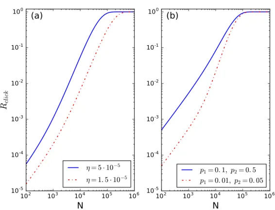
and pi [17]. This is illustrated in Fig.4.4. Figure 4.4a shows the difference between the click probability due to differentη: the response has the same
shapes but is shifted along the horizontal axis. Figure 4.4b presents the response for the sameηbut different detection probabilitiespi. In the latter case the curves present a different shape and cannot be rescaled via the effective absorptionη.
The absorption presented by the NbN nanowire varies with polariza-tion because the asymmetry of the wire imposes different boundary condi-tions and as a result different absorption [14]. This effect is well-understood and leads to a change inη. In addition, the detection probabilities pi are polarization dependent, which implies that the detection mechanism it-self is polarization dependent [12]. If the response of the detector for per-pendicular and parallel polarization is just a difference in the absorption, both curves will have the same shape but will be shifted (ηk 6= η⊥ and
pik = pi⊥). If the detection probabilities pi depends on polarization, a difference in the shape of the curves must be visible (pik 6= pi⊥).
4.4.2
Experimental results.
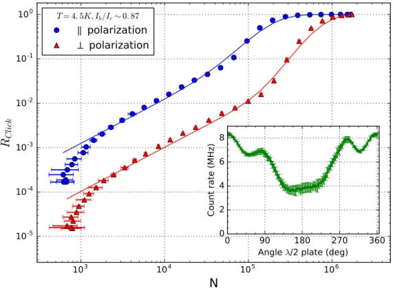
Figure 4.5 shows the response of the polarization for perpendicular (red triangles) and parallel polarization (blue circles) for a bias current of Ib = 20.4±0.2 (Ib/Ic ≈ 0.87) at 4.5K. The horizontal axis corresponds to the average number of photons per pulse, N = (Pλ)/(f hc), where P is the
power illuminating the detector,λthe wavelength of light, f the pulse rate
of the laser, hPlanck’s constant andc the speed of light. The vertical axis is the click probability RClick, which is obtained by dividing the measured count rate by the pulse rate of the laser.
22 Physics of the detector
10
210
310
410
510
6N
10
-510
-410
-310
-210
-110
0R
click
(a)
η
= 5
·10
−5η
= 1
.
5
·10
−510
210
310
410
510
6N
10
-510
-410
-310
-210
-110
0(b)
p
1= 0
.
1
, p
2= 0
.
5
p
1= 0
.
01
, p
2= 0
.
05
Figure 4.4:Click probability calculated with equation 4.1. Fig.(a): Click probabil-ity with same pi values (p1 = 0.01, p2 = 0.5, pi>2 = 1) and different values for
η. Both curves present the same shape and lie on top of each other if are shifted.
Fig.(b): Click probability forη=5·10−5and differentpivalues. The red and blue
lines show a different shape and it is not possible to overlap them modifying the value ofηof one of the curves.
4.4 Polarization dependence. 23
10
310
410
510
6N
10
-510
-410
-310
-210
-110
0R
Click
T= 4.5K, Ib/Ic∼0.87
polarization
polarization
0
90
180
270
360
Angle
λ/2 plate (deg)
0
2
4
6
8
Count rate (MHz)
Figure 4.5: Response of the detector for parallel polarization (blue circles) and perpendicular polarization (red triangles). The blue and red lines correspond to manual fits of the expression 4.1. Inset: Count rate as function of the angle of the secondλ/2plate (Fig.2.2) at constant power. The results show that the count rate
differs by a factor of 2 betweenθλ/2 =0
◦ and
θλ/2 =180
24 Physics of the detector
4.4.3
Discussion.
We attribute the roll-off belowN ∼103 to the limitation of the power me-ter used for monitoring the power that cannot measure the lowest powers accurately. The roll-off can be explained by a small background or dark current that we cannot correct for in the current experiment. We do not consider these points when quantifying the response of the detector. The NbN sample is capable of detecting these low powers, and shows that there is room for improvement if a power meter with broader dynamical range is used. Once this problem is fixed, the next limitation will be set by the extinction ratio of the polarizers used, which limits the power range to approximately 5 orders of magnitude.
To quantify the differences between the two responses, manual fits to equation 4.1 are presented by the solid lines. The values for parallel po-larization are ηk = 1.5·10−5, pk1 = 0.08, pk2 = 0.11, pki>2 = 1 and for
perpendicular polarization areη⊥ = 5.15·10−6, p⊥1 = 0.02, p⊥2 = 0.03, p⊥3 = 0.07 and pi>3 = 1. According to this result, the absorption of the
nanowire is different to both polarizations as expected because ηk 6= η⊥
but also the detection efficiencies are different, pki = p⊥i. Further
exper-iments show that extreme caution must be exercised in the interpretation of these results.
In order to check that the different response in Fig.4.5 is indeed caused by a change of polarization, the count rate as a function ofθλ/2 (angle of
the secondλ/2 plate) for constant power was measured (inset of Fig.4.5).
The count rate for θλ/2 = 0
◦ and
θλ/2 = 180
◦ should be identical. The
inset of Fig.4.5 shows a factor 2 difference in the count rate that can be explained by small deviations of the beam while rotating the λ/2 plate.
According to the manufacturer the beam deviation is≤10arcsec, which in our experimental set up could lead to a deviation of≤ 4.8µm.
Consider-ing a gaussian beam, the diameter of the spot on the sample is ∼ 30µm,
producing a shift of the spot on the sample of∼16% of the spot size. This variation of the position of the spot on the sample could lead to a differ-ent intensity illuminating the detector and as a consequence a differdiffer-ent photon number distribution. If this is the case, the response of the two po-larizations could not be directly compared. The probable deviation of the beam caused by theλ/2 plate would also affect our firstλ/2 plate used to
attenuate the power (Fig.2.2). This hypothesis is also consistent with the fact that the response of the detector depends on the experimental method used to optimize the number of counts.
Several methods can be used to reduce the effect of the deviation. Pre-viously a much larger beam size was used to make the setup less sensitive
4.4 Polarization dependence. 25
Chapter
5
Conclusions.
We have presented the importance of temperature and bias voltage in the activation and deactivation mechanism of the dark counts as well as in the sensitivity of the detector. Our results present a lack of dark counts in the superconducting state atT =7.85±0.05Kand the complete deactivation of the dark counts mechanism above 8.05±0.05K for count rates larger than 1Hz and amplified voltage pulses larger than 200mV. A change of regime was found in the Ic(T) dependence at 7.9±0.1K, close to the dis-appearance of the temperature where the dark counts disappear in the superconducting state.
We have successfully introduced a continuous power monitor and iso-lated mechanical vibrations in the experimental setup. These two im-provements will allow an improved accuracy of the measurements. In addition a reduced size of the beam spot is used to strongly reduce the undesired effects caused by local heating.
Acknowledgements.
I would like to thank Michiel for all the advice, intriguing and fascinating scientific conversations and helping me to do my first steps in research. I really appreciate all the time we spent together in the lab and in front of the whiteboard. I am really grateful for having the opportunity of doing my bachelor project with you. I also want to thank Daan for all the help, advice and teamwork during these months.
Quiero agradecer a mis familiares y amigos, en especial a los que llevo en el camino, todo el apoyo y cari ˜no que siempre me han dado.
References
[1] G. N. Gol’tsman, O. Okunev, G. Chulkova, A. Lipatov, A. Se-menov, K. Smirnov, B. Voronov, A. Dzardanov, C. Williams, and R. Sobolewski,Picosecond superconducting single-photon optical detector, Applied Physics Letters79, 705 (2001).
[2] T. Yamashita, S. Miki, K. Makise, W. Qiu, H. Terai, M. Fujiwara, M. Sasaki, and Z. Wang,Origin of intrinsic dark count in superconduct-ing nanowire ssuperconduct-ingle-photon detectors, Applied Physics Letters99, 161105 (2011).
[3] F. Marsili, V. B. Verma, J. A. Stern, S. Harrington, A. E. Lita, T. Gerrits, I. Vayshenker, B. Baek, M. D. Shaw, R. P. Mirin, and S. W. Nam, Detect-ing sDetect-ingle infrared photons with 93% system efficiency, Nature Photonics
7, 210 (2013).
[4] C. Zinoni, B. Alloing, L. H. Li, F. Marsili, A. Fiore, L. Lunghi, A. Ger-ardino, Y. B. Vakhtomin, K. V. Smirnov, and G. N. Gol’tsman, Single-photon experiments at telecommunication wavelengths using nanowire su-perconducting detectors, Applied Physics Letters91, 031106 (2007).
[5] R. Collins, R. Hadfield, V. Fernandez, S. Nam, and G. Buller,Low tim-ing jitter detector for gigahertz quantum key distribution, Electronics Let-ters43, 180 (2007).
[6] D. M. Boroson and B. S. Robinson, The Lunar Laser Communication Demonstration: NASAˆas First Step Toward Very High Data Rate Support of Science and Exploration Missions, Space Science Reviews 185, 115 (2014).
Had-32 REFERENCES
field,Singlet oxygen luminescence detection with a fiber-coupled supercon-ducting nanowire single-photon detector, Optics Express21, 5005 (2013).
[8] A. D. Semenov, G. N. Gol’tsman, and A. A. Korneev,Quantum detec-tion by current carrying superconducting film, Physica C: Superconduc-tivity351, 349 (2001).
[9] A. Semenov, A. Engel, H.-W. H ˜AŒbers, K. Il’in, and M. Siegel, Spec-tral cut-off in the efficiency of the resistive state formation caused by absorp-tion of a single-photon in current-carrying superconducting nano-strips, The European Physical Journal B47, 495 (2005).
[10] L. N. Bulaevskii, M. J. Graf, and V. G. Kogan, Vortex-assisted photon counts and their magnetic field dependence in single-photon superconduct-ing detectors, Physical Review B85, 014505(2012).
[11] A. N. Zotova and D. Y. Vodolazov, Photon detection by current-carrying superconducting film: A time-dependent Ginzburg-Landau ap-proach, Physical Review B85, 024509(2012).
[12] J. J. Renema, Q. Wang, R. Gaudio, I. Komen, K. op t Hoog, D. Sahin, A. Schilling, M. P. van Exter, A. Fiore, A. Engel, and M. J. A. de Dood,
Position-Dependent Local Detection Efficiency in a Nanowire Supercon-ducting Single-Photon Detector, Nano Letters15, 4541 (2015).
[13] V. Anant, A. J. Kerman, E. A. Dauler, J. K. W. Yang, K. M. Rosfjord, and K. K. Berggren, Optical properties of superconducting nanowire single-photon detectors, Optics Express16, 10750 (2008).
[14] E. F. C. Driessen, F. R. Braakman, E. M. Reiger, S. N. Dorenbos, V. Zwiller, and M. J. A. de Dood, Impedance model for the polarization-dependent optical absorption of superconducting single-photon detectors, The European Physical Journal Applied Physics47, 10701 (2009).
[15] J. J. Renema, G. Frucci, Z. Zhou, F. Mattioli, A. Gaggero, R. Leoni, M. J. A. de Dood, A. Fiore, and M. P. van Exter, Modified detector to-mography technique applied to a superconducting multiphoton nanodetec-tor, Optics Express20, 2806 (2012).
[16] J. J. Renema, G. Frucci, Z. Zhou, F. Mattioli, A. Gaggero, R. Leoni, M. J. A. de Dood, A. Fiore, and M. P. van Exter,Universal response curve for nanowire superconducting single-photon detectors, Physical Review B
87(2013).
REFERENCES 33
[17] Q. Wang, J. J. Renema, A. Gaggero, F. Mattioli, R. Leoni, M. P. van Exter, and M. J. A. de Dood,How noise affects quantum detector tomog-raphy, Journal of Applied Physics118, 134501 (2015).
[18] J. J. Renema, The physics of nanowire superconducting single-photon de-tectors, PhD thesis, Leiden University, 2015.
[19] A. J. Kerman, E. A. Dauler, W. E. Keicher, J. K. W. Yang, K. K. Berggren, G. Gol’tsman, and B. Voronov,Kinetic-inductance-limited re-set time of superconducting nanowire photon counters, Applied Physics Letters88, 111116 (2006).
[20] J. Tyan and J. T. Lue,Grain boundary scattering in the normal state resis-tivity of superconducting NbN thin films, Journal of Applied Physics75, 325 (1994).
[21] A. Nigro, G. Nobile, M. G. Rubino, and R. Vaglio, Electrical resistiv-ity of polycrystalline niobium nitride films, Physical Review B 37, 3970 (1988).
[22] Z. Z. Zhou,Multi-photon detection with superconducting nanowires, PhD thesis, Technische Universiteit Eindhoven, 2014.
[23] J. Kitaygorsky, I. Komissarov, A. Jukna, D. Pan, O. Minaeva, N. Kau-rova, A. Divochiy, A. Korneev, M. Tarkhov, B. Voronov, I. Milostnaya, G. Gol’tsman, and R. Sobolewski,Dark Counts in Nanostructured NbN Superconducting Single-Photon Detectors and Bridges, IEEE Transactions on Applied Superconductivity17, 275 (2007).
[24] A. Engel, A. Semenov, H.-W. H ˜AŒbers, K. Ilˆain, and M. Siegel, Fluc-tuation effects in superconducting nanostrips, Physica C: Superconduc-tivity and its Applications444, 12 (2006).