RFID Techniques for
Passive Electronics
Senior Project
By
Ryan Behr
David Cobos
Electrical Engineering Department
California Polytechnic State University
San Luis Obispo
2011
Table of Contents
Section
Page
List of Tables and Figures……….IV
Acknowledgements……….VI
I.
Introduction………7
II.
Background……….8
III.
Requirements……….10
IV.
Design………..11
4.1
Theory of Operation……….……….11
4.2
Inductors………14
4.3
Circuit Design……….15
V.
Development and Construction……….……24
VI.
Integration and Testing………29
VII.
Conclusion and Recommendations……….33
VIII.
Bibliography……….35
Appendices
A.
Parts Lists and Costs………..36
B.
Time Allocation Estimates……….36
C.
Derivation of Operating Principle……….…37
D.
Picture of Prototype………..40
List of Tables and Figures
Tables
Page
1.
Parts List and Cost………..…36
2.
Schedule – Time Estimates………36
Figures
1.
Schematic of Magnetically Coupled Inductors with Split Supply
Rectification……….11
2.
Pot Core……….15
3.
Coil Wire and Pot Core……….………15
4.
Insufficient V
eeVoltage with NMOS Substrate Internally
Grounded……….….18
5.
Full Schematic of Final Circuit……….…20
6.
Supply Voltages Across Split Supply Capacitors……….20
7.
Modulating Signal on Primary Coil………..21
8.
Output of Envelope Detector………..21
9.
Output of Low-‐pass Filter………..22
10.
Output of Amplification Stage………22
11.
Screenshot of Inductance Calculator Used………24
13.
Smith Chart Plot of 6.197µH Secondary Inductor……….27
14.
Primary (Left) and Secondary (Right) Inductors Used in Final
Circuit………..27
15.
Channel 1 (Top) Signal Across Primary Inductor; Channel 2
(Bottom) Voltage Across VCO……….29
16.
Channel 1 (Top) Showing the Output of the VCO; Channel 2
(Bottom) Showing the Output of Low-‐pass Filter……….31
17.
Channel 1 (Top) Showing the Output of the VCO; Channel 2
(Bottom) Showing the Output of the Amplification Stage…….31
18.
An Equivalent T Circuit with an Open Load………37
19.
An Equivalent T Circuit with a Short Load………..38
20.
Picture of Prototype………..40
Acknowledgements
We would like to thank Dr. Prodanov for his endless
patience and assistance throughout the duration of this
project.
I. Introduction
Magnetic coupling refers to a phenomenon that results when two
conductors are arranged in such a way, such that, when electric current flowing
through one of the conductors changes it results in an induced voltage on the other
conductor via the magnetic field produced by the current changing conductor. The
coupling between two wires can be increased by winding them into coils and placing
them close together on a common axis, so the magnetic field of one coil passes
through the other coil. This phenomenon is a product of electromagnetic induction,
in which, as explained by Faraday’s Law, a time-‐varying current in one coil produces
a time-‐varying magnetic field which produce currents in the receiving coil. In
actuality, the time-‐varying magnetic field produces an electric field that circulates
around the time-‐varying magnetic field. It is this induced electric field that applies a
force on the free electrons in the receiving coil, thus generating electric current.
This principle forms the basis of a seemingly infinite array of applications within the
field of electrical engineering, and specifically as it pertains to this project, wireless
energy transfer and data transmission.
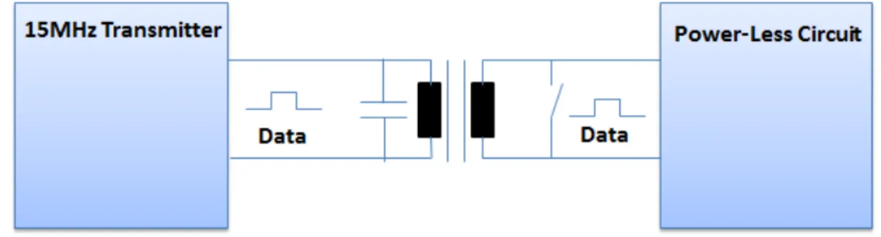
II. Background
The goal of this project is to implement a wireless system which is capable of
wirelessly transferring power to, and receiving data from a passive electronic sensor.
More specifically, to design and test a circuit that will wirelessly harvest power for
circuit operation and transmit sensor data back to the power source for signal
readout. The type of sensor to be used will be a passive digital tire pressure senor.
The sensor must be small in physical size and capable of being inserted on the inner
wall of a vehicle tire. A passive device is one without a battery or an external power
supply. LT Spice will be used as a simulation tool in devising and optimizing a circuit
capable of this type of communication. The circuit will utilize magnetically coupled
coils that function as antennae to supply power as well as transmit data. The
primary, or source coil, will be connected to a signal generator that generates an
alternating current. The secondary coil will be connected in a circuit topology using
two diodes with opposing polarity, and two capacitors to rectify the alternating
signal into two DC voltages. The fundamental principle that this circuit relies on for
operation is the ability to change the impedance seen by the signal generator on the
circuiting the secondary coil. A switch will be placed across the terminals of the
secondary coil, and the state of the switch, whether it is open or closed, will
determine the impedance to the signal generator on the primary side by modulating
the magnetic field of the coupled coils. Varying the impedance seen by the source
effectively modulates the signal on the primary coil. The voltage across the primary
coil should switch between two levels, the different voltage levels can be used as
different logic levels, and binary data can be obtained. Implicit in this theory is the
sensor output must be digital data, as opposed to an analog signal, and the digital
output must be capable of toggling the switch across the secondary coil. The binary
data obtained from the primary coil can be interpreted and readout in any desired
fashion.
III. Requirements
The end goal of this project is to design and test a circuit that will operate at
15MHz and wirelessly harvest power for a digital tire pressure sensor, and transmit
sensor data back to the power source for pressure data readout. In order to
accomplish such an undertaking the following objectives must be met:
1. Design, construct, and characterize coils to function as antennae at 15MHz
2. Construct a full-‐wave rectifier to be used in a split supply fashion
3. Generate a clock signal on the secondary side to operate the sensor and
transmit data at a chosen low frequency in the kilohertz range
4. Implement a bilateral switch to open and short the secondary coil
5. Connect an envelope detector circuit to the primary coil to obtain the
amplitude modulated signal from the 15MHz carrier signal
IV. Design
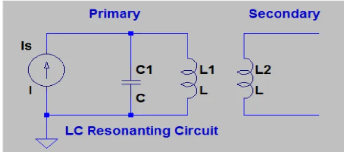
4.1 Theory of Operation
By placing two inductors in close proximity on a common axis a constant
frequency can be transmitted from the primary side inductor to the sensor side
inductor. Inserting two diodes in parallel with opposing polarity and adding a
capacitor in series with each diode creates two DC voltage rails which can be used to
supply power to the sensor network. To maximize the voltage difference across the
rails a split supply is used, this means one rail is positive and the other negative with
respect to ground. Figure 2 below can be used to gain an intuition of the proposed
operation.
In reference to Figure 2, using near-‐field coupling the alternating current
supplied to the primary coil is transmitted to the secondary coil. Vcc would have
2.5V positive with respect to the reference ground voltage, and Vee would have 2.5V
negative with respect to the reference ground voltage. So the voltage difference
across terminals Vcc and Vee is 5V and it would be used to supply power to the digital
sensor part number MPL115A1.
The driving source of the primary coil operates at a frequency of 15MHz.
This frequency was selected for multiple reasons. This particular frequency lies
within the industrial, scientific, and medical (ISM) radio band, an internationally
reserved frequency range for industrial, scientific, and medical purposes other than
communications. Additionally, system functionality relies on the ability to induce a
voltage in the secondary coil via the primary inductor. The voltage across the
primary inductor, V1, and the voltage induced across the secondary inductor, V2, is
given by the following relations:
V1 = ωL1I1COS(ωt + 90°) (1)
V2 = ωk !1!2I1COS(ωt + 90°) (2)
where k is the coupling coefficient between the two inductors, ω is the angular
frequency of the system, I1 is the magnitude of the current in the primary inductor,
and L1 and L2 are the inductor values in Henries. What is to be derived from the
above equations is the fact that V2 increases as the frequency increases, so using the
demands across the secondary coil, while not requiring excessive voltage and
current in the primary inductor.
Not shown in Figure 2 is a switch placed across the terminals of the
secondary coil. The function of the switch is to change the impedance seen by the
driving source on the primary side. Changing the load presented to the primary side
requires L2 to vary. L2 is effectively short circuited when the switch is closed,
resulting in a different inductance seen at the primary side, which will be called Lseen.
When small current is drawn from the capacitors, little current is drawn through the
diodes, and L2 is effectively open circuited. The state of the switch, open or closed,
will be determined by the output of the sensor, and since the sensor outputs digital
data the varying load will fluctuate between two distinct levels. The inductance
seen at the primary side, Lseen, is expressed in the following equations:
secondary is open circuited: Lseen = L1 (3)
secondary is short circuited: Lseen = L1(1-‐k!) (4)
where again k is the coupling coefficient between the two coils. It is important to
note that short circuiting the secondary coil does not discharge the capacitors, the
charge on the capacitors is held captive due to the diodes being reversed biased,
short circuiting only changes the impedance seen by the driving source. Varying the
impedance presented to the signal generator on the primary side modulates the
voltage presented to the primary coil. Modulation on the primary inductor enables
Figure 3: Secondary circuit when switch is ON
Figure 4: Secondary circuit when switch is OFF
4.2 Inductors
In an effort to reduce the overall size of the passive sensor the inductors
must be very small. Designing an inductor to function as an antenna eliminates
toroid cores from being used. For this application pot core inductors are ideal. A
pot core, pictured below in Figure 6, is round with an internal hollow that almost
completely encloses the coil. In the center of the hollow is a bobbin which the coils
are formed around. The advantage of a pot core is the shielding effect provided by
the outer rim which acts to prevent radiation and electromagnetic interference.
Furthermore, the magnetic flux radiates solely in one direction due to the flux lines
forming closed loops around the bobbin and outer wall. This virtually eliminates
losses due to leakage flux and optimizes energy transfer. The wire used for winding
the coils, shown in Figure 7, is 30-‐gauge enamel-‐covered solid-‐conductor copper
wire purchased at RadioShack. The inductors should have a reactance of 100 – 1000
Ohms at the operating frequency. After construction the values are to be verified.
Figure 6: Pot Core
Figure 7: Coil Wire and Pot Core
4.3 Circuit Design
The system requires two coils in the micro Henry range with a reactance of 100 – 1000 Ohms at 15MHz. The coils must have low parasitic capacitance and be
effort to increase inductance large parasitic capacitances are created due to charge
separation along the coils, this implies that there exists a natural bound maximum
inductance that can be created in practice and used at 15MHz. A self-‐resonance
frequency exists for all inductors in which an inductor takes on enough capacitive
tendencies that it cancels out the inductive tendencies, thus rendering the device
useless as an inductor. Precaution must be taken to avoid creating inductors that
have a self-‐resonance frequency near 15MHz. Verification of the inductors is
necessary to select an appropriate capacitor to be placed in parallel on the primary
side (see figure 8). Capacitor selection is based on creating a parallel LC resonance
circuit. A parallel resonant circuit provides current magnification, which reduces the
amount of current required from the function generator to drive the circuit.
Accurate measurement of the inductors allows the following equation to be
rearranged, and the value of C to be solved for:
resonant frequency: f = !!!!" (5)
The desired resonant frequency is the operation frequency of the system, which is
15MHz.
Component selection is crucial for operation, in particular selection of the
diodes. Many rectifying diodes exist but are typically rated for higher voltages and
currents and bring in substantial capacitances making them undesirable for RF
applications. The diodes must be small in size to reduce capacitance as well as have
low forward voltage drop. The forward voltage drop should be in the range of 0.2 –
0.3V. For this surface mount RF Schottky barrier diodes were chosen (part number
HSMS-‐2822).
Varying the load of L2 means that it must have a load that can act quickly as a
short or an open. A switch placed across the terminals of the coils is required. Most
MOSFETs on the market have an internally connected substrate; however, this
application requires a substrate capable of being connected externally. The reason
for this is due to the split supply configuration, where the reference ground voltage
is no longer the lowest potential. The substrate must be tied to the lowest
potential, and in this case it is the negative capacitor of the split supply, which has a
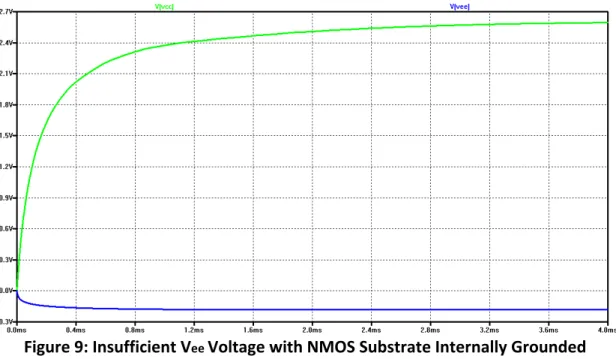
negative voltage with respect to ground. Initially sensor data was output to a CMOS
analog switch, which was used to control an NMOS transistor with an internally
connected substrate placed across the secondary inductor. This resulted in an
asymmetric build up of the supply voltages, as depicted below in Figure 9, where Vcc
was unaffected but the capacitor responsible for Vee was never able to charge due
to the transistor being forced into saturation without a properly connected
Figure 9: Insufficient Vee Voltage with NMOS Substrate Internally Grounded
A bilateral switch was then selected with separate access to substrate and VDD.
Connecting VDD to the positive capacitor and the substrate to the negative capacitor
creates a symmetric circuit and insures equal voltage difference between Vcc and
ground, and ground and Vee, and thus enabling the split supply to provide adequate
voltage for the sensor. The control pin of the switch is connected to the output of
the sensor. The digital data of the sensor toggles the switch, shorting L2 when the
output is high and opening L2 when the output is null. The bidirectional nature of
the switch allows either end of the switch to be connected to either end of the
inductor.
In order to obtain data from the primary coil an envelope detector circuit
must be used. An envelope detector contains a diode, capacitor, and resistor and
envelope frequency. A similar type of Schottky diode will be used and the resistor
and capacitor value will be selected based on the relation:
fc > !
!!"# (6)
where fc is the 15MHz carrier frequency. Either the resistor or the capacitor value
can be selected and the other solved for. A 10pF capacitor was chosen and a 1kΩ
resistor was calculated.
The output of the envelope detector is fed into a low-‐pass filter consisting of
a resistor and a capacitor. The low-‐pass filter acts to remove the 15MHz carrier
frequency leaving only the modulating envelope frequency, which is in the low
kilohertz range. The selection of the resistor and capacitor value is determined by
the relation:
f = !!"#! (7)
where f is the frequency of the data, and R and C are the values of the resistor and
capacitor in ohms and farads respectively. A 10nF capacitor was selected and a 4kΩ
resistor was calculated.
The clean signal from the low-‐pass filter can then be amplified for use with a
microcontroller.
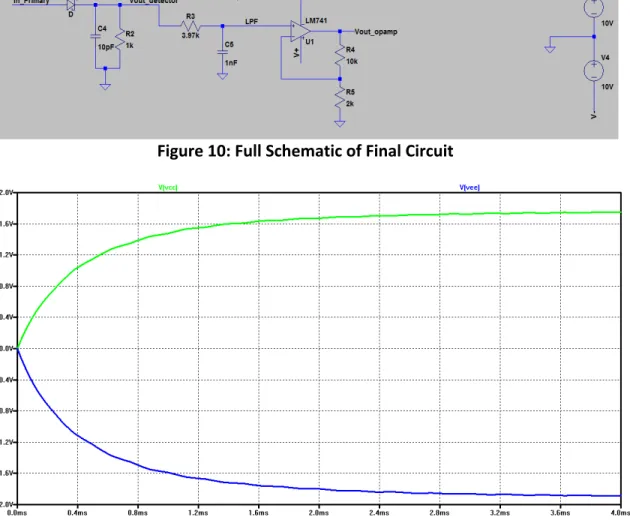
The complete circuit schematic as well as corresponding waveforms from
Figure 10: Full Schematic of Final Circuit
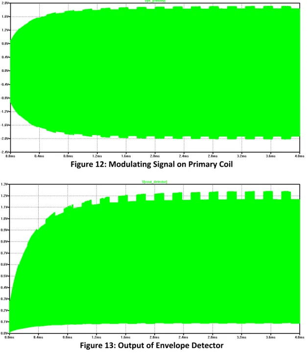
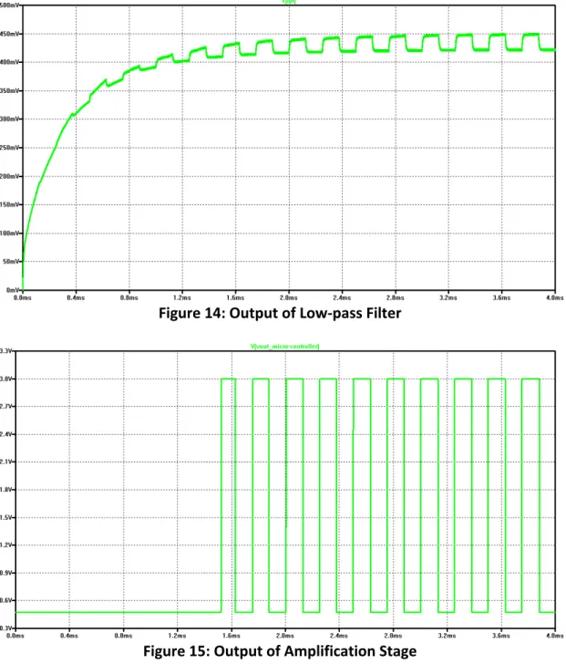
Figure 12: Modulating Signal on Primary Coil
Figure 13: Output of Envelope Detector
Figure 14: Output of Low-‐pass Filter
Figure 15: Output of Amplification Stage
Figure 10 represents the final circuit to be implemented. The buildup of supply
voltage across the split supply rectifier is represented in Figure 11, where symmetry
can now be seen. The different output stages are shown in Figures 12, 13, 14, and
The level of amplification was chosen on the basis of achieving greater than 1V peak,
which most microcontrollers will accept as logic high. The level of amplification can
V. Development and Construction
The first step in the build process was the assembly of the inductors. Initially
a scientific design approach was taken with the use of an inductance calculator. The
inductance calculator, shown in Figure 16, takes into consideration the number of
turns, the magnetic permeability of the core, the wire radius, and the radius of the
core and uses an equation to determine an inductor value.
Figure 16: Screenshot of Inductance Calculator Used
It was discovered that values yielded by the calculator were substantially larger than
the actual measured values after making the inductors. This is explained by the
calculator’s assumption that the relative permeability of the medium is uniform
relative permeability of 2000 – 6000, depending on flux density. Therein lies the
problem, much of the medium is air, which has a relative permeability of
approximately 1. The disparity in the different values heavily skewed the results
produced by the calculator, which was deemed unusable. What followed was
largely an empirical design approach.
Originally the attempt was to make two equal inductors, however, it was
later determined via testing that equal value inductors would not be able to provide
sufficient voltage across the split supply. Inability to meet voltage demands with
equal inductors stems largely from a combination of a poor coupling coefficient, and
more so, turns ratio considerations, which are shown below:
!"!" = !"!" (8)
where Vs is the voltage across the secondary coil, Vp is the voltage across the
primary coil, and Np and Ns are the number of turns across the primary and
secondary coil respectively. By appropriate selection (1:2) of ratio of turns voltage
amplification can occur and sufficient voltage and be provided. For this case Ns must
be greater than Np.
Selecting a capacitor to place in parallel with the primary inductor requires
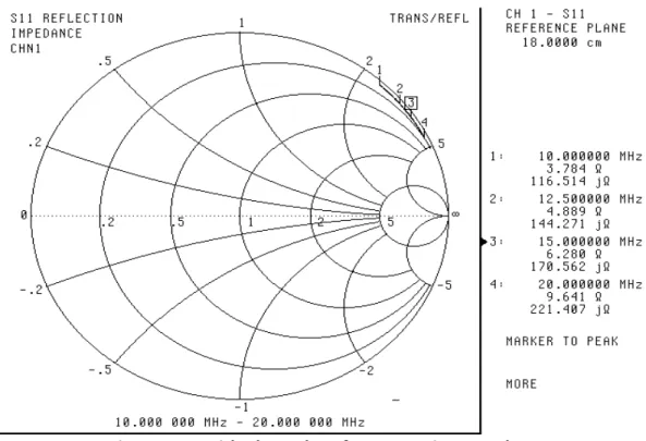
accurate characterization. Inductance measurements were performed using the
Vector Network Analyzer. A Smith Chart was obtained from the Network Analyzer
of the primary coil that yielded optimal performance was measured to be 1.81µH.
The Smith Chart produced by the Network Analyzer is shown in Figure 17.
Figure 17: Smith Chart Plot of 1.81µH Primary Inductor
A capacitor value of 60pF was calculated and used for resonance at 15MHz.
A much larger inductor was used on the secondary side, measuring 6.197µH.
The Network Analyzer produced Smith Chart for the secondary inductor is
Figure 18: Smith Chart Plot of 6.197µH Secondary Inductor
The inductors used in the final circuit are pictured in Figure 19. The pot core height
of the inductors is approximately 3mm.
During the duration of the project it was realized that the particular sensor
purchased would be unable to produce measurable data without first being
interfaced with a microcontroller. Using a microcontroller in the circuit was not
realizable due to the increased power demands brought on by the microcontroller
as well as the coding that would have been necessary for interfacing. The focus of
the project shifted from a designing an actual device to instead a proof of concept
demonstration. The sensor was abandoned and instead a Voltage Controlled
Oscillator (VCO) was utilized to simulate data bits. The split supply was used to
power the VCO and the output of the VCO connected to the control pin of the
bilateral switch across the secondary coil. The VCO output is DC pulses with a
selected frequency of 4kHz, similar to the output of most digital sensors. The VCO
accomplishes shorting and opening of the second coil and the effects can be
VI. Integration and Testing
Testing had been conducted throughout to verify individual components of
the system were functioning properly. Testing of the fully integrated system
involved using an oscilloscope to observe the voltage across the split supply while
noting the voltage required of the function generator, the effect of the switching at
the both the primary and secondary coils, and the waveforms of the various output
stages as they correspond to the output of the VCO. Figure 21 shows a screen
capture of the oscilloscope depicting the signal across the primary coil and the
voltage across the split supply.
Figure 21: Channel 1 (Top) Signal Across Primary Inductor (15Vpp); Channel 2
A 15Vpp AC signal was supplied at a frequency of 15MHz by the Function Generator;
the voltage across the primary coil shows approximately 3.2Vpp, and the voltage
supplied by the split supply shows approximately 4.90V. It is important to note that
the data represents measurements taken from a fully integrated and loaded system.
The envelope detector circuit designed and attached in parallel with the
primary coil functioned according to theory. The output of the envelope detector
showed half-‐wave rectification, though little can be discerned by still screen shots.
The amplitude of the 15MHz signal is shown rectified and modulated, though still
captures yield the 15MHz in an arbitrary state of modulation as opposed to an
outline of a waveform which can be appreciated after the low-‐pass filter stage.
The depth of modulation is to a certain extent determined by the value of
the resistor driving the circuit on the primary side, initially too small of a resistor was
being used to notice significant modulation. The value of the resistor was increased
to approximately 1.0kΩ, where the depth of modulation appeared to be optimized.
The low-‐pass filter produced a visibly modulated signal with the 15MHz
carrier frequency removed. The maxima and minima of the waveform are directly
Figure 22: Channel 1 (Top) Showing the Output of the VCO (3.3Vpp); Channel 2
(Bottom) Showing the Output of Low-‐pass Filter (325mVpp)
As can be seen the frequency of the modulated signal is identical to the frequency of
the VCO.
In order for the data to be interpreted as logic highs and lows the signal out
of the low-‐pass filter must be amplified. A non-‐inverting operational amplifier (part
number LM741) was utilized; a comparator could also have been used. The resistors
of the amplifier were chosen to achieve a signal with greater than 1V peak (10kΩ
and 2kΩ to set Vout = 6Vin), however, this could be further increased if necessary. A
capture of the amplification stage output is shown in Figure 24.
Figure 24: Channel 1 (Top) Showing the Output of the VCO (3.3Vpp); Channel 2
(Bottom) Showing the Output of the Amplification Stage (Vout = 1.95Vpp)
The output of the amplifier should in theory be capable of being used as an input to
a microcontroller; this was beyond the scope of the project mainly due to time
constraints but is an option for future research. The use of a microcontroller would
enable data to be displayed on an LCD screen.
VII. Conclusion and Recommendations
The design implemented in this project is capable with the use of a function
generator of supplying wireless power to a passive DC pulse generator and sensing
its output. The implications of such research are expansive and can be applied to
numerous other fields. One such possible biomedical application would be replacing
the current procedure that diabetic individuals undergo when checking blood insulin
levels. Currently diabetics must puncture their finger to obtain a blood sample for
analysis outside of the body. The possibility of using an implanted sensor and
obtaining data wirelessly is something for consideration using the concepts
presented. Another possible application would be sensing of epileptiform activity.
Research being conducted on individuals suffering from epilepsy involves a
permanent hole in a patient’s skull increasing the patient’s risk of infection as well as
reducing overall protection for the brain. The initial concept of using a tire
pressure sensor would still be a viable option provided a sensor better suited to this
application.
One area of research that would aid advancement would be studying the
effects of different media between the two coils. Having an interface of tire material
between the two coils might have a consequence on the efficiency and practicality
The entire system prototype was constructed on two breadboards which led
to a bulky and fragile circuit. The use of strictly surface mount components on a
printed circuit board would dramatically reduce size and greatly improve reliability.
Furthermore, using a local oscillator as opposed to a function generator would
VII. Bibliography
1. Alexander, Charles K., and Matthew N. O. Sadiku. Fundamentals of Electric
Circuits. Boston: McGraw-‐Hill, 2009.
2. Iskander, Magdy F. Electromagnetic Fields and Waves. Englewood Cliffs, NJ:
Prentice Hall, 1992.
3. Skilling, Hugh Hildreth. Electromechanics: a First Course in Electromechanical
Energy Conversion. Huntington, NY: R.E. Krieger Pub., 1979.
Appendices
A. Parts List and Cost
Part Unit Price ($) Quantity Total Price ($)
Pot Core 0.60 2 1.20
VCO (LTC6069F) 2.48 1 2.69
30-‐Gauge Wire 1.25 1 1.25
5082-‐2835 Schottky Diode 2.05 1 2.05 HSMS-‐2822 Schottky Diode 1.59 1 1.59 CD4016BCN Bilateral Switch 1.29 1 1.29
741 Op Amp 0.35 1 0.35
Assorted Resistors 0.10 9 0.90
Assorted Capacitors 0.50 9 4.50
Table 1: Parts List and Cost
B. Time Allocation Estimates
Task Estimated Time (Hours) Actual Time (Hours)
Research 35 25
Component Selection 5 15
Design 35 30
Construction/Troubleshooting 25 35
Testing 20 25
Report 25 30
Total 145 160
C. Derivation of Operating Principle
Figure 26: An Equivalent T Circuit with an Open Load
Figure 26 shows the lumped circuit equivalent of inductively coupled coils, where L1
is the primary inductor, L2 is the secondary inductor, and M is the mutual
inductance. Applying Kirchhoff’s Voltage Law produces the following equation:
V = I[jω(L1 -‐ M) + jωM]
which simplifies to:
!
! = jωL1 – jωM + jωM
canceling terms and substituting Z = !! yields:
It can be seen that input impedance of the T network when the load is left open is
just the impedance of L1. Therefore:
Lseen = L1
Figure 27: An Equivalent T Circuit with a Short Load
Figure 27 shows the lumped circuit equivalent of inductively coupled coils, where L1
is the primary inductor, L2 is the secondary inductor, and M is the mutual
inductance. The case of the short load represents the case when the switch across
the secondary coil is closed. Applying Kirchhoff’s Voltage Law to solve for the
impedance of the network produces the following equation:
Z = jω(L1 – M) + jω(L2-‐M)||M
Expanding:
Z = jω(L1 – M) + !"!!!!!!!! !!! !!"#!
Adding terms:
Z = ! !!!!!!!!"#!!!!!!!!!!!!!
Expanding the numerator:
Z = !!!!!!!!!"!!"#!!!!!!!!!!!!!!
Simplifying:
Z = !!!!!"#!!!!!!!!
Factoring out ω:
Z = (!!!!"!!!!!)!
Plugging in for M = k !1!2
Z = !(!!!!!"!!!!!!!!)
Factoring the numerator:
Z = !"!!!"!(!!!!!)
Canceling L2 term:
Z = !"!(!!!!!) = -‐jωL1(!!−1) = jωL1(1 − !!)
Z = jωL1(1 − !!)
Therefore, the inductance seen at port 1 when port 2 is shorted is as follows:
Lseen = L1(1 − !!)