COURSE 5
QUANTUM TRANSPORT IN
SEMICONDUCTOR-SUPERCONDUCTOR
MICROJUNCTIONS
C.W.J. Beenakker
Instituut-Lorentz, Umversity of Leiden 2300 RA Leiden, The Netherlands
E Akkermans, G Montambaux, J -L Pichard and J Zinn-Justin, eds Les Hauches, Session LXI, 1994
Physique Quantique Mesoscopique MesoAcopic Quantum Physics
© 1995 Eisevier Science B V All rights reserved
Contents
1 Intioduction 283 2 Scatteimglheoiy 286 3 Thiee simple apphcations 292 3 l Quantum point contact 292 3 2 Quantum dot 293 3 3 Disoidered ]unction 29"5 4 Weak locahzation 297 5 Rcflectionless tunnehng 300 5 l Numencal simulations 300 "5 2 Scalmg theory 303 5 3 Double-bainei junction 308 5 4 Cncuit theoiy 311 6 Universal conductance fluctuaüons 316 7 Shotnoise 318 8 Conclusion 320 Refeiences 322
1. Introduction
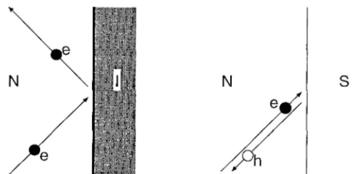
At the Interface between a normal metal and a superconductoi, dissipative eleo tncal current is converted into dissipationless supercurrent The mechamsm foi this conversion was discovered thirty years ago by A F Andreev [1] An elec-tron excitation shghtly above the Fermi level in the normal metal is reflected at the Interface äs a hole excitation shghtly below the Fermi level (see fig 1) The missing Charge of 2e is removed äs a supeicurrent The reflected hole has (ap-proximately) the same momentum äs the mcident electron (The two momenta aie precisely equal at the Fermi level) The velocity of the hole is minus the ve-locity of the electron (cf the notion of a hole äs a "time-ieversed" electron) This cunous scattenng process is known äs retro-reflection or Andreev reflection
The early theoretical work on the conductance of a normal-metal - supercon-ductor (NS) junction treats the dynamics of the quasiparticle excitations semi-classically, äs is appropnate for macroscopic junctions Phase coherence of the electrons and the Andreev-reflected holes is ignored Interest m "mesoscopic" NS junctions, where phase coherence plays an important role, is a recent devel-opment Significant advances have been made dunng the last few years m oui understanding of quantum mterference effects due to phase-coherent Andreev re-flection Much of the motivation has come from the technological advances m the fabncation of a highly transparent contact between a superconductmg film and the two-dimensional electron gas in a semiconductor heterostructure These Systems aie ideal for the study of the mterplay of Andreev reflection and the mesoscopic effects known to occur in semiconductor nanostructures [2], because of the large Fermi wavelength, large mean free path, and because of the possibility to confine the carners electrostatically by means of gate electrodes In this senes of lectures we review the present Status of this rapidly developing field of research
To appreciate the importance of phase coherence m NS junctions, consider the resistance of a normal-metal wire (length L, mean free path l) This resistance increases monotomcally with L Now attach the wire to a superconductor via a tunnel bainer (transmission probabihty Γ) Then the resistance has a mimmum when L ~ l/T The mimmum disappears if the phase coherence between the electrons and holes is destroyed, by mcreasing the voltage or by applymg a mag-r neue field The resistance mmimum is associated with the crossover from a Γ"1
284 C WJ Beenakker
Fig l Normal leflection by an msulator (I) veisus Andreev leflection by a superconducloi (S) of an election excitation in a normal metal (N) neai the Feimi level Normal leflecüon (left) conseives chaige but does not conseive momentum Andieev reflection (nght) conseives momentum but does not conserve chaige The election (c) is reflected äs a hole (h) with the same momentum and opposite vclocity The missmg Charge of 2e is absoibed äs a Cooper pair by the superconducting condcnsate
to a Γ 2 dependence on the barner transparency The Γ 2 dependence is äs ex-pected for tunnehng into a superconductor, being a two-particle piocess The Γ"1 dependence is surpnsmg It is äs if the Andreev-reflected hole can tunnel through the barner without reflections This so called "reflectionless tunnehng" requues telatively transparent NS Interfaces, with Γ > l/L Semiconductor — supercon-ductor junctions are convenient, smce the Schottky barner at the Interface is much more transparent than a typical dielectnc tunnel barner The technological effoit is directed towards making the Interface äs tianspaient äs possible A neaily ideal NS inteiface (Γ ~ 1) is tequired if one wishes to study how Andieev reflection modifies the quantum interference effects m the normal state (Foi Γ <C l these are obscured by the much larger reflectionless-tunnehng effect) The modifica-tions can be quite remarkable We discuss two examples
The first is weak locahzation In the normal state, weak locahzation can not be detected in the current-voltage (I—V) charactenstic, but requires apphcation of a magnetic field The reason is that apphcation of a voltage (in contrast to a mag-netic field) does not break time-reversal symmetry In an NS junction, however, weak locahzation can be detected m the I—V charactenstic, because apphcation of a voltage destroys the phase coherence between electrons and holes The result is a small dip in dl/dV versus V around V = 0 for Γ ~ l On reducing Γ, the dip ciosses over to a peak due to reflectionless tunnehng The peak is much laigei than the dip, but the widths are approximately the same
Quantum Transport m Semiconductor-Superconductor Microjunctions 285
leduces the vanance by precisely a factor of two In an NS junction, the conduct-ance fluctuations are also size and disorder mdependent Howevei, application of a time-reversal-symmetry breakmg magnetic field has no effect on the magnitude These three phenomena, weak locahzation, reflectionless tunneling, and uni-versal conductance fluctuations, are discussed m sections 4, 5, and 6, respectively Sections 2 and 3 are devoted to a descnption of the theoretical method and to a tew illustrative apphcations The method is a scattenng theory, which relates the conductance GNS of the NS junction to the 7V χ 7V transmission matrix i in the noimal state (7V is the number of Iransveise modes at the Ferrm level) In the limit of zero temperature, zero voltage, and zero magnetic field, the relationship is
4e2 Λ Τ2
. " v,. (l 1)
where the transmission eigenvalue Tn is an eigenvalue of the matnx product iit
The same numbers Tn (n = l, 2, , 7V) determme the conductance GN in the
normal state, accordmg to the Landauer formula
The fact that the same transmission eigenvalues determme both GN and GNS means that one can use the same (numencal and analytical) techniques developed for quantum transport in the normal state This is a substantial technical and conceptual simplification
The scattenng theory can also be used foi other transpoit properties, other than the conductance, both in the normal and the superconducting state An example, discussed in section 7, is the shot noise due to the discreteness of the camers A doubling of the ratio of shot-noise power to current can occur in an NS junction, consistent with the notion of Cooper pair transport m the superconductor
We conclude in section 8
relation-286 C WJ Beenakker
ship in terms of the transmission eigenvalues Tn in the normal state We do not
discuss the Josephson effect here, but refer to ref [8] for a review of mesoscopic SNS junctions Taken together, ref [8] and the present work descnbe a unified approach to mesoscopic superconductivity
2. Scattering theory
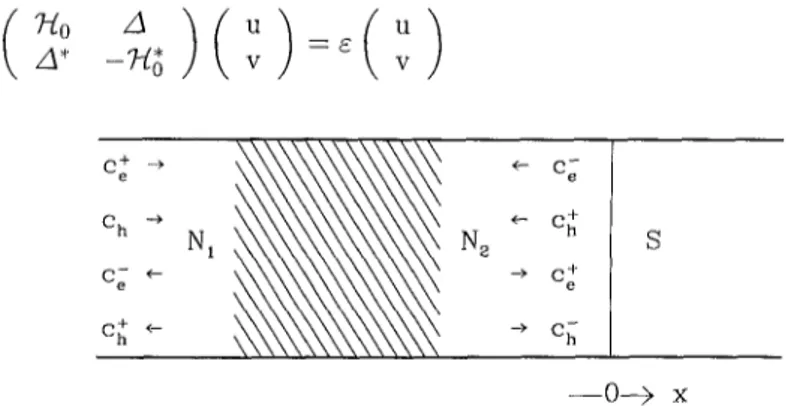
The model considered is illustrated in fig 2 It consists of a disordered normal re-gion (hatched) adjacent to a superconductor (S) The disordered rere-gion may also contain a geometncal constnction or a tunnel barner To obtain a well-defined scattenng problem we insert ideal (impunty-free) normal leads NI and N2 to the left and nght of the disordered region The NS Interface is located at χ = 0 We assume that the only scattenng in the superconductor consists of Andreev reflec-tion at the NS mterface, i e we consider the case that the disorder is contamed entirely within the normal region The spatial Separation of Andreev and noimal scattenng is the key simplification which allows us to relate the conductance dir-ectly to the normal-state scattenng matnx The model is dirdir-ectly applicable to a superconductor in the clean limit (mean free path in S large compared to the superconducting coherence length ξ), or to a pomt-contact junction (formed by a constnction which is narrow compared to ξ) In both cases the contribution of scattenng within the superconductor to the junction resistance can be neglected [9]
The scattenng states at energy ε are eigenfunctions of the Bogoliubov-de Gennes (BdG) equation This equation has the form of two Schrodmgei equa-tions for electron and hole wavefuncequa-tions u(r) and v(r), coupled by the pan Potential A(r) [10]
Δ
A" ( 2 l )
0— > χ
Quantum Transport m Semiconductor-Superconductor Microjmctwns 287
Here Tio = (p + eA)2/2m + V — Εγ is the single-electron Hamiltoman,
con-taining an electrostatic potential V (r) and vector potential A(r) The excitation eneigy ε is measured relative to the Fermi energy Ep To simphfy construction of the scattenng basis we assume that the magnetic field B (in the z-direction) vanishes outside the disordered region One can then choose a gauge such that A Ξ 0 m lead N2 and in S, while AX,AZ = 0, Ay = AI = constant m lead NI
The pair potential m the bulk of the superconductor (χ ^> ζ) has amphtude Δ0
and phase φ The spatial dependence of Δ(Γ) near the NS Interface is determmed by the self-consistency relation [10]
^(r) = |5(r)| ^v*(r)u(r)[l-2/(e)], (22)
ε>0
wheie the sum is over all states with positive eigenvalue, and /(ε) = [l + exp(s/k^T)}'~1 is the Fermi function The coefficient g is the mteiaction
con-stant of the BCS theory of superconductivity At an NS mteiface, g diops abruptly (over atomic distances) to zero, in the assumed absence of any painng interaction m the normal region Therefore, Δ(τ) = 0 for χ < 0 At the superconductmg side of the NS Interface, A(r) recovers its bulk value A0e"* only at some distance from the Interface We will neglect the suppression of A(r) on approaching the NS mterface, and use the step-function model
A(r) = Δ0Βιφθ(χ) (2 3)
This model is also refeired to m the literature äs a "rigid boundary-condition" Likhaiev [11] discusses m detail the conditions foi its validity If the width W of the NS junction is small compared to ξ, the non-umfoimities in Δ(τ) extend only over a distance of order W fiom the junction (because of "geometucal dilu-tion" of the influence of the nanow junction in the wide superconductor) Since non-umfoimities on length scales <C ξ do not affect the dynamics of the qua-siparticles, these can be neglected and the step-function model holds A pomt contact 01 microbndge belongs m geneial to this class of junctions Alternat-ively, the step-function model holds also foi a wide junction if the lesistivity of the junction region is much bigger than the resisüvity of the bulk superconductor This condition is formulated more precisely in ref [11] A semiconductor — su-perconductor junction is typically in this second category Note that both the two cases are consistent with our assumption that the disorder is contamed entirely within the normal region
288 C WJ Beenakker
by
$(r) = £V(r)u(r)[l-2/(e)] (2 4)
ε>0
Phase coherence between the electron and hole wave functions u and v leads to Φ(τ-) φ 0 for χ < 0 The term "proximity effect" can therefore mean two differ-ent thmgs One is the suppression of the pair potdiffer-ential Δ at the superconducting side of the NS mterface This is a small effect which is neglected in the piesent work (and m most other papers in this field) The other is the induction of a non-zeio order parameter Φ at the normal side of the NS mterface This effect is fully mcluded here, even though Φ does not appear exphcitly m the expiessions which follow The reason is that the order parametei quantifies the degree of phase co-heience between electrons and holes, but does not itself affect the dynamics ot the quasiparticles (The BdG equation (21) contams Δ not Φ )
We now construct a basis for the scattenng matnx (s matnx) In the noimal lead N2 the eigenfunctions of the BdG equation (2 1) can be wntten m the form
ο
ι )(Ο~1 / 2Φη(2/,*)βχρ(±<τ), (25)
wheie the wavenumbers k^ and fcjj are given by
^ = (2m/ri2)1/2(£F - En + σ* he)l'\ (2 6)
and we have defined ae Ξ l, ah = — l The labels e and h mdicate the election
or hole character of the wavefunction The mdex n labels the modes, Φ „,(?/, ζ) is the transverse wavefunction of the n-th mode, and En its threshold energy
[(pl + pl}/2m + V(y, z}}$>n(y, z) = En$n(y, z) (2 7)
The eigenfunction Φη is normahzed to unity, Jdy/dz^7 l|2 = l With this
normahzation each wavefunction in the basis (2 5) carnes the same amount of quasiparticle current The eigenfunctions in lead NI are chosen similarly, but with an additional phase factor exp[—:σ6 h( e A i / f i ) y ] from the vector potential
A wave incident on the disordered normal region is descnbed m the basis (2 5) by a vector of coefficients
φ" Ξ (c+(N1),C-(N2),C l7(N1))c+(N2)) (28)
(The mode-mdex n has been suppressed for simphcity of notation ) The leflected and tiansmitted wave has vector of coefficients
Quantum Transport in Semiconductor—Superconductor Micro]unctions 289
The 5-matrix SN of the normal region relates these two vectois,
CN = SN CN (2 10)
Because the normal region does not couple electrons and holes, this matrix has the block-diagonal form
;ο(ε) Ο 0 s0(-e)*
Heie SQ is the unitary s-matrix associated with the single-electron Hamiltoman ΉΟ The leflection and transmission matnces r(e) and t (ε) are N χ Ν matnces, N (ε) being the numbei of propagatmg modes at energy ε (We assume foi sim-plicity that the numbei of modes m leads NI and N2 is the same ) The matnx SQ is unitaiy (S'QSO = 1) and satisfies the symmetry lelaüon So(e, _B)tJ = So(e, —B)^
ForeneigiesO < ε < Δ0 there are no propagatmg modes m the supeiconductor
We can then define an s-matnx foi Andreev leflection at the NS Interface which iclates the vector of coefficients (c~(N2),c,|(N2)) to (c+(N2),c,7(N2)) The elements of this s-matrix can be obtamed by matching the wavefunctions (2 5) at χ = 0 to the decaymg solutions in S of the BdG equation If teims of oidei ΔΟ/ΕΓ aie neglected (the so called Andreev approximation [1]), the lesult is
simply
ο+(Ν2)=αβ-ι ψοε+(Ν2), (212)
where α Ξ exp[—iaiccos(e/Zi0)] Andreev reflection tiansfoims an election mode mto a hole mode, without change of mode mdex The transformation is accompamed by a phase shift, which consists of two paits
(i) A phase shift — arccos(s/Zi0) due to the penetration ot the wavefunction mto the superconductor
(n) A phase shift equal to plus or minus the phase of the pair potential in the supeiconductoi (plus for leflection fiom hole to election, minus foi the reverse process)
We can combine the 27V linear lelations (2 12) with the 47V relations (2 10) to obtain a set of 27V" linear relations between the incident wave in lead NI and the leflected wave in the same lead
4(Νι) = ^(NO + S^NO (2 13)
The four N χ N matnces see, Shh» seh» ar|d siie form togethei the scatteung matnx s of the whole System for energies 0 < ε < Δ0 An electron incident in
290 C WJ Beenakker
hole (with scattenng amphtudes She) Similarly, the matnces s^ and seh contain
the scattenng amphtudes for reflection of a hole äs a hole or äs an electron After some algebra we find for these matnces the expressions
5ββ(ε) = Γ11(ε) + α2ί12(ε)Γ*2(-ε)Μ6ί21(ε), (2 14)
sM=ril(-e) + <*>tu(-e)r22(e)Mht*21(-e), (215)
seh(e) = ae1*i1 2(e)Afhi21(-e), (2 16)
she(e) = ae-'%*2(-e)Mei21(e), (2 17)
where we have defined the matnces
Mh = [l - a2r2*2(-e)r22(£)]-1 (2 18)
One can venfy that the s-matnx constructed from these four sub-matrices satisfies umtanty (s^s = 1) and the symmetry relation s(e, B, φ\3 = s(e, —B, —φ)^, äs
required by quasiparticle-current conservation and by time-reversal invanance, respectively
Foi the hnear-response conductance GNS of the NS junction at zero temperature we only need the s-matrix at the Fermi level, i e at ε = 0 We restnct ourselves to this case and omit the argument ε in what follows We apply the general formula [12-14]
GNS = ^Tr (l - See4 + S h e Stj = ^!Tr S h e Ste (2 19)
The second equahty follows from unitarity of s, which imphes l — seeSee =
sehslh = (sD'^he^he^e. so that Tr (l ~ See4) = Tr sh esje We now substi-tute eq (2 17) ior ε = 0 (a = -i) mto eq (2 19), and obtam the expression
GNS = ^-Tr42i12(l +r2y22)-1i2<1iJ1(l + r^)-1 , (220)
where MT = (M*) t denotes the transpose of a matnx The advantage of eq (2 20) over eq (2 19) is that the former can be evaluated by usmg Standard tech-niques developed for quantum transport m the normal state, since the only mput is the normal-state scattenng matrix The effects of multiple Andieev leflections aie fully mcorporated by the two matrix inversions in eq (2 20)
In the absence of a magnetic field the general formula (2 20) simplifies consid-erably Since the s-matrix SQ of the normal region is Symmetrie foi B = 0, one has r22 = r%2 and i12 = iJi Equation (2 20) then takes the form
Quantum Transport in Semiconductor-Superconductor Microjunctions 291
(221)
In the second equahty we have used the unitanty relation r2 2r2 2 + ί|2ί12 = l The trace (221) depends only on the eigen values of the Hermitian matnx tl2tl2 We denote these eigenvalues by Tn (n = l, 2, 7V) Since the matnces
ti2tl2, ^i2ii2, 4i*2i' anc' *2i4i aU nave the same set of eigenvalues, we can omit the indices and wnte simply ttf We obtain the followmg relation between the conductance and the transmission eigenvalues
4e2 J^ T2
<*·· = -*- Σ erf·? S2Z)
This is the central icsult of ref [15]
Equation (2 22) holds for an arbitrary transmission matnx t, i e for arbitrary disordei potential It is the multi-channel generalization of a formula first obtamed by Blonder, Tmkham, and Klapwijk [12] (and subsequently by Shelankov [16] and by Zaitsev [17]) for the smgle channel case (appropnate for a geometiy such äs a planar tunnel barner, where the different scattermg channels are uncoupled) A formula of similar generahty for the normal-metal conductance G N is the multi-channel Landauer formula
_ T n (223)
n=l
In contrast to the Landauer lormula, eq (2 22) for the conductance of an NS junction is a non linear function of the transmission eigenvalues Tn When deal-ing with a non-hnear multi channel formula äs eq (2 22), it is of importance to distinguish between the tiansmission eigenvalue Tn and the modal transmission piobability Tn = X)m_1 \tnm 2 The former is an eigenvalue of the matnx ift, the latter a diagonal element of that matnx The Landauer formula (2 23) can be written equivalently äs a sum over eigenvalues or äs sum over modal transmission probabihties
η Ξ τ η (224)
n=l n=l
one-292 C WJ Beenakker
dimensional Blonder-Tinkham-Klapwijk foimula to more dimensions by sum-mmg over modal tiansmission probabilities (or, equivalently, by angulai avei-agmg) were not successful precisely because only the diagonal elements of ttf weie considered
3. Three simple applications
To illustrate the power and generahty of the scattenng formula (2 22), we discuss in this section three simple applications to the ballistic, resonant-tunneling, and diffusive transport regimes [15]
3 l Quantum point contact
Consider first the case that the normal metal consists of a ballistic constnction with a normal-state conductance quantized at GN = 27V"oe2 /h (a quantum point
contact) The integei NO is the numbei of occupied one-dimensional subbands
(per spm direction) in the constnction, or alternatively the numbei of Iransveise modes at the Fermi level which can propagate through the constnction Note that TVo -C N An "ideal" quantum point contact is charactenzed by a special set of transmission eigenvalues, which are equal to either zero 01 one [2]
l if l < n < 7 V0 > n n
0 if 7V0 <n<N, ( '
wheie the eigenvalues have been ordered from large to small We emphasize that eq ( 3 1 ) does not imply that the transport through the constnction is adiabatic In the case of adiabatic transport, the transmission eigenvalue Tn is equal to the modal transmission probability Tn In the absence of adiabaticity there is no direct lelation between Tn and Tn Substitution of eq (3 1) mto eq (2 22) yields
GNS = ^-No (3 2)
h
The conductance of the NS junction is quantized in units of 4e2//i This is twice the conductance quantum in the normal state, due to the current-doubling effect of Andreev reflection [18]
Quantum Transport m Semiconductor-Superconductor Micmjunctions 293
0)
N
0
2
4
6
(E
F-V
0)/h
WxFig 3 Solid curve Conductance GNS veisus Feimi energy of a quanlum pomt contact between a noimal and a supeiconductmg teseivoir (shown schematically m the inset) The dotted cuive is twice the conductance GN forthe case of two noimal reservons [20] The constuction is defined by the 2D saddle pomt potential V(x y) = V0 — |m with ων/ωχ = 3
fiom eq (2 22) with Tn = [l + εχρ(~2πεη/1ΐωχ)] J e„ Ξ £r - VQ - (n - \]
lef [15])
is calculated ίϊω,, (Fiom
tiansition icgion, where GNS lies below twice GN This is actually a ngoious
inequality, which follows from eqs (2 22) and (2 23) foi arbitrary transmission matnx
5·· 2GN, V i (33)
3 2 Quantum dot
Consider next a small confined region (of dimensions comparable to the Fermi wavelength), which is weakly coupled by tunnel barners to two electron lesei voirs We assume that transport through this quantum dot occurs via resonant tunnehng thiough a smgle bound state Let £res be the energy of the resonant
294 C.W.J. Beenakker
ω
•Φ
ü
0
N
-5
l l Γ
i/1 BW
0
e
res/7
Fig. 4. Conductance versus energy of the resonant level, from eq. (3.8) for the case of equal lunnel barriers (solid curve). The dotted curvc is the Breit-Wigner transmission probability (3.4). The inset shows schematically the normal-metal — quantum-dot — superconductor junction.
non-interacting electrons has the form
h n 7i 72 _ ™
TT^^N — -^ T~i ö = JB W i (3.4)
with TBw the Breit-Wigner transmission probability at the Fermi level. The normal-state transmission matrix £12 (ε) which yields this conductance has matrix elements [21]
r(e)nm =
ε - eres + 517
(3.5)
where Χ)η7ιη Ξ 7ι> X)n72n = 7z. and Ui, U? are two unitary matrices (which need not be further specified).
Let us now investigate how the conductance (3.4) is modified if one of the two reservoirs is in the superconducting state. The transmission matrix product t12t12
(evaluated at the Fermi level ε = 0) following from eq. (3.5) is
Quantum Transport m Semiconductor-Superconductor Microjunctwns 295
Its eigenvalues are
TBW if n = l,
0 if 2 < n < 7 V (0 ''
Substitution mto eq (2 22) yields the conductance
4e2 / TBW \2 4β2 / 2ΎιΎ2
The conductance on lesonance (eies = 0) is maximal in the case of equal tunnel rates (71 = 72), and is then equal to 4e2//i — independent of 7 The lineshape for this case is shown in fig 4 (solid curve) It differs substantially from the Loientzian lineshape (3 4) of the Breit- Wigner formula (dotted curve)
The amphtude and lineshape of the conductance lesonance (3 8) does not de-pend on the relative magnitude of the resonance width 7 and the superconductmg energy gap Δ0 This is in contrast to the supercurient resonance in a
supercon-ductor — quantum dot — superconsupercon-ductor Josephson junction, which depends sensitively on the ratio Ύ/Δ0 [22,23] The difference can be traced to the fact that
the conductance (m the zero-temperatuie, zeio-voltage hmit) is stnctly a Fermi-level propeity, whereas all states withm Δ0 of the Fermi level contnbute to the
Josephson effect (For an extension of eq (3 8) to finite voltages, see ref [24] ) Smce we have assumed non-mteracting quasiparticles, the above results apply to a quantum dot with a small chargmg energy U foi double occupancy of the les-onant state Devyatov and Kupnyanov [25], and Hekking et al [26], have studied the influence of Coulomb repulsion on lesonant tunnelmg through an NS junction, m the temperature regime kßT ^> 7 where the resonance is thermally broadened The extension to the low-temperatuie regime of an intnnsically bioadened reson-ance lemains to be investigated
3 3 Disordered junction
We now turn to the regime of diffusive tiansport through a disordered pomt con-tact or microbndge between a normal and a superconductmg leseivoir The model consideied is that of an NS junction contammg a disordered normal legion of length L much greater than the mean free path l for elastic impunty scattenng, but much smaller than the localization length Nl We calculate the average con-ductance of the junction, averaged over an ensemble of impunty configurations We begm by parametenzing the transmission eigenvalue Tn in terms of a channel-dependent localization length ζη
296 C WJ Beenakker
A fundamental result in quantum transport is that the inverse localization length is umformly distnbuted between 0 and 1/Cmm — l/' for / <C L <C Nl [27-30] One can therefore wnte
Λ / V
_1 Π - ί τ , Μ /'"' s"""rlo· f tnna^~~^ <r\ Γ°°
-1
dx f(cosh τ),
0
(310)
where { ) indicates the ensemble aveiage and f (T) is an arbitrary function of the transmission eigenvalue such that f(T) —·> 0 for T -^ 0 In the second equality m eq (3 10) we have used that L/£mm ~ L/l > l to replace the upper Integration limit by oo
Combinmg eqs (2 22), (2 23), and (3 10), we find
cosh~2 χ
<GNS) = 2(GN) / dx —5- = <GN) (3 11)
Jo \ 2 - c o s h xj
We conclude that — although GNS according to eq (2 22) is of second order in the transmission eigenvalues Tn — the ensemble aveiage (GNS) is of first
oider in l/L The resolution of this paradox is that the T's aie not distnbuted umformly, but are either exponentially small (closed channels) 01 of order unity (open channels) [28] Hence the average of T,2 is of the same ordei äs the av-erage of Tn Off-diagonal elements of the transmission matnx ttf are crucial to arnve at the result (311) Indeed, if one would evaluate eq - (2 22) with the tians-mission eigenvalues Tn leplaced by the modal transmission probabihties Tn, one would find a totally wrong result Since Tn ~ l/L <C l, one would find GNS — (//L)GN — which underestimates the conductance of the NS junction by the factor L /l
Previous work [31,32] had obtamed the equality of GNS and GN fiom semi-classical equations of motion, äs was appropnate for macroscopic Systems which are large compared to the normal-metal phase-coherence length Ιψ The piesent denvation, m contrast, is fully quantum mechamcal It apphes to the "meso-scopic" legime L < Ιψ, in which transport is phase coherent Takane and Ebisawa [33] have studied the conductance of a disoidered phase-coherent NS junction by numencal Simulation of a two-dimensional tight-bmding model They found (GNS) = (GN) within numencal accuracy foi / <C L <^i Nl, in agreement with eq (311)
Quantum Transport in Semiconductor—Superconductor Micrnjunctions 297
4. Weak localization
An NSjunction shows an enhanced weak-locahzation effect, m companson with the noimal state [15] The oiigin oi the enhancement can be undeistood in a simple way, äs follows
We ictuin to the parametenzation Tn Ξ l / cosh2 (L / 'ζη) introduced in eq
(3 9), and define the density ot localization lengths ρ(ζ, L) = (Ση ^(C ~~ C?I))L
The subscnpt L icfers to the length of the disordered region Usmg the identity cosh 2x = 2 cosh2 χ — l, the ensemble-average of eq (2 22) becomes
Λ 2 ι oo
(GNS)L = -— dCp(C,£)cosrT2(2L/C) (41) ft Ja
In the same parametenzation, one has
(42) " Jo
In the "open-channel approximation" [34], the Integrals over ζ" aie restncted to the lange ζ > L of localization lengths gieater than the length of the conductoi In this ränge the density ρ(ζ, L) is approximately independent of L The whole L-dependence of the integrands in eqs (4 1) and (4 2) lies then in the aigument of the hypeibohc cosme, so that
<GNS)L = 2<GN)2 L (43)
This denvation formahzes the intuitive notion that Andieev leflection at an NS inteiface etfectively doubles the length of the normal-metal conductoi [33]
Considei now the geometiy W <C L relevant foi a microbndge In the noimal state one has
d e - $ GN ) (44)
wheie CTrjmde is the classical Drude conductivity The L-mdependent term 6G·^ is the weak-locahzation coirection, given by [35] 6G^ = | e2 /h Equation (4 3)
then implies that
<GNS> = (W/L)<7t>lude - 6Gm, (4 5)
with (5GNS = 2(5GN We conclude that Andieev leflection mcreases the weak-locahzation conection, by a factoi of two according to this qualitative argument [15] Angoious theoiy [36-38] of weak localization m a n N S microbndge shows that the mciease is actually somewhat less than a factor of two,*
6GN$ = (2 - 8π"~2) e2/h = l 78 SGN (4 6)
* Equation (46) follows üom the geneial formula SA = |i(l) + J0°°d'c(4x2 + 7r2)- 1a(cosh~2 τ) for the weak localization conection m a wne geometiy wheio A is an aibit
298 C WJ Beenakker
As pointed out m icf [39], the enhancement of weak locahzation in an NS junction can be observed expenmentally äs a dip in the differential conductance G^s(V) = dl/dV around zero voltage The dip occurs because an applied voltage destroys the enhancement of weak locahzation by Andreev reflection, thereby increasmg the conductance by an amount
<5GNS - 6GN « 0 5 e2/h (4 7)
at zero temperature [At finite temperatures, we expect a reduction of the size of dip by a factor* (LC/L)2, where Lc — mm (Ιφ, ^FiD/k^T) is the length over which electrons and holes remain phase coherent ] We emphasize that m the noimal state, weak locahzation can not be detected in the current-voltage charactenstic The reason why a dip occurs in GNS(^) and not m G^(V) is that an applied voltage (m contrast to a magnetic field) does not break time-reversal symmetry — but only affects the phase coherence between the elections and the Andieev-reflected holes (which differ m energy by up to 2eV) The width Vc
of the conductance dip is of the ordei of the Thouless energy Ec = nhD/L2
(with D the diffusion coefficient of the junction, L should be replaced by Lc ή
L > Lc) This energy scale is such that an electron and a hole acquire a phase
difference of order π on traversmg the junction The energy Ec is much smaller
than the superconductmg energy gap Δ0, provided L > ξ (with ξ ~ (/LD/Z\0)1//2 the superconductmg coherence length in the dirty-metal limit) The Separation of energy scales is important, m order to be able to distmguish expenmentally the cunent due to Andreev reflection below the energy gap from the quasi-particle current above the energy gap
The first measuiement of the conductance dip predicted in ref [39] has been leported recently by Lenssen et al [40] The System studied consists of the two-dimensional electron gas in a GaAs/AlGaAs heterostructure with Sn/Ti supei-conducting contacts (W = 10/im, L = 0 8/zm) No supercurrent is observed, presumably because Ιφ ~ 0 4 /im is smaller than L (The phase-coheience length Ιφ is estimated from a conventional weak-locahzation measurement in a mag-netic field ) The data for the differential conductance is reproduced m fig 5 At the lowest temperatures (10 mK) a rathei small and narrow conductance dip develops, supenmposed on a large and broad conductance minimum The size of the conductance dip is about 2e2//i Since in the expenmental geometiy
W > L > Ιφ, and there are two NS Interfaces, we would expect a dip of
or-* The reduction factor (LC/L)2 for the size of the conductance dip when W < Lc < L κ esümated
äs follows Consider the wire äs consistmg of L/LC phase-coheient Segments of length Lc m senes The fiist segment, adjacent to the supeiconductor, has a conductance dip 5G\ ~ e2/ h , while the
othcr Segments have no conductance dip The resistance AI of a smgle segment is a ftacüon LC/L ofthetotaliesistanceßof thewiie Since &G/G = -6R/R = -5Ri/Rima6Ri = -Ä2c5Gi ~
Quantum Transport in Semiconductor-Superconductor Microjunctions
1421—
299
140
138
Π6
134
132
l 05 Ο 05 l 1 5
V (mV)
Fig 5 Diffeiential conductance äs a function of apphed voltage at thiee diffeient tempeiatuies Expei imental data by Lenssen et al foi a two dimensional elcction gas with supeiconducting contacts The dip aiound zeio voltage which is supeiimposed on the broad mmimum at the lowest tempeiatuie is attnbuted to the enhancement of weak locahzation by Andieev reflection (Fiom lef [40])
der 2(W/l</,)(l(f,/L)'2 χ 0 5e2/h ~ 6e2/h, simply by countmg the numbei of
phase coherent Segments adjacent to the superconductor This is thiee times äs laige äs obseived, but the presence of a tunnel barner at the NS Interface might easily account foi this discrepancy (The Schottky barner at the Interface between a semiconductor and superconductor presents a natural ongm for such a barner) The conductance dip has width Vc ~ 0 25 mV, which is less than the energy gap Δ0 = 0 56 meV of bulk Sn — but not by much Experiments with a larger
sep-aiation of energy scales are lequired foi a completely unambiguous Identification of the phenomenon
An essential requirement for the appearance of a dip m the differential con-ductance is a high piobability for Andreev reflection at the NS boundary This is illustrated in fig 6, which shows the results of numencal simulations [39] of ttansport through a disordered normal region connected via a tunnel barner to a superconductor The tunnel barner is chaiactenzed by a transmission probabihty per mode Γ The dash dotted lines refer to an ideal Interface (Γ = 1), and show the conductance dip due to weak locahzation, discussed above For Γ ~ 0 2-0 4 the data for GNS (filled circles) shows a crossover* to a conductance peak This is the phenomenon of reflectionless tunnehng, discussed in the following section
300 C WJ Beenakker
<ΰ ο
Β=0 >-«,
(-ο -·'-*·.-.-.-.-_-.·
>oo o o o·
eV=0
, -β- -ο- - -
-.«---.-2 4 6 0
eV (Ec)
2 4 6
flux (h/e)
Fig 6 Voltage and magnetic field dependence of GNS (filled circles) and GN (open cncles) Nu-mciical Simulation of a disoidered noimal region (L/W = 48, l/L = 0 12, yV = M) in seiies with a tunnel baiuei (tiansmission probability pei mode Γ, dotted lines Γ = 0 2, dashed Γ = 0 6, dash-dotted Γ = 1) Note the crossovei fiom a dip (weak locahzation) to a peak (leflecüonless tunneling) in GNS on teducing Γ (Fiom ref [39] )
5. Reflectionless tunneling
In 1991, Kastalsky et al. [41] discovered a large and nairow peak in the differ-ential conductance of a Nb-InGaAs junction. We reproduce then data in fig. 7. (A similar peak is observed äs a function of magnetic field.) Since then a gieat deal of expenmental [42-48], numencal [39,49], and analytical work [50-54] has been done on this effect. Here we focus on the explanation in terms of disorder-induced openmg of tunneling channels [30,54], which is the most natuial from the view point of the scattenng formula (2 22), and which we feel captuies the essence of the effect. Equivalently, the conductance peak can be explamed m terms of a non-equilibnum proximity effect, which is the preferred explanation in a Green's function formulation of the problem [52,55-57]. We begm by reviewmg the numencal work [39].
5. l. Numencal simulations
Quantum Transport m Semiconductor-Superconductor Microjunctions 301
K
~2
Fig 7 Diffeienüal conductancc (normahzed by the normal-state lesistance AN = 0 27 Ω) äs a function of applicd voltage at seven diffeient tempeiatuies Expeiimental data by Kastalsky et al toi a Nb-InGaAs |unction Note the diffeience with fig 5 A peak rather than a dip develops at the lowest temperatures and the size of the peak (0 6 Ω"1 ~ l 5 χ ΙΟ4 e2/h) is ioui ordeis of magnitude gieatei
iei [4l])
The width of the peak is compaiable to the width of the dip in hg 5 (Fiom
and V in this ränge (open circles), GNS drops abruptly (filled cncles) The width of the conductance peak in B and eV is respectively of order Bc = h/eLW (one flux quantum through the normal legion) and eVc = nhD/L2 = Ec (the Thou-less energy) The width of the peak is the same äs the width of the conductance dip due to weak locahzation, which occurs for larger barnei tianspaiencies The size of the peak is much greater than the dip, however
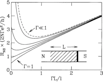
It is mstiuctive to first discuss the classical resistance R^ss of the NS junc-tion The basic approximajunc-tion m R^gss is that cuirents rather than amphtudes aie matched at the NS mterface [31] The result is
P$f = (h/2Ne2) [L/l + 2Γ-2 + 0(1)] (5 1) The contnbution fiom the barner is ex Γ~2 because tunnelmg mto a supeicon-ductor is a two-particle process [58] Both the incident electron and the Andieev-icflected hole have to tunnel thiough the barnei (the net result being the addition of a Cooper pair to the supetconductmg condensate [1]) Equation (5 1) is to be contiasted with the classical resistance R^ass m the noimal state,
R^ = (h/2Ne2) [L/l + Γ'1 + 0(1)] , wheie the contnbution of a icsistive barrier is ex Γ"1
(5 2)
302 C WJ Beenakker
o <J
2
W(u 1 R
\
l ü
£
v
~"
1
K
0 5
n
" ' 1 ' 1 ' 1 '
1 ( a ) J
t
)li
.1 '» 5u p» O,Jl·1 1 1 1 1 1 1 1
> '· 1 ' 1 ' 1 ' 1 '
(b) _
φ
;j * D Π '~ ·
0 l~
4l
~Vits._^:
1 1 1 1 1 1 1 1 1
Γ Γ
Fig 8 Fillecl circles Numencally calculated resistance ANS of a disordered NS ]unction versus Ihe Uansmission probabüity per mode Γ of the tunnel barner at the NS mterface Open ciicles Resistance AN of the same junction in the normal state (a) is for zero magnetic field (b) is foi a flux of 10 h/e
through the disordered legion The dotted and solid curves are the classical eqs (5 1) and (5 2) The dashed cuive is the theory of jef [52] which for Γ 2> l/L fü 0 12 comcides with eq (5 3) (Fiom
lef [39] )
barner (i e for Γ = 1), -RN'gss = R^ss for i » l, in agreement with refs [31,32]
Let us now see how these classical results compare with the simulations [39] In fig 8 we show the resistance (at V — 0) äs a function of Γ in the absence and presence of a magnetic field (The parameteis of the disordered region are the same äs for fig 6 ) There is good agreement with the classical eqs (51) and (5 2) for a magnetic field corresponding to 10 flux quanta through the disordered segment (fig 8b) For 5 = 0, however, the Situation is different (fig 8a) The normal-state resistance (open circles) still follows approximately the classical for-mula (solid curve) (Deviations due to weak locahzation are noticeable, but small on the scale of the figure) In contrast, the resistance of the NS junction (filled circles) lies much below the classical prediction (dotted curve) The numencal data shows that for Γ > l/L one has approximately
Rm (B = 0, V = 0) w J?Nass> (5 3)
which for Γ <c l is much smaller than R^gss This is the phenomenon of
Quantum Transport in Semiconductor—Superconductor Microjunctions 303
et al [50] The numencal data of fig 8a is in good agreement with the Green's function calculation of Volkov, Zartsev, and Klapwijk [52] (dashed curve) Both these papers have played a crucial role in the understandmg of the effect The scal-mg theory reviewed below [54] is essentially equivalent to the Green's function calculation, but has the advantage of explicitly demonstratmg how the opening of tunnelmg channels on increasmg the length L of the disordered region mduces a transition from a Γ~2 dependence to a Γ"1 dependence when L ~ l/T
5 2 Scahng theory
We use the parametenzation
Tn = * , (54)
cosn xn
similar to eq (3 9), but now with a dimensionless variable xn e [0, oo) The
density of the x-variables, for a length L of disordered region, is denoted by
~f rr T\ / V ^ Α Γ τ > rr \\ r (Z. <\
P\<L·, i-i} — \Z-m \ -Ln)/ L \3 3)
Foi L = 0, i e m the absence of disorder, we have the initial condition imposed by the barrier,
p ( x , Q ) = N6(x - x0], (56)
with Γ = l/cosh2xo The scahng theory descnbes how p(x,L) evolves with
increasmg L This evolution is governed by the equation
"r\ 1 A r\ Γ '"•^
— p(x, s) = ττ^~ρ(%, s)—— l dx'p(x',s)ln smh2 x — smh2 x'
os 27V ox ox J0
(57)
where we have defined s = L/l This non-lmear diffusion equation was denved by Mello and Pichard [59] fiom a Fokker-Planck equation [34,60,61] for the jomt distnbution function of all 7V eigenvalues, by integratmg out 7V — l eigenvalues and taking the large-7V limit This limit lestricts its validity to the metallic re-gime (7V ^> L/l), and is sufficient to determme the leading order contribution to the aveiage conductance, which is O (N) The weak-locahzation correction, which is 0(1), is neglected here A priori, eq (5 7) holds only for a "quasi-one-dimensional" wire geometry (length L much greater than width W), because the Fokkei-Planck equation from which it is denved requires L ^> W Numei-ical simulations mdicate that the geometry dependence only appears m the 0(1) corrections, and that the O (N) contubutions are essentially the same for a wire, square, 01 cube
304 C WJ Beenakker
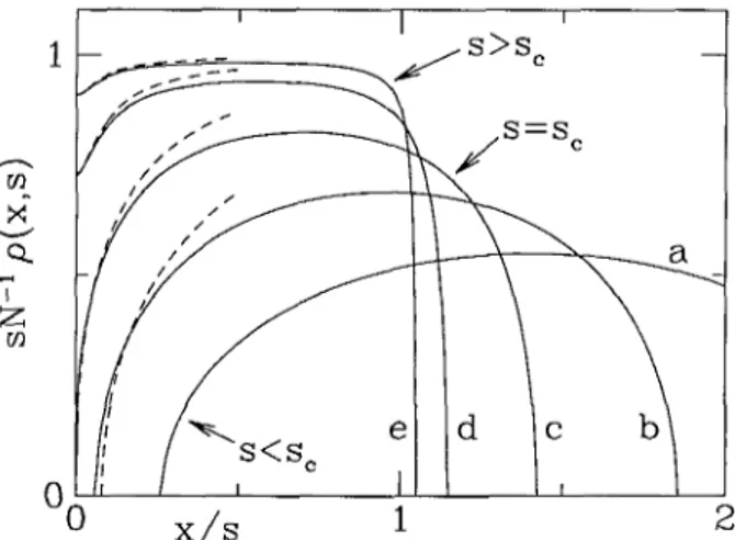
Fig 9 Eigenvalue density p(x, s) äs a function of χ (m units of s = i/i) foi Γ = 0 l Cuives a,b,c,d,e are for s = 2,4, 9, 30,100, respectively The solid curves are ftom eq ("> 8), Ihe dashed cuives ftom eq (5 12) The collision of the density piofile with the boundary at χ — 0, foi s = sc = (l — Γ)/Γ, Signals the disorder-mduced openmg of tunnehng channels responsible foi the
leflectionless tunnehng effect (Fiom ref [54])
on a mapping of eq. (5 7) onto Euler's equation for the isobanc flow of a two-dimensional ideal fluid· L corresponds to time and p to the 7/-component of the velocity field on the x-axis. [Please note that in this section χ is the auxihary variable defined in eq. (5 4) and not the physical coordmate in fig. 2 ] The result is
\lmU(x-iQ+,s), (5.8)
(59)
(5.10) p(x,s) =
where the complex funcüon U(z, s) is determmed by U(z,s) = U0(z-sU(z,s)).
The function t/o (z) is fixed by the initial condition, p0(x')
U0(z] = dx'·
smh2 z — smh x'
The imphcit equation (5.9) has multiple Solutions in the entire complex plane; We need the solution for which both z and z — sU(z, s) he in the stnp between the lines y = 0 and y = —π/2, where z — χ + iy.
The initial condition (5.6) corresponds to
Quantum Transport in Semiconductor-Superconductor Microjunctions 305
The lesulting density (5 8) is plotted m fig 9 (solid curves), for Γ = 01 and seveial values of s Foi s S> l and χ -C s it simphfies to
χ = ^arccoshr — |Γ«(τ2 — l)1'2 cos σ,
σ = TrsN~ p(x, s), τ = a(Ts sin σ)"1, (512) shown dashed in fig 9 Equation (5 12) agrees with the lesult of a Gieen's func-tion calculafunc-tion by Nazarov [30] Foi s = 0 (no disordei), p is a delta function at TQ On adding disorder the eigenvalue density lapidly spieads along the τ-axis (cuive a), such that p < N/s for s > 0 The sharp edges of the density piofile, so uncharactenstic for a ditfusion profile, reveal the hydiodynamic nature of the scahng equation (5 7) The uppei edge is at
Smce L/x has the physical significance of a locahzation length [34], this uppei edge coiiesponds to a mmimum locahzation length £mm = L/xm^x of otder /
The lower edge at xm m propagates fiom TQ to 0 in a "time" sc = (l — Γ)/Γ For
l <C s < sc one has
Xmm = |arccosh(sc/s) - |[1 - (s/Sc)2]1/2 (5 14) It follows that the maximum locahzation length £max = L/xmm mcreases if
disoidei is added to a tunnel junction This paradoxical lesult, that disoidei en-hances tiansmission, becomes intuitively obvious fiom the hydrodynamic cories-pondence, which implies that p(x, s) spieads both to larger and smallei τ äs the fictitious time s piogresses When s = sc the diffusion piofile hits the boundaiy at χ = 0 (cuive c), so that xm m = 0 This implies that for s > sc theie
ex-ist scattenng states (eigenfunctions of ίί^) which tunnel thiough the barner with near-umt transmission probabihty, even if Γ <C l The number Nopen of
trans-mission eigen values close to one (open channels) is of the oider of the numbei of xn's in the ränge 0 to l (smce Tn = 1/cosh2 xn vamshes exponentially if xn > 1) Foi s ^> sc (curve e) we estimate
/V ^ « ( O s1) — N( i + T~1}~~1 (5 1 5Ί
•'"Opel! r^\ ) / \ i^ 1 1 \ ^/
wheie we have used eq (5 12) The disorder mduced opening of tunnelmg chan-nels was discovered by Nazarov [30] It is the fundamental mechamsm for the Γ^2 to Γ"1 transition m the conductance of an NS junction, äs we now discuss
Accoidmg to eqs (2 22), (2 23), (5 4), and (5 5), the aveiage conductances (GNS) and (GN) aie given by the Integrals
4e2 f°°
(GNS) = — / d x p ( x , s ) c o s h ~22 z , (516)
" Ja 2e2 i°°
306 C WJ Beenakker
Here we have used the same tngonometnc identity äs m eq (4 1) For Γ ^> l/L
one is m the regime s » sc of curve e in fig 9 Then the dominant contnbution to the mtegrals comes from the ränge x/s <C l where p(x, s) « p(0, s) = N(s + Γ"1)^1 is approximately mdependent of χ Substitution of p(x, s) by p(0, s) in
eqs (5 16) and (5 17) yields directly
(GNS) « <GN) » Wass, (5 18)
m agreement with the result (5 3) of the numencal simulations
Equation (5 18) has the linear Γ dependence charactenstic for reflectionless tunneling The crossover to the quadratic Γ dependence when Γ < l/ L is obtamed by evaluating the mtegrals (5 16) and (5 17) with the density p ( x , s) given by eq (5 8) The result is [54]
+ Q-1r1, (519)
+ T-1)-1 (520)
The "effective" tunnel probability Q is defined by
Q = - n U - T(l + s m 0 ) - l , (521)
s cos θ \FscosO J
where θ E (Ο, π/2) is the solution of the transcendental equation
-sin0)] =rscos6l (522)
For Γ < l (or s » 1) eqs (521) and (522) simplify to Q - Fsmö,
θ = Fs cos Θ, in precise agreement with the Green's function calculation of Volkov, Zaftsev, and Klapwijk [52] According to eq (5 20), the normal state resistance mcreases linearly with the length L of the disordered region, äs ex-pected from Ohm's law This classical reasoning falls if one of the contacts is m the superconductmg state The scahng of the resistance ANS = I/(GNS) with length, computed from eq (5 19), is plotted m fig 10 For Γ = l the resistance mcreases monotomcally with L The balhstic hmit L — > 0 equals h/4Ne2, half the contact resistance of a normal junction because ot Andreev reflection (cf sec-tion 31) For Γ < 0 5 a resistance mmimum develops, somewhat below L = 1/Γ
The resistance mmimum is associated with the crossover from a quadratic to a linear dependence of /UNS on 1/Γ
If Fs ^> l one has θ — > π/2, hence Q — > Γ In the opposite regime Fs ^C l one has θ — * Fs, hence Q — > F2s The corresponding asymptotic expressions foi
(GNS) are (assuming Γ <C l and s » 1)
+ r-1)-1, if Fs » l, (523)
Quantum Transport in Semiconductor-Superconductor Microjunctwns 307
0
Fig 10 Dependence of the resistance ANS on the length L of the disordered noimal region (hatched
m the mset), for different values of the transmittance Γ of the NS Interface Solid curves are computed ftom eq (5 19), for Γ = l 0 8, 0 6, 0 4 0 l ftom bottom to top Foi Γ <C l the dashed curve is appioached (Fiom lef [54] )
In either hmit the conductance is gieater than the classical result
Gc^ss = (2Ne2/h)(s + 2Γ-2)-1, (525)
which holds if phase coherence between electrons and holes is destroyed by a voltage or magnetic field The peak m the conductance around V, B = 0 is of order AÖNS = (GNS) — G>]gss, which has the relative magnitude
AGNS
(G:
NS;
(526)The scalmg theory assumes zero temperature Hekkmg and Nazarov [53] have studied the conductance of a resistive NS Interface at finite temperatures, when L is greater than the correlation length Lc = mm (Ιφ, ^/hD/k^T) Their result is consistent with the hmiting expression (5 24), if s = L/l is icplaced by Lc/l
The imphcation is that, if L > Lc, the non-hnear scalmg of the resistance shown
in fig 10 only applies to a disordered segment of length Lc adjacent to the
308 C WJ Beenakker
5 3 Double-barner junction
In the previous subsection we have discussed how the opening of tunnelmg chan-nels (i e the appearance of transmission eigenvalues close to one) by disorder leads to a minimum m the resistance when L ~ //Γ The mmimum separates a Γ"1
from a Γ~2 dependence of the resistance on the transparency of the Interface We
lefeued to the Γ"1 dependence äs "reflectionless tunnelmg", smce it is äs if one of
the two quasiparticles which form the Cooper pair can tunnel thiough the baruei with piobabihty one In the present subsection we will show, followmg lef [62], that a quahtatively similai effect occuis if the disordei in the noimal legion is le-placed by a second tunnel barner (tunnel piobabihty Γ") The lesistance at fixed Γ shows a minimum äs a function of Γ" when Γ' ~ Γ For Γ' < Γ the resistance has a Γ^1 dependence, so that we can speak agam of reflectionless tunnelmg
We considei an NIiNI^S junction, wheie N = normal metal, S = supeicon-ductoi, and Ιτ = insulatoi or tunnel barner (transmission piobabihty pei mode
ΓΙ Ξ l/ cosh2 cO We assume ballistic motion between the baineis (The effect
of disoidei is discussed later) A sti aightforward calculation yields the transmis-sion probabihües Tn of the two barners m senes,
1
,
(527)
<? — 2 + 2 cosh 1a\ cosh 2a2, b = ^ smh 2a^ sinh 2a2, (5 28)
where ψη is the phase accumulated between the barners by mode n Smce the
transmission matnx f is diagonal, the tiansmission probabihties Tn are identical
to the eigenvalues of ttf We assume that L J> Ar (Ar is the Feimi wavelength) and A/T, S> l, so that the conductance is not dommated by a smgle lesonance In this case, the phases φη are distnbuted umformly in the interval (Ο, 2π) and we
may replace the sum ovei the transmission eigenvalues m eqs (2 22) and (2 23) by Integrals over φ Ση=ι f((fri} ~^ (Ν/2π) JQ π αφ f((p] The result is
47Ve2 cosh 2cni cosh 2a2
<^NS = — ; -- 575-, (529)
11 (cosh2 2«! + cosh2 2a2 - l) '
47Ve2
+cosh2a2)~1 (530)
n/
These expressions are symmettic in the mdices l and 2 It does not mattei which of the two bainers is closest to the superconductoi In the same way we can com-pute the entne distnbution of the transmission eigenvalues, p(T) = Σ
Tn) -> (Ν/2π) /02π αφ δ (Τ -Τ (φ)) Substitutmg T (φ) = (a + öcostp)^1 from
eq (5 27), one finds
Quantum Transport m Semiconductor-Superconductor Microjunctions 309
10
W
CD cv
C\2 X
0
Γ
2=0 l
N
N
S
10
20Fig U Dependence of the resistances AN and ANS of balhstic NININ and MINIS stiuctuies, icspectively, on barnei tiansparency ΓΙ, whilc tiansparency Γ^ = 0 l is kept fixed [computed fiom eqs ('S 29) and (5 30)] The msct shows the NINIS stuictuie consideied (Fiom ref [62] )
In fig 11 we plot the resistance AN : from eqs (5 29) and (5 30) Notice that.
;* (1/Ti + 1/Γ2 - 1),
and /UNS = follows Ohm's law,
followmg
(532)
äs expected from classical considerations In contrast, the resistance ANS has a mimmum if one of the PS is varied while keeping the other fixed This resistance mimmum cannot be explamed by classical senes addition of barrier resistances If Γ2 <C l is fixed and ΓΙ is varied, äs in fig 11, the mimmum occurs when ΓΙ = \/2 Γ 2 The minimal resistance -R^s" is of the same order of magmtude äs the resistance AN in the noimal state at the same value of ΓΙ and Γ2 In paiticular, we find that R^™ depends linearly on 1/Γ\, whereas for a single bariier ANS oc l/Γ2
densit-310 C WJ Beenakker
l
2
0
(a)
(b)
0
0.5
T
0
0.5
T
Fig 12 Density of transmission eigenvalues through a normal region contaming a potential bainei (tiansmission piobabihty Γ = 0 4) The left panel (a) shows the disorder mduced openmg of tunnel mg channels (sohd curve s = 0 04 dotted s = 0 4, dashed s = 5 where s Ξ L / l ) The nght panel (b) shows the openmg of channels by a second tunnel bainei (transpaiency Γ", solid cuive Γ' = 0 95, dotted Γ' = 0 8, dashed Γ' = 0 4) The curves m (a) are computed fiom eq (5 8) the curves m (b) from eq (531) (From ref [62])
ies of normal-state transmission eigenvalues The left panel is foi an NIS junction [computed usmg eq (5 8)], the nght panel is for an NINIS junction [computed from eq (5 31)] In the NIS junction, disorder leads to a bimodal distnbution p(T), with a peak near zero transmission and another peak near unit transmiss-sion (dashed curve) A similar bimodal distnbution appears in the ballistic NINIS junction, for approximately equal transmission probabihties of the two bainers
There are also differences between the two cases The NIS junction has a uni-modal p(T) ifL/l < 1/Γ, while the NINIS junction has a bimodal p(T) foi any ratio of ΓΙ and Γ2 In both cases, the openmg of tunnehng channels, i e the ap-pearance of a peak in p(T) near T = l, is the origin for the 1/Γ dependence of the resistance
Quantum Transport m Senuconductor-Superconductor Micmjunctions 311
(Γι, Γ2 <C 1) and strong disorder (L ^$> l), one has the two asymptotic foimulas Ο Λ Γ „2
GNS = -f -- ^- , if Γ! , Γ2 « //i, (5 33)
h (Γ2+Γ1)3
GNS = (i/^ + Ι/Γι + 1/Γ2)"1, if Γ ι , Γ2» ί / - & (534)
Equation (5 33) comcides with eq (5 29) in the limit a\ , a2 3> l (recall that Tt Ξ l / cosh2 al ) This shows that the eftect of disorder on the resistance minimum can be neglected äs long äs the resistance of the junction is dommated by the barneis In this case GNS depends Imearly on ΓΙ and Γ2 only if ΓΙ « Γ2 Equation (5 34) shows that if the disorder dommates, GNS has a linear Γ-dependence legardless of the relative magnitude of ΓΙ and Γ2
We have assumed zero temperature, zero magnetic field, and infinitesimal ap-phed voltage Each of these quantities is capable of destroymg the phase coher-ence between the electrons and the Andreev-reflected holes, which is respons-ible foi the resistance mmimum As far äs the temperature T and voltage V are concerned, we require k&T, eV <C fi,/Tdweii for the appearance of a resistance
minimum, where Tdweii is the dwell time of an electron in the region between
the two barners For a balhstic NINIS junction Tdweii — L/υγΤ, while foi a disordered junction Tdweii — L2 /vpTl is larger by a factor L/l It follows that
the condition on temperature and voltage becomes more restnctive if the disorder increases, even if the resistance remams dommated by the barners As far äs the magnetic field B is concerned, we lequire B <c h/eS (with S the area of the junction perpendicular to B), if the motion between the barriers is diffusive For balhstic motion the trajectories enclose no flux, so no magnetic field dependence is expected
A possible expenment to venfy these results might be scanmng tunnehng mi-cioscopy (STM) of a metal particle on a superconducting Substrate [63] The metal-superconductor Interface has a fixed tunnel probability Γ2 The probabil-ity ΓΙ for an electron to tunnel from STM to particle can be controlled by varymg the distance (Volkov has recently analyzed this geometry in the legime that the motion from STM to particle is diffusive rather than by tunnehng [64] ) Anothei possibihty is to create an NINIS junction usmg a two-dimensional electron gas in contact with a superconductor An adjustable tunnel barner could then be imple-mented by means of a gate electrode
5 4 Circuit theory
312 CWJ Beenakker
theory for the diffusive regime was presented recently by Nazarov [65] Startmg from a conünuity equation for the Keldysh Green's function [66], and applymg the appropnate boundary conditions [67], Nazarov was able to formulate a set of rules which reduce the problem of Computing the resistance of an NS junc-tion to a simple exercise in Circuit theory Furthermore, the approach can be ap-phed without further complications to multi-termmal networks involving several normal and superconductmg reservoirs Because of its practical importance, we discuss Nazarov's Circuit theory in some detail
The supeiconductors 5, should all be at the same voltage, but may have a dif-ferent phase φι of the pair potential Zero temperature is assumed, äs well äs
infinitesimal voltage differences between the normal reservoirs (linear response) The reservoirs are connected by a set of diffusive normal-state conductors (length Lt, mean free path lt, sl = L»//t > 1) Between the conductors there may be
tunnel barners (tunnel probability FJ The presence of superconductmg reser-voirs has no effect on the resistance (h/2Ne2)si of the diffusive conductors, but affects only the resistance h/2Ne2T';fi of the tunnel barners The tunnel probab-ility Γ ι of barner i is renormahzed to an effective tunnel probability Ff, which depends on the entire Circuit
Nazarov's rules to compute the effective tunnel probabilities are äs follows To each node and to each termmal of the Circuit one assigns a vector n% of unit length For a normal reservoir, ητ = (0, 0,1) is at the north pole, for a superconductmg
reservoir, n, = (cos φ^, sin φ^ 0) is at the equator For a node, n% is somewhere
on the northern hemisphere The vector nr is called a "spectral vector", because it
is a particular parametenzation of the local energy spectrum If the tunnel barner is located between spectral vectors n\ and n^, its effective tunnel probability is*
Feff = (m η2)Γ = Γ cos Öi2, (5 35)
where #12 is the angle between rii and η·2 The rule to compute the spectral vector of node ι follows from the contmuity equation for the Green's function Let the index k label the nodes or termmals connected to node ι by a single tunnel barner (with tunnel probability Γ&) Let the mdex q label the nodes or termmals connected to ι by a diffusive conductor (with L/l = sq) The spectral vectors
then satisfy the sum rule [65]
Σ
τ—·., % arccosfrii na)(n, χ nk)Tk + £(n, x nq] \ q> = 0 (5 36)
k g Sq^L-^ nq)
This is a sum rule for a set of vectors perpendicular to ητ of magnitude F^ sin 9lk
or Olq/$q, depending on whether the element connected to node ι is a tunnel
* It may happen that cos θ\ι < 0, m which case the effective tunnel probability is negative Nazaiov has given an example of a four-termmal Circuit with Feff < 0, so that the current through this banier
Quantum Transport in Semiconductor-Superconductor Micmjunctions 313
os
IN
' A
N
Fig. 13. At left: Circuit containing two terminals (open circles), one node (filled circle), and two elements: A diffusive conductor (shaded) and a tunncl barrier (black). At right: Spectral vectors associated with the terminals N,S and with the node A.
barrier or a diffusive conductor. There is a sum rule for each node, and together the sum rules determine the spectral vectors of the nodes.
As a simple example, let us consider the System of section 5.2, consisling of one normal terminal (N), one superconducting terminal (S), one node (labeled A), and two elements: A diffusive conductor (with L/l = s) between N and A, and a tunnel barrier (tunnel probability Γ) between A and S (see fig. 13). There are three spectral vectors, ΠΝ, η$, and ΠΑ- All spectral vectors lie in one plane. (This holds for any network with a single superconducting terminal.) The resistance of the circuit is given by R = (h/2Ne2)(s + l/Fe f f), with the effective tunnel
probability
reff = rcos6>A S = rsin0. (5.37)
Here θ e [Ο, π/2] is the polar angle of ΠΑ- This angle is determined by the sum rule (5.36), which in this case takes the form
Γ cos 6»-6i/s = 0. (5.38)
Comparison with section 5.2 shows that Feff coincides with the effective tunnel
probability Q of eq. (5.21) in the limit s ^> l, i.e. if one restricts oneself to the diffusive regime. That is the basic requirement for the application of the circuit theory.
Let us now consider the "fork junction" of fig. 14, with one normal terminal (N) and two superconducting terminals Si and S2 (phases φι = -φ/2 and φ2 = Φ/2}.
314 C.W.J. Beenakker
O S
OS
Fig 14. Circuit diagram and spectral vectors for a structure contaming one normal and two super-conducting terminals (phase difference φ).
theoretically by Hekking and Nazarov [53] and experimentally by Pothier et al. [69]. For simplicity, let us assume two identical tunnel barriers T\ = Τ·2 = Γ. Then the spectral vector ΠΑ = (sin (9, 0,cosö) of node A lies symmetrically between the spectral vectors of terminals Sj and 83. The sum rule (5.36) now takes the form
2r|cos|0|cos6>-ö/s = 0. (5.39)
Its solution determines the effective tunnel rate Feff = Γ| cos \φ\ sin θ of each of the two barriers in parallel, and hence the conductance of the fork junction,
G = Ί-ΙΙ-Ι
h
Two limiting cases of eqs. (5.39) and (5.40) are
if
cos
cos <
(5.40)
(5.41)
: 1. (5.42) For φ = 0 (and 2Γ —» Γ) these expressions reduce to the results (5.23) and (5.24) for an NS junction with a single superconducting reservoir. The limit (5.42) agrees with the finite-temperature result of Hekking and Nazarov [53], if s is replaced by
Lc/l and a series resistance is added due to the normal segment which is further than a correlation length from the NS interfaces. The possibility of a dependence of the conductance on the superconducting phase difference was noted also in other theoretical works, for different geometries [70-75],
Quantum Transport in Semiconductor-Superconductor Micmjunctions 315
8
6
"l 4 'ο
2
T=30mK, ν=4.1μν
-0.4 -0.2
0.0
B (mT)
0.2 0.4
Fig l S Conductance of a fork junction äs a function of magnetic field, showmg the dependence on the phase difference φ of the superconductor at two tunnel barners The circles are measurements by Pothiei et al [69] of the current / through a Cu wire connected to an oxidized AI fork (normal-state resistance AN = l 56 kü) The apphed voltage V is sufficiently low that I/V is close to the
hnear-iesponse conductance (The amphtude of the oscillations at V = 0 is 3 94 χ 10~6Ω~1,
somewhat larger than m the figure ) The solid curve is a cosme fit to the data The offset of maximum conductance from B = 0 is attubuted to a small residual field m the cryostat (Courtesy of H Pothier)
conductance of a Cu wire attached to an oxidized AI fork oscillates äs a function of the apphed magnetic field. The penod corresponds to a flux mcrement of h/2e through the area enclosed by the fork and the wire, and thus to Αφ = 2π. The expenment is m the regime where the junction resistance is dommated by the tun-nel barners, äs m eq. (5.42).* The metal-oxide tunnel barners m such structures have typically very small transmission probabihties (Γ ~ 10~5 in ref. [69]), so that the regime of eq (5.41) is not easily accessible. Larger F's can be reahzed by the Schottky barner at a semiconductor — superconductor Interface It would be of mterest to observe the crossover with mcreasmg Γ to the non-smusoidal (/>-dependence predicted by eq. (5.41), äs a further lest of the theory.
316 C WJ Beenakker
6. Universal conductance fluctuations
So far we have considered the average of the conductance over an ensemble ot impunty potentials In fig 16 we show results of numencal simulations [39] for the vanance of the sample-to-sample fluctuations of the conductance, äs a function of the average conductance in the normal state A ränge of parameters i, W, l, N was used to collect this data, in the quasi-one-dimensional, metalhc, diffusive regime l < W < L < Nl An ideal NS mterface was assumed (Γ = 1) The results for VarGN are äs expected theoretically [34,35] for "universal conductance fluctuations" (UCF)
VarGN = ^/3-1(e2/^)2 (61)
lo
The index β equals l m the presence and 2 m the absence of time-ieversal sym-metry The l/ β dependence of Var GN implies that the vanance of the conduct-ance fluctuations is reduced by a factor of two upon application of a magnetic field, äs observed in the Simulation (see the two dotted Imes in the lowei part of fig 16) The data for Var GNS at 5 = 0 shows approximately a four-told m-crease over Var GN For B φ 0, the Simulation shows that Var GNS ls essentially
unaffected by a time-reversal-symmetry breaking magnetic field In contrast to the Situation in the normal state, the theory for UCF m an NS junction is quite different for zero and for non-zero magnetic field, äs we now discuss
In zero magnetic field, the conductance of the NS junction is given by eq (2 22), which is an expression of the form A = Ση a(Tn) Such a quantity A is called a linear statistic on the transmission eigenvalues The word "linear" refers to the fact that A does not contam products of different T„'s The function a(T) may well depend non-lmearly on T, äs it does for GNS, where a(T) is a rational function of T The Landauer formula (2 23) for the normal-state conductance is also a linear statistic, with α(-Γ) ex T It is a general theorem in random-matnx theory [76] that the vanance of a linear statistic has a l/ß dependence on the
symmetry index β Moreover, the magnitude of the vanance is mdependent of the microscopic properties of the System (sample size, degree of disorder) This is Imry's fundamental explanation for UCF [28]
For a wire geometry, there exists a formula for the vanance of an arbitrary linear statistic [37,77,78],
v
Λ
Quantum Transport m Semiconductor-Superconductor Microjunctions 317
eö
Χ Χ
"V
^
NS
Ν
+H-+
X X X χ Χ<
_1 ι t [_
χ
10
20
Fig 16 Numencal calculation of the vanance of the fluctuations m GN and GNS> as a function
of the aveiage GN (+ foi B = Ο, χ foi a flux of 10 h/e) Dotted hnes aie the analytical lesults fiom eqs (6 1) and (6 3) Note the absence of a facloi of two leductton m Var GNS on applymg a
magnetic field (From lef [39])
where α (T) — arccoshT :/2 In the normal state, Substitution of a(T) = (2e2//i)T into eq (6 2) reproduces the result (6 1) In the NS junction, substitu-tionof a(T) = (te2 / h)T2 (2 - T)~2 yields, for the case β = l of zero magnetic field,
32
VarGN S = — (2-iü
)2 = 4 3 0 V a r G (63)
A factoi of foui between Var GNS and Vai GN was estimated by Takane and
Ebisawa [33], by an argument similar to that which we descnbed in section 4 for the weak-localization correction (A diagrammatic calculation by the same authors [79] gave a factor of six, presumably because only the dominant diagiam was included ) The numencal data in fig 16 is within 10 % of the theoietical prediction (6 3) (upper dotted Ime) Similar numencal results for Var GNS m
zero magnetic field weie obtamed m refs [33,80]
![Fig 3 Solid curve Conductance GNS veisus Feimi energy of a quanlum pomt contact between a noimal and a supeiconductmg teseivoir (shown schematically m the inset) The dotted cuive is twice the conductance GN forthe case of two noimal reservons [20] The cons](https://thumb-us.123doks.com/thumbv2/123dok_us/8292973.2196121/15.610.127.432.68.393/conductance-quanlum-contact-supeiconductmg-teseivoir-schematically-conductance-reservons.webp)
![Fig 8 Fillecl circles Numencally calculated resistance ANS of a disordered NS ]unction versus Ihe Uansmission probabüity per mode Γ of the tunnel barner at the NS mterface Open ciicles Resistance AN of the same junction in the normal state (a) is for zero](https://thumb-us.123doks.com/thumbv2/123dok_us/8292973.2196121/24.633.126.508.77.333/numencally-calculated-resistance-disordered-uansmission-probabüity-mterface-resistance.webp)