Titanium Doped ITO Thin Films Produced by Sputtering Method
Leandro Voisin
1, Makoto Ohtsuka
2;*and Takashi Nakamura
21New Industry Creation Hatchery Center, Tohoku University, Sendai 980-8579, Japan
2Institute of Multidisciplinary Research for Advanced Materials, Tohoku University, Sendai 980-8577, Japan
Indium-tin-oxide (ITO) thin films, typically produced by In2O3-10 mass%SnO2 target, are widely used for the elaboration of optoelectronics devices such as liquid crystal displays (LCD), flat panel displays (FPD), plasma displays, touch panels, etc., and they are required to satisfied specific optoelectronical properties such as, low volume resistivity and high transmittance.
Due to the current high cost and limited supply of indium, titanium was investigated as dopant element for the production of ITO thin films. Two sputtering method were carried out; a combinatorial method where an In2O3-10 mass%SnO2and a Ti targets were simultaneously sputtered and then a co-sputtering method where, in addition to the previous targets, an In2O3-50 mass%SnO2and a TiO2targets were also sputtered.
Effects of the oxygen flow and heat treatment temperature on the optoelectronical properties of ITO thin films doped with Ti, as metal and dioxide, were investigated and the results were discussed on the basis of crystallization for bixbyte structure of In2O3. The obtained results indicate that the use of Ti as dopant element during the production of ITO thin films by sputtering method will be promising.
[doi:10.2320/matertrans.MBW200907]
(Received October 15, 2009; Accepted December 7, 2009; Published January 27, 2010)
Keywords: titanium doped indium-tin-oxide thin film, combinatorial sputtering method, volume resistivity, transmittance
1. Introduction
Indium-tin-oxide (ITO) thin films are widely used as transparent conductive coating during the elaboration of optoelectronics devices such as liquid crystal displays (LCD), flat panel displays (FPD),1) plasma displays, touch panels, electronic ink applications, solar cells,2) antistatic coating and organic light emitting devices (OLED).3) The typical ITO target used for the sputtering method presents a composition of In2O3-10 mass%SnO2 and their produced
thin films are required to satisfied specific values for several properties such as high electrical conductivity, , (1000mS), high optical transmittance, , in the visible region of the spectrum (>85%, 400800nm), satisfactory etching quality, etc.4)
Since in recent times ITO has expected an increasing demand with the popularity of LCD computer monitors and televisions, the indium world supply is becoming scarce causing an important rise in its price. The amount of indium consumed is largely a function of worldwide ITO thin films production. Worldwide production of indium is currently 480 and 650 tons per year from mining and recycling, respec-tively.5)
The recent changes in demand and supply have resulted in high and fluctuating prices of indium, which from 2002 to 2007 ranged from US$95/kg to US$1000/kg with a current price around US$510/kg.6)Demand for indium is expected to increase back with the actual increasing demand for ITO thin films for LCD production and with large-scale manufacture of copper indium gallium (di)selenide (CIGS)-based thin film solar technology starting by several companies since 2008.
Based on content of indium in zinc ore stocks, there is a worldwide reserve base of approximately 6000 tons of economically-viable indium.7)This value has led to estimates suggesting that, at current consumption rates, there is only 13 years supply of indium left,8)which certainly represents a
strong negative environmental impact because its premature depletion. Therefore, in order to decrease the use of indium during the production of ITO films, a new target, which considers a smaller quantity of In2O3in its composition and
that it maintains or improved the related properties is required to be developed.
Titanium is a transition metal, which could be a suitable substitution or dopant element for the production of ITO thin films due to its quite low electrical volume resistivity, V, 0.42mm, relatively high transmittance and the excellent resistance to corrosion for its (IV) oxide.9) In addition, titanium is the ninth-most abundant element in the Earth’s crust (0.63 mass%)9)and its actual commercial price is about US$19/kg6)25 times cheaper than that of indium.
In the present research, the production of titanium-doped ITO thin films by using the sputtering method was inves-tigated for developing a new target, which considers a lower content of indium. The effect of the heat treatment on the sputtered films was also investigated.
2. Experimental Method and Procedure
A schematic diagram of the sputtering apparatus (ULVAC, CS-200) used in the present study is shown in Fig. 1. Thin films were deposited on glass substrates (Corning EAGLE 2000, surface: 50mm50mm, thickness: 0.7 mm). Two sputtering method were carried out; a combinatorial method where an In2O3-10 mass%SnO2 (ITO [90]) and a Ti targets
were simultaneously sputtered and then a co-sputtering method where, in addition to the previous targets, an In2O3-50 mass%SnO2 (ITO [50]) and a TiO2 targets were
also later sputtered. A brief description and the corresponding sputtering condition for each method are explained in sections 2.1 and 2.2 while their schematic diagrams are shown in Figs. 2 (a) and (b), respectively.
To sputter the ITO targets a resonance circuit (L/C) filter to eliminate ripple frequencies, an active arc killer (A2K) to prevent abnormal discharge, and a direct current (DC) power
source were available, while for Ti targets a matching box (M/BOX) and a high radio frequency (RF) power source were used. Process chamber was vacuum at 105Pa for
its base pressure while total experimental pressures were resulted to be between 0.67 and 0.7 Pa.
The effects of the oxygen flow,Q(O2), and heat treatment
temperature,THT, on the optoelectronical properties ofand Vfor the ITO thin films doped with Ti, as metal and dioxide, were investigated and compared against those previously obtained by the authors10)for the ITO [90] thin film produced under the gas flow ratio condition of argon to oxygen, (Q(Ar)/Q(O2)), = 50/0.2, which resulted to be the best
condition for that material.
The measurements ofVwere carried out with a resistivity meter (Mitsubishi chemical analytech, Loresta GP Model MCP-T610) by using a 4-terminal method, while were measured into the 200900 nm range of wavelength () by using a Spectrophotometer (Hitachi High-Tech, U-3900H). For the latter, a glass substrate resulted to reach around 92% in the range of wavelength,, between 350 and 1000 nm, this measurement and those for the obtained thin films were taken by consider air as reference.
2.1 Combinatorial sputtering method
By using the combinatorial sputtering method a compo-sition gradient Ti doped ITO thin film can be produced on a substrate glass since both ITO [90] and high purity metallic Ti targets are sputtered at the same time keeping fixed the substrate holder during the deposition (Fig. 2 (a)).
For combinatorial sputtered experiments, the substrate glass was located on the center of the substrate holder, at the point equidistant from ITO [90] and Ti targets, (Q(Ar)/Q(O2)) was
set at 50/0.2 and sputtering time at 1.8 ks.
For the production of the ITO [90] film, the DC power source was fixed at 100 W and when the combinatorial sputtering method was applied in addition to the latter, the RF power source was set at 50 W for Ti.
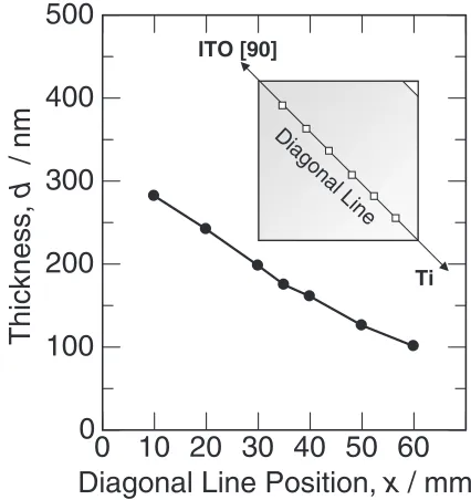
In order to determine the gradient of thickness,d, for the obtained films, a very thin line of about 50mmof width and 1 mm of length was removed with a laser in six aligned positions, x, separated 10 mm to each other and located along the diagonal line between the targets and thend, was measured in each of those positions by using a scanning probe microscope (SPM, SII L-trace II), under dynamic force mode (DFM). The relation betweendandxfor the Ti doped ITO [90] film is shown in Fig. 3.
Finally, the produced films were heat treated at 523 K for 3.6 ks (HT523) and by using the obtained thickness informa-tion, their composition and optoelectronical properties were determined for both as deposited, as-depo., and heat treated, HT, conditions.
2.2 Co-sputtering method
The co-sputtering method corresponds to simultaneously sputter the two target cathodes under the rotation of the substrate holder in order to obtain a homogeneous deposition of mixed composition (Fig. 2 (b)). In this research, two cases were considered; the simultaneous sputtering of the ITO [90] with the pure metallic Ti targets, and that of the ITO [50] with the TiO2targets. Rotation speed for the substrate holder was
set to 40 rpm.
Deposition rates were determined by sputtering each single target at two different powers for 1.8 ks and later measuring the thickness of the obtained films by using a SPM as it was previously explained in Section 2.1. In order to produce Substrate
Holder
L/C filter
DC power (100 W)
4 elem. target Ti / TiO2
RF power (20~100 W)
M/BOX
Active arc killer (A2K) ITO target
[90] / [50]
Process Chamber
th
Fig. 1 Schematic diagram of the sputtering apparatus.
Ti
ITO ITO
(b) (a)
no rotation rotation
Substrate holder
Glass substrate
Glass substrates
Ti, TiO2
Fig. 2 Schematic diagram of sputtering methods. (a) Combinatorial and (b) co-sputtering.
0
10 20 30 40 50 60
0
100
200
300
400
500
Diagonal Line Position, x / mm
Thickness,
d
/ nm
ITO [90]
Ti Diagonal Line
[image:2.595.319.532.75.301.2] [image:2.595.63.275.77.233.2] [image:2.595.62.275.268.395.2]films with a standard thickness of about 150 nm and a mass% of In2O3 close to 48, DC power was fixed to 100 W for ITO
targets, RF power was fixed to 100 and 20 W for Ti and TiO2
target while sputtering time was set to 20 and 28 min for ITO [90]–Ti and for ITO [50]–TiO2 co-sputtered experiments,
respectively.
To determine the effect of Q(O2) on V, three different levels forQ(O2) of 0.2, 0.3 and 0.4, and 0, 0.2 and 0.3 sccm
were investigated for ITO [90]–Ti and ITO [50]–TiO2
co-sputtered experiments, respectively. Q(Ar) was fixed to 50 sccm for all the experiments.
As is shown in Fig. 2 (b), six glasses were concentrically set on the substrate holder, one film was kept for as-depo. condition, while the other five ones were later heat treated, HT, by separated at 523, 623, 723, 823 and 923 K, respectively to investigate the effect of the THT, on the optoelectronical properties of ITO thin films doped with Ti, as metal and dioxide.
3. Results and Discussions
The effects of Q(O2) and THT on the optoelectronical properties of,Vandfor the ITO thin films doped with Ti, as metal and dioxide, were investigated and the results were compared to those previously obtained by the authors10) for the ITO [90] thin film and discussed on the basis of crystallization for bixbyte structure of In2O3.
3.1 Ti doped ITO thin films produced by combinatorial method
was measured in six aligned positions, x, on the films separated 10 mm each other and located along the diagonal line between the targets. The results of, for the ITO [90] and Ti doped ITO [90] as-depo. and HT523 films are shown together in relation to x in Fig. 4. With increasing the distance from the ITO [90] target, decreases from 50 to 3.7 mS and from 21 to 0.03 mS in the ITO [90] and, Ti doped ITO [90] as-depo. films, respectively. It is considered that this difference in the latter may be ascribed to the stronger chemical affinity of oxygen for titanium than that for indium, thus the ITO [90] as-depo. film is reduced by the titanium resulting in the formation of the lower conductive InO.
When the heat treatment was applied to the ITO [90] film,
resulted to be slightly decreased in the region close to the ITO [90] target but it was half order improved in the far away part. On the other hand, on the Ti-doped ITO [90] film, it causes an important improvement ofin the whole region, reaching even two orders of difference in the region close to the Ti target, this effect may be ascribed to the decrease of black indium monoxide (InO) in the film because the oxygen vacancy becomes filled under air atmosphere.
was measured for the ITO [90] and Ti doped ITO [90] as-depo. and HT523 films on the their lower-right part through a square area which was indicated with dashed line in Fig. 5. According to those results,is about 80 and 85% in the visible region of the spectrum (400800nm), for the ITO [90] and Ti-doped ITO [90] as-depo. films, and when the heat treatment was consideredwas improved to about 90 and 88%, respectively. All the results are quite similar in tendency with the exception of that obtained for the ITO [90]
HT523 film, which presents a notorious imperfection in the range of between 400 and 600 nm.
Figure 6 shows the X-ray diffraction (XRD) results measured on the lower-right part of the films obtained by combinatorial sputtering method. According to Fig. 6, as-depo. films result in amorphous structure, nevertheless when heat treatment was applied to the films, five peaks appeared, which can be assigned to the cubic bixbyte structure of In2O3.11) Non SnO2 peaks appeared and the
intensity of the peaks for the HT films was higher in the Ti doped ITO [90] HT523 substrate.
Finally, according to Figs. 4 and 6, it can be observed that there is a clear relationship betweenand crystallization for bixbyte, by heat treated the films, the concentration of dopants, tin or oxygen vacancy trapped at crystalline defects can be decreased, improving bixbyte crystallization and increasing electrically active species inside each grain.
0
10 20 30 40 50 60
10
-210
-110
010
110
210
3Diagonal Line Position, x / mm
as-depo.
HT523
ITO [90]
ITO [90]-Ti
Electrical Conductivity,
σ
/ mS
Fig. 4 Relation betweenandxfor ITO [90] and Ti doped ITO [90] thin films produced by combinatorial sputtering method.
ITO [90] ITO [90]-Ti
200
400
600
800
1000
0
20
40
60
80
100
Wavelength,
λ
/ nm
Transmittance,
τ
(%)
glass as-depo.
HT523
measured area
[image:3.595.323.531.75.302.2] [image:3.595.320.532.359.530.2]3.2 Ti doped ITO thin films produced by co-sputtering method
When the thickness was measured for each co-sputtered film, a barely small difference with a standard deviation between 0.23 and 0.57 depends on the sample was found, thus it was decided to measure three symmetric and equi-distant points on both the left and the right sides of the films, six points in total, and take the average value as the corresponding thickness for each specific film. By using the thickness information, V was later determined for each obtained film.
Figure 7 shows the effects of Q(O2) andTHT on the V measured for the Ti doped ITO [90] films. According to Fig. 7, with increasing Q(O2), in the system V strongly increased for the as-depo. film while for the HT films,
V present quite similar tendencies each other showing a minimum atQ(O2) = 0.3 sccm. It was also observed thatV decreases with increasingTHT, this effect may be ascribed to the improvement of In2O3 bixbyte crystallinity. The
mini-mum value for V of 26.9mm (¼25mS) was obtained from the Ti doped ITO [90] HT923 film. This value is about twice, but still a promising result in comparison to that of
V¼14:3mm (¼48mS) obtained from the ITO [90] HT523 film and showed in the same figure with opened triangle mark.
was measured for the as-depo. and HT523 ITO [90] and Ti doped ITO [90] films under the condition ofQ(Ar)/ Q(O2) = 50/0.2 and 50/0.3, respectively on the their
upper-left part through a square area indicated with dashed line in Fig. 8. According to those results, Ti doped ITO [90] as-depo. film shows awith a concave form and values between
85 and 90% in the range between400550nm reaching later a plateau until the 800 nm. was not affected by temperature in the range between 523 and 923 K and so HT films show an almost identical each other and similar in tendency to that for as-depo. film but increasing the width of the concavity starting from¼350nm. In comparison to ITO [90], Ti doped ITO [90] films present a quite improved
in the range of between 400550nm and a similar tendency but lower of around 8% between550900nm. The improvement in the first range may be ascribed the higher
of titanium dioxide than that of tin dioxide. It is important to note that the for the HT523 ITO [90] film resulted to be higher than that of the glass substrate in the range of
between 600700nm, this effect may be attributed to the reduction of the reflectance on the glass because the presence of the ITO film.
To investigated the effect of directly sputter titanium diox-ide as dopant and compare with the previous results where
10
°
20
°
30
°
40
°
50
°
60
°
70
°
2
θ
(Cu-K
α
)
Intensity,
I
(arb. unit)
In
2O
3(calc.)
α
-Ti (calc.)
as-depo.
HT523
as-depo.
HT523
ITO [90]-Ti
ITO [90]
TiO
2(calc.)
In
2O
3Fig. 6 XRD results for ITO [90] and Ti doped ITO [90] thin films produced by combinatorial sputtering method.
0
0.1
0.2
0.3
0.4
0.5
10
010
110
210
310
410
5Oxygen Flow,
Q
(O
2) / sccm
Volume Resistivity,
ρ
v/
µ Ω
m
as-depo. HT523 HT623
HT723 HT823 HT923
ITO[90]
Fig. 7 Effects ofQ(O2) andTHTon theVof Ti doped ITO [90] thin films
produced by co-sputtering method.
200
0
400
600
800
1000
20
40
60
80
100
Transmittance,
τ
(%)
ITO [90] ITO [90]-Ti
glass
Wavelength,
λ
/ nm
as-depo. HT523
measured area
Fig. 8 Effects ofTHTon theof ITO [90] and Ti doped ITO [90] thin films
[image:4.595.57.278.71.361.2] [image:4.595.321.534.76.280.2] [image:4.595.319.533.336.508.2]metallic Ti was sputtered, TiO2 doped ITO [50] films were
also produced, as it was mentioned before the reason to use an ITO [50] target at this point is exclusively to reduce the content of In2O3 at around 48 mass% for the obtained films.
Figure 9 shows the effects of THT and Q(O2) on the V measured for the TiO2doped ITO [50] films, in addition, the
best results obtained from the Ti doped ITO [90] films, under the conditionQ(Ar)/Q(O2) = 50/0.3, are shown in the same
figure for comparing the effect of using metallic and dioxide titanium as dopant during the sputtering.
According to Fig. 9, the lower V resulted when non-addition of oxygen was considered during the co-sputtering of TiO2 doped ITO [50] films, even more for the as-depo.
films, by the addition of 0.2 and 0.3 sccm of oxygen, V resulted to be increased in the order of 100 and 500 times, respectively. For the HT films,Vpresent similar tendencies each other againstTHT decreasing in the range between 523 to 823 K and then abruptly increasing at 923 K, this tendency may be ascribed to a combined effect because crystallization of films increases with increasing temperature reducing the defect in trap and improving the hall mobility, nevertheless oxygen vacancies became filled under atmosphere pressure at high temperature decreasing the carrier density and then increasing V,12)the latter effect might have resulted to be stronger at 923 K. In order to corroborate this tendencies further parameters such as hall mobility and carrier density will be measured for the next investigation.
For the TiO2 doped ITO [50] experiments, the minimum
value forVof 31.7mm (¼21mS) was obtained at 823 K without the addition of oxygen. In comparison to the Ti doped ITO [90] best result, this value was barely higher. It is also important to note that the V for the asdepo. film was 110mm (¼7mS) which is still an interesting value for some proposes considering that films may be directly produced without the necessity to treated them later at high temperature.
was measured for the TiO2 doped ITO [50] films
produced under the condition of Q(Ar)/Q(O2) = 50/0.
Since HT films show an almost identical each other only the results obtained from the as-depo. and HT523 films are shown in Fig. 10. In addition, the as-depo. and HT523 results obtained from Ti doped ITO [90] films under the condition Q(Ar)/Q(O2) = 50/0.3, are shown in the same figure for
comparing the effect of using metallic and dioxide titanium as dopant during co-sputtering.
According to Fig. 10, TiO2 doped ITO [50] as-depo.
film presents a with a concave form similar to Ti doped ITO [90] as-depo. film with values between 85 and 90% although displaced in the range, between 520800nm, while its corresponding HT523 film shows a much more improved with values over 85% in the range between
450800nm and reaching even values around 93% at 550 nm because the presence of TiO2reduced the reflectance
on the glass.
Regarding to crystallization, Fig. 11 shows the results measured on the upper-left part of the Ti and TiO2doped ITO
films obtained by co-sputtering method having the calculated patterns of TiO2,-Ti and In2O3 as standard. According to
Fig. 11, some of the representative five peaks assigned to the cubic bixbyte structure of In2O311)start to appear in the
HT523 and HT823 samples for Ti and TiO2 doped ITO,
respectively, this difference in crystallinity may be ascribed to the concentration of dopants, tin and titanium or oxygen vacancy, trapped at crystalline defects which are related to the composition of the films.
Composition of the co-sputtered Ti and TiO2 doped ITO
films were calculated based on the deposition rate of each target, even when the films present a quite similar mass% of In2O3of 49 and 48, their mass% of SnO2and TiO2, as oxide
dopants, are totally different of about 5 and 46, and around 47 and 5 in the Ti and TiO2 doped ITO films, respectively.
According to these results and since even for the films contained 47 mass% of SnO2no related peaks were observed,
it may be suggested that the presence of large amounts of TiO2 as dopant would improve the crystallinity of bixbite
structure.
0
250
500
750
1000
10
010
110
210
310
410
5HT Temperature, T
HT/ K
Q(O2)/sccm 0 0.2 0.3
Volume Resistivity,
ρ
v/
µ Ω
m
ITO [90]-Ti Q(O2) = 0.3 sccm
Fig. 9 Effects ofTHTandQ(O2) on theVof TiO2doped ITO [50] thin films produced by co-sputtering method.
200
0
400
600
800
1000
20
40
60
80
100
Transmittance,
τ
(%)
glass
Wavelength,
λ
/ nm
ITO [50]-TiO2 ITO [90]-Ti
as-depo. HT523
[image:5.595.65.274.72.299.2]measured area
Fig. 10 Effects ofTHTon the of TiO2 doped ITO [50] and Ti doped ITO [90] thin films produced by co-sputtering method, when Q(Ar)/
[image:5.595.319.532.75.244.2]Finally, surface analyses were taken for the as-depo. and HT lowest V thin films by using SPM under the DFM and compared each other on the base of root mean square roughness, (RMS) and extended grain diameter, (dg). According to the DFM results shown in Fig. 12, RMS, anddgresulted to be approximately 0.7, 1.2 and 3.6 nm and 14, 21 and 33 nm for the Ti doped ITO [90], TiO2 doped
ITO [50] and ITO [90] as-depo. films, respectively, and for their lowest temperature crystallized HT523, HT823 and HT523 films, both RMS and dg increased to 1.0, 1.3 and 6.5 nm and to 36, 41 and 187 nm, respectively. In comparison to as-depo. films, HT ones presented a larger roughness and grain size, and even when those parameters are quite similar for the HT Ti and TiO2 doped ITO films. There is an
important difference of 300 K for their lowest temperature crystallization, that different may be decisive at the moment to evaluate the cost of production for the transparent conductive films because lowerTHTmeans lower production cost.
4. Summary
In this study, ITO thin films doped with Ti, as metal and dioxide, were produced by combinatorial and co-sputtering methods. Having fixed the thickness and the content of In2O3at about 150 nm and 48 mass%, respectively, effects of
the oxygen flow and heat treatment temperature on the optoelectronical properties of the produced thin films were investigated. The results are summarized as follows:
(1) Combinatorial method resulted to be extremely useful because a multi-evaluation can be carried out on the produced film with a gradient composition on it.
(2) For the Ti and TiO2 doped ITO films produced by
co-sputtering method, minimum volume resistivities re-sulted at Q(O2) = 0.3 and 0, respectively. Oxygen
presented a stronger chemical affinity for titanium than that for indium, thus the direct doping of TiO2resulted
easier to control.
(3) For all the experiments, V decreases with increasing THT due to the improvement of In2O3 bixbyte
crystal-linity. The best obtained values of V¼26:9 and 31.7mm were obtained at 923 and 823 K for the Ti and TiO2doped ITO film, respectively. In comparison
to the ITO [90] HT523, those values are about twice but still promising.
(4) Since titanium dioxide has a higher transmittance in comparison to tin dioxide, Ti and TiO2doped ITO films
presented an important improvement in their , in contrast to ITO [90] films, even as-depo. ones satisfied the required condition of >85% in the visible region of the spectrum.
(5) By using titanium as dopant during the production of ITO films the use of In2O3 might be considerably
reduced, nevertheless since heat treatment at high temperature is required an alternative method such as pre heated sputtering (PHS) must be investigated.
Acknowledgments
The present research was supported by Rare Metal Substitute Materials Development Project in 2007, ‘‘Devel-opment of technology for reducing indium usage in a transparent conducting electrode’’ from Ministry of Econo-my, Trade and Industry (METI) and Rare Metal Substitute
10
°
20
°
30
°
40
°
50
°
60
°
70
°
2 (Cu-
θ
K
α
)
Intensity,
I
(arb. unit)
In
2O
3(calc.)
Ti (calc.)
ITO [90]-Ti
(a)
HT623
HT523
as-depo.
10
°
20
°
30
°
40
°
50
°
60
°
70
°
2
θ
(Cu-
K
α
)
In
2O
3(calc.)
TiO
2(calc.)
ITO [50]-TiO
2(b)
In
2
O
3HT923
HT823
[image:6.595.84.510.70.347.2]HT723
Materials Development Project in 2008, 2009, ‘‘Develop-ment of technology for reducing indium usage in a transparent conducting electrode’’ form New Energy and Industrial Technology Development Organization (NEDO), Japan.
REFERENCES
1) M. Monkade, Z. Fuliang, P. Martinot-Lagarde and G. Durand: Appl. Phys. Lett.50(1987) 856–858.
2) C. W. Tang: Appl. Phys. Lett.48(1986) 183–185.
3) C. W. Tang and S. A. VanSlyke: Appl. Phys. Lett.51(1987) 913–915. 4) I. Hamberg and C. G. Granqvist: J. Appl. Phys.60(1986) 123–159.
5) C. Mikolajczak: Proc. 22nd EU PV Conference, (Milan, Italy, 2009). 6) Web site:http://metalprices.com
7) Mineral Commodities Summary: Indium, Geological Survey, USA, (2007) p. 12.
8) D. Cohen: New Scientist194(2007) 38–39.
9) J. Barksdale: The Encyclopedia of the Chemical Elements, ed. by Clifford A. Hampel, (Reinhold Book Corporation, New York, 1968) pp. 732–738.
10) L. Voisin, M. Ohtsuka and T. Nakamura: Proc. ICCE-17 International Conference, (Hawaii, USA, 2009).
11) Y. Shigesato, S. Takaki and T. Haranou: Appl. Surf. Sci.48/49(1991) 269–275.
12) H. Kim, C. M. Gilmore, A. Pique´, J. S. Horwitz, H. Mattoussi, H. Murata, Z. H. Kafafi and D. B. Chrisey: J. Appl. Phys.86(1999) 6451– 6461.
Ti doped ITO [90]
as-depo.
HT523
0 4nm
(a)
HT823 as-depo.
TiO2doped ITO [50]
0 8nm
(b)
as-depo. ITO [90]
0 21nm
(c)
[image:7.595.71.525.70.405.2]HT523
![Fig. 4Relation between � and x for ITO [90] and Ti doped ITO [90] thinfilms produced by combinatorial sputtering method.](https://thumb-us.123doks.com/thumbv2/123dok_us/331857.531586/3.595.323.531.75.302/fig-relation-doped-thinlms-produced-combinatorial-sputtering-method.webp)
![Fig. 7Effects of Q(O2) and THT on the �V of Ti doped ITO [90] thin filmsproduced by co-sputtering method.](https://thumb-us.123doks.com/thumbv2/123dok_us/331857.531586/4.595.321.534.76.280/fig-eects-tht-doped-ito-lmsproduced-sputtering-method.webp)
![Fig. 10Effects of THT on the � of TiO2 doped ITO [50] and Ti dopedITO [90] thin films produced by co-sputtering method, when Q(Ar)/Q(O2) = 50/0 and 50/0.3, respectively.](https://thumb-us.123doks.com/thumbv2/123dok_us/331857.531586/5.595.65.274.72.299/eects-doped-dopedito-lms-produced-sputtering-method-respectively.webp)
![Fig. 11XRD results for (a) Ti doped ITO [90] and (b) TiO2 doped ITO [50] thin films produced by co-sputtering method, when Q(Ar)/Q(O2) = 50/0.3 and 50/0, respectively.](https://thumb-us.123doks.com/thumbv2/123dok_us/331857.531586/6.595.84.510.70.347/results-doped-doped-lms-produced-sputtering-method-respectively.webp)
![Fig. 12DFM surface analyses for (a) Ti doped ITO [90], (b) TiO2 doped ITO [50] and (c) ITO [90] as-depo](https://thumb-us.123doks.com/thumbv2/123dok_us/331857.531586/7.595.71.525.70.405/fig-surface-analyses-doped-tio-doped-ito-ito.webp)
